

Datasheet LM3722E2.32MDC, LM3722EM5X-3.08, LM3722EM5-4.63, LM3722EM5-3.08, LM3722E4.63MWC Datasheet (NSC)
...Page 1
LM3722/LM3723/LM3724
5-Pin Microprocessor Reset Circuits
General Description
The LM3722/LM3723/LM3724 microprocessor supervisory
circuits monitor the power supplies in microprocessor and
digital systems. They provide a reset to the microprocessor
during power-up, power-down, brown-out conditions, and
manual reset.
The LM3722/LM3723/LM3724 asserts a reset signal whenever the supply decreases below the factory-programmed
reset threshold for at least 100 ms. The reset signal remains
asserted for 190 ms after V
CC
rises above the threshold.
The LM3722 has an active-low RESET push-pull output. The
LM3723 has an active-high RESET push-pull output. The
LM3724 has an active-low open-drain RESET output.
Three standard reset voltage options are available, suitable
for monitoring 5V, 3.3V, and 2.5V supply voltages. Additional
reset voltages are also available; contact National Semiconductor for details.
With a low supply current of only 6µA, the
LM3722/LM3723/LM3724 are ideal for use in portable equipment. The LM3722/LM3723/LM3724 are available in the
5-pin SOT23 package.
Features
n Precise monitoring of 2.5V, 3.3V, and 5V supply
voltages
n Fully specified over temperature
Industrial: −40˚C to +85˚C
Extended: −40˚C to +125˚C
n 100 ms minimum Power-On Reset pulse width, 190 ms
typical:
Active-Low RESET Output (LM3722)
Active-High RESET Output (LM3723)
Active-Low RESET Open Drain Output (LM3724)
n Guaranteed RESET Output valid for VCC≥ 1V
n Low Supply Current, 6µA typical
n Power supply transient immunity
n Compatible with MAX811/812 applications
Applications
n Microprocessor Systems
n Computers
n Controllers
n Intelligent Instruments
n Portable/Battery-Powered Equipment
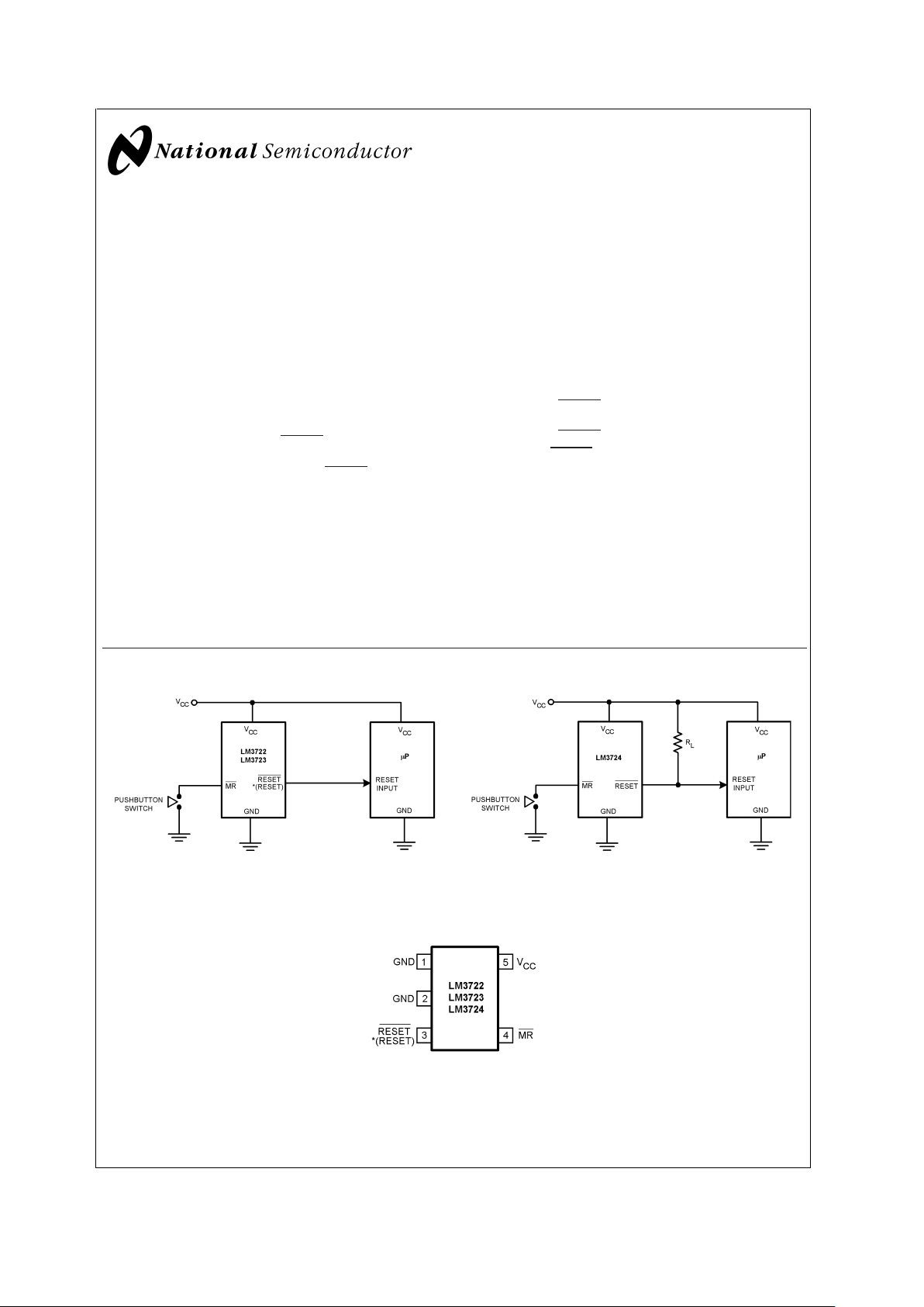
Typical Application Circuit
20014401
20014437
Connection Diagram
SOT23-5
20014402
*
( ) are for LM3723
June 2001
LM3722/LM3723/LM3724 5-Pin Microprocessor Reset Circuits
© 2001 National Semiconductor Corporation DS200144 www.national.com
Page 2
Ordering Information
Industrial Temperature Range (−40˚C to +85˚C):
Reset
Threshold (V)
LM3722 Supplied as
1000 units, tape & reel
LM3722 Supplied as
3000 units, tape & reel
Package
Top Mark
Package
Type
NSC Package
4.63 LM3722IM5-4.63 LM3722IM5X-4.63 R43B
SOT23-5 MF05A3.08 LM3722IM5-3.08 LM3722IM5X-3.08 R41B
2.32 LM3722IM5-2.32 LM3722IM5X-2.32 R34B
Reset
Threshold (V)
LM3723 Supplied as
1000 units, tape & reel
LM3723 Supplied as
3000 units, tape & reel
Package
Top Mark
Package
Type
NSC Package
4.63 LM3723IM5-4.63 LM3723IM5X-4.63 R13B
SOT23-5 MF05A3.08 LM3723IM5-3.08 LM3723IM5X-3.08 R11B
2.32 LM3723IM5-2.32 LM3723IM5X-2.32 R46B
Reset
Threshold (V)
LM3724 Supplied as
1000 units, tape & reel
LM3724 Supplied as
3000 units, tape & reel
Package
Top Mark
Package
Type
NSC Package
4.63 LM3724IM5-4.63 LM3724IM5X-4.63 R55B
SOT23-5 MF05A3.08 LM3724IM5-3.08 LM3724IM5X-3.08 R53B
2.32 LM3724IM5-2.32 LM3724IM5X-2.32 R50B
Extended Temperature Range (−40˚C to +125˚C):
Reset
Threshold (V)
LM3722 Supplied as
1000 units, tape & reel
LM3722 Supplied as
3000 units, tape & reel
Package
Top Mark
Package
Type
NSC Package
4.63 LM3722EM5-4.63 LM3722EM5X-4.63 R56B
SOT23-5 MF05A3.08 LM3722EM5-3.08 LM3722EM5X-3.08 R57B
2.32 LM3722EM5-2.32 LM3722EM5X-2.32 R58B
Reset
Threshold (V)
LM3723 Supplied as
1000 units, tape & reel
LM3723 Supplied as
3000 units, tape & reel
Package
Top Mark
Package
Type
NSC Package
4.63 LM3723EM5-4.63 LM3723EM5X-4.63 R59B
SOT23-5 MF05A3.08 LM3723EM5-3.08 LM3723EM5X-3.08 R60
2.32 LM3723EM5-2.32 LM3723EM5X-2.32 R61B
Reset
Threshold (V)
LM3724 Supplied as
1000 units, tape & reel
LM3724 Supplied as
3000 units, tape & reel
Package
Top Mark
Package
Type
NSC Package
4.63 LM3724EM5-4.63 LM3724EM5X-4.63 R62B
SOT23-5 MF05A3.08 LM3724EM5-3.08 LM3724EM5X-3.08 R63B
2.32 LM3724EM5-2.32 LM3724EM5X-2.32 R64B
Custom voltages and improved accuracies are available, subject to minimum orders. Contact your local National Semiconductor Sales Office for information.
LM3722/LM3723/LM3724
www.national.com 2
Page 3
Pin Description
PIN NAME FUNCTION
1 GND Ground reference
2 GND Ground reference, device substrate, connect to ground.
3
RESET
LM3722/LM3724
Active-low output. RESET remains low while V
CC
is below the reset threshold
voltage, and for 190 ms after VCCrises above the reset threshold voltage.
RESET
LM3723
Active-high output. RESET remains high while V
CC
is below the reset threshold, and
for 190 ms after V
CC
rises above the reset threshold.
4MR
Active-low input. Reset is asserted whenever this pin is pulled low and remains
asserted for 190 ms after the MR pin goes high. May be left open.
5VCCSupply Voltage (+5V, +3.3V, or +2.5V, nominal)
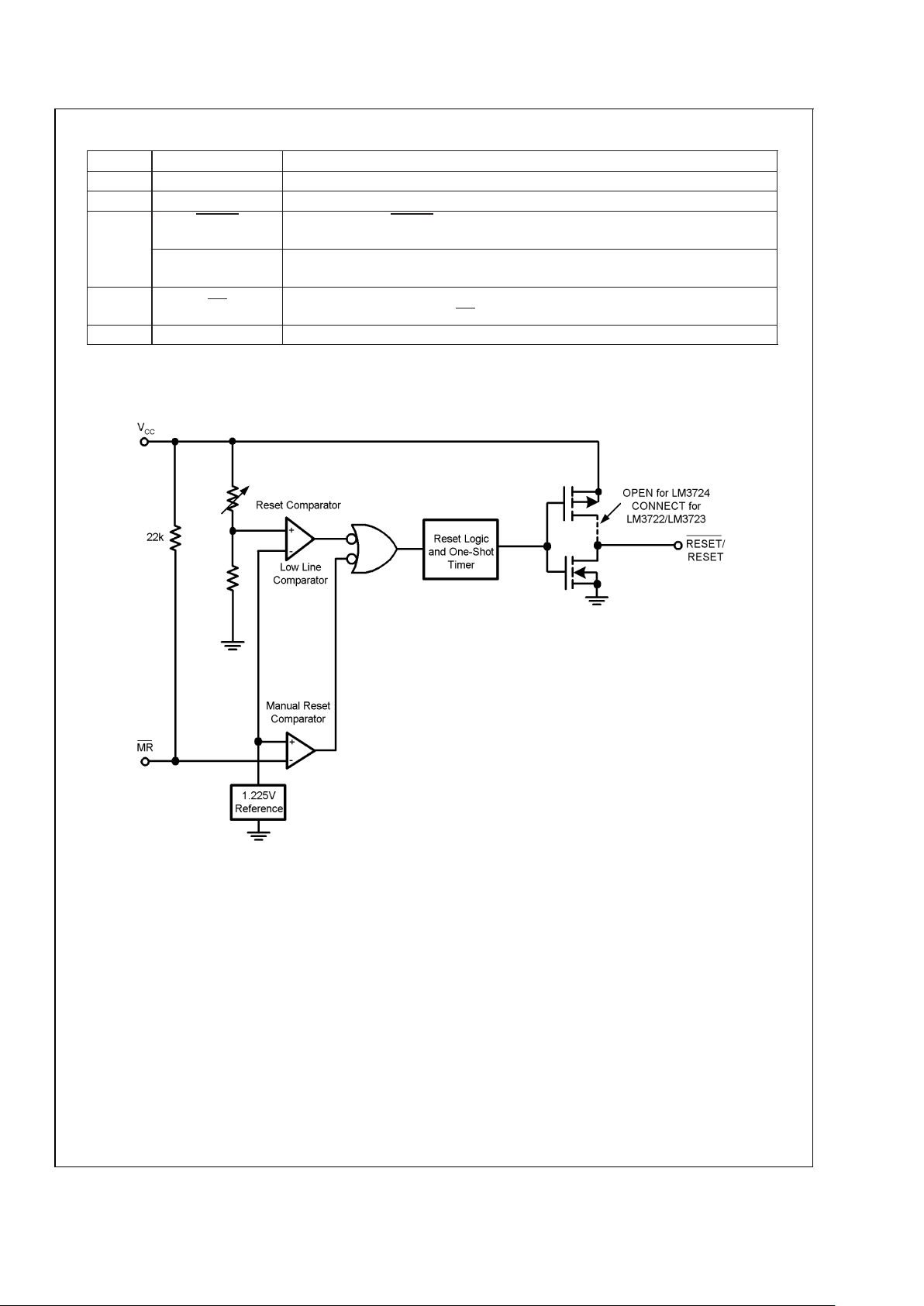
Block Diagram
LM3722/LM3723/LM3724 Block Diagram
20014435
LM3722/LM3723/LM3724
www.national.com3
Page 4
Absolute Maximum Ratings (Note 1)
If Military/Aerospace specified devices are required,
please contact the National Semiconductor Sales Office/
Distributors for availability and specifications.
V
CC
,MR −0.3V to 6.0V
RESET, RESET
−0.3V to (VCC+ 0.3V)
Input Current, V
CC
Pin 20mA
Output Current, RESET,
RESET Pin
20mA
ESD Rating (Note 2) 2kV
Continuous Power Dissipation (T
A
= +70˚C)
SOT-23 (Note 3) 320mW
Operating Temperature Range
Industrial: −40˚C to +85˚C
Extended: −40˚C to +125˚C
Maximum Junction Temperature 125˚C
Storage Temperature Range −65˚C to +160˚C
Lead Temperature
(soldering, 10sec) +300˚C
Electrical Characteristics
Typical values are at TA= +25˚C. Limits with standard typeface are for TA= +25˚C, and limits in boldface type apply for the
operating temperature range (−40˚C to +85˚C) for LM372_IM5X, and (−40˚C to +125˚C) for LM372_EM5X, unless otherwise
noted. (Note 4)
Symbol Parameter Conditions Min Typ Max Units
V
CC
VCCRange 1.0 5.5 V
I
CC
Supply Current
(I
LOAD
= 0A)
LM372 _ -4.63 V
CC
= 5.5V 8 15 µA
LM372 _ -3.08 V
CC
= 3.6V 7 10
LM372 _ -2.32 V
CC
= 2.5V 6 10
V
TH
Reset Threshold
LM372 _ -4.63
4.54
4.50
4.63 4.72
4.75
VLM372 _ -3.08
3.03
3.00
3.08 3.14
3.15
LM372 _ -2.32
2.27
2.25
2.32 2.37
2.40
V
TH
Tempco
Reset Threshold
Temperature Coefficient
30 ppm/˚C
t
RD
VCCto Reset Delay (Note 5) VCC=VTHto (VTH− 100mV) 20 µs
t
RP
Reset Active Timeout Period 100 190 560 ms
t
MR
MR Minimum Pulse Width 10 µs
t
MD
MR to Reset Propagation
Delay
2µs
MR Glitch Immunity (Note 6)
100 ns
V
IH
MR Input Threshold
V
CC
>
V
TH(MAX)
, LM372_ -4.63
2.3
V
V
IL
0.8
V
IH
V
CC
>
V
TH(MAX)
, LM372_ -3.08, LM372_
-2.32
0.7 V
CC
V
IL
0.25 V
CC
MR Pull-Up Resistance 22 kΩ
V
OL
RESET Output Voltage Low
(LM3722)
V
CC=VTH
min, I
SINK
= 1.2mA,
(LM3722-2.32/3.08)
0.3
VV
CC=VTH
min, I
SINK
= 3.2mA,
(LM3722-4.63)
0.4
V
CC
>
1V, I
SINK
= 50µA 0.3
V
OH
RESET Output Voltage High
(LM3722)
V
CC
>
VTHmax, I
SOURCE
= 500µA,
(LM3722-2.32/3.08)
0.8V
CC
V
V
CC
>
VTHmax, I
SOURCE
= 800µA,
(LM3722-4.63)
VCC−1.5
V
OL
RESET Output Voltage Low
(LM3723)
V
CC=VTH
max, I
SINK
= 1.2mA
(LM3723 -2.32/3.08)
0.3
V
V
CC=VTH
max, I
SINK
= 3.2mA
(LM3723 -4.63)
0.4
LM3722/LM3723/LM3724
www.national.com 4
Page 5

Electrical Characteristics (Continued)
Typical values are at TA= +25˚C. Limits with standard typeface are for TA= +25˚C, and limits in boldface type apply for the
operating temperature range (−40˚C to +85˚C) for LM372_IM5X, and (−40˚C to +125˚C) for LM372_EM5X, unless otherwise
noted. (Note 4)
Symbol Parameter Conditions Min Typ Max Units
V
OH
RESET Output Voltage High
(LM3723)
1.8V
<
V
CC
<
VTHmin, I
SOURCE
= 150µA
0.8V
CC
V
V
OL
RESET Output Voltage Low
(LM3724)
V
CC=VTH
min, I
SINK
= 1.2 mA
(LM3724 -2.32/3.08)
0.3 V
V
CC=VTH
min, I
SINK
= 3.2 mA
(LM3724 -4.63)
0.4
V
CC
>
1V, I
SINK
= 50µA 0.3
I
IN
RESET Output Leakage
Current (LM3724)
V
CC
>
VTH, RESET = 5.5V
0.5 µA
Note 1: Absolute Maximum Ratings are limits beyond which damage to the device may occur. Operating Ratings are conditions under which the device operates
correctly. Operating ratings do not imply guaranteed performance limits. For guaranteed performance limits and associated test conditions, see the Electrical
Characteristics.
Note 2: The human body model is a 100pF capacitor discharged through a 1.5kΩ resistor into each pin.
Note 3: At elevated temperatures, devices must be derated based on package thermal resistance. The device in the SOT23-5 package must be derated at
4.5mW/˚C at ambient temperatures above 70˚C. The device has internal thermal protection.
Note 4: Production testing done at T
A
= +25˚C. Limits over the operating temperature range are guaranteed through correlation using Statistical Quality Control
(SQC) methods.
Note 5: RESET Output for LM3722 and LM3724, RESET output for LM3723.
Note 6: Glitches of 100 ns or less typically will not generate a reset pulse.
LM3722/LM3723/LM3724
www.national.com5
Page 6

Typical Performance Characteristics
Supply Current vs V
CC
Supply Current vs Temperature
20014403 20014407
Reset Timeout vs V
CC
Reset Timeout vs Temperature
20014404
20014408
Normalized VTHvs Temperature LM3724 VOLvs Current
20014416 20014405
LM3722/LM3723/LM3724
www.national.com 6
Page 7

Typical Performance Characteristics (Continued)
LM3724 Low V
CC
Characteristics
20014406
LM3722/LM3723/LM3724
www.national.com7
Page 8

Timing Diagram
20014412
Circuit Information
Reset Output
The reset input of a µP initializes the device into a known
state. The LM3722/LM3723/LM3724 microprocessor voltage
monitoring circuits assert a forced reset output to prevent
code execution errors during power-up, power-down, and
brownout conditions.
RESET is guaranteed valid for V
CC
≥ 1V.Once VCCexceeds
the reset threshold, an internal timer maintains the output for
the reset timeout period. After this interval, reset goes high
and the microprocessor initializes itself into a known state.
The LM3722 and LM3724 offer an active-low RESET; the
LM3723 offers an active-high RESET.
As V
CC
drops below the reset threshold (such as during a
brownout), the reset activates (see the
Negative-Going V
CC
Transients
section). When VCCagain rises above the reset
threshold, the internal timer starts. Reset holds until V
CC
exceeds the reset threshold for longer than the reset timeout
period. After this time, reset releases.
Additionally, the Manual Reset input (MR) will initiate a
forced reset. See the
Manual Reset Input
section.
The LM3722/LM3723/LM3724 reset outputs ignore short duration glitches on V
CC
and MR. See the
Applications Infor-
mation
section for details.
Reset Threshold
The LM3722/LM3723/LM3724 are available with reset voltages of 4.63V, 3.08V, and 2.32V which are suitable for
monitoring 5.0V, 3.3V, and 2.5V supplies respectively. Other
reset thresholds in the 2.20V to 5.0V range, in 10 mV steps,
are available; contact National Semiconductor for details.
Manual Reset Input (MR)
Many µP-based products require a manual reset capability,
allowing the operator to initiate a reset. The MR input is fully
debounced and provides an internal22 kΩ pull-up. When the
MR input is pulled below V
IL
(0.25VCC) for more than 100 ns,
reset is asserted after a typical delay of 2 µs. Reset remains
active as long as MR is held low,andreleases after MR rises
above VIHand the reset timeout period expires. Use MR with
digital logic to assert reset or to daisy chain supervisory
circuits.
Applications Information
Benefits of Precision Reset Thresholds
A microprocessor supply supervisor must provide a reset
output within a predictable range of the supply voltage. A
common threshold range is between 5% and 10% below the
nominal supply voltage.The 4.63V,3.08V and 2.32V options
of the LM3722/LM3723/LM3724 usehighly accurate circuitry
to ensure that the reset threshold occurs only within this
range (for 5.0V, 3.3V and 2.5V supplies).
Table 1
shows how
the standard reset thresholds apply to 5.0V, 3.3V, and 2.5V
nominal supply voltages.
LM3722/LM3723/LM3724
www.national.com 8
Page 9

Applications Information (Continued)
TABLE 1. Monitored Tolerance Table
Reset
Threshold
Supply Voltage
2.5V 3.3V 5.0V
4.63
±
% 90.8-94.4%
3.08
±
% 91.8-95.2%
2.32
±
% 90.8-94.8%
Ensuring a Valid Reset Output Down to V
CC
=0V
When V
CC
falls below 1V, the LM3722 RESET output is
unable to sink the rated current. A high-impedance CMOS
logic input connected to RESET can therefore drift to undetermined voltages. Toprevent this situation, a 100kΩ resistor
should be connected from the RESET output to ground, as
shown in
Figure 1
.
A100kΩ pull-up resistor to V
CC
is also recommended for the
LM3723, if RESET is required to remain valid for V
CC
<
1V.
Open Drain Output (LM3724)
An open drain output allows easy paralleling of multiple
microprocessor reset circuits without requiring additional
logic gates. Open drain outputs also allow interfacing devices of differing logic levels or families, since the output
pull-up resistor may be connected to any supply voltage up
to 5.5V, regardless of LM3724 V
CC
.
The pull up resistor is calculated so that maximum current
flow into RESET is less than 10 mA when activated. The
resistor must be small enough so that the leakage current of
all connected devices does not create an excessive voltage
drop when the output is not activated. A resistor value of 100
kΩ will generally suffice.
Negative-Going V
CC
Transients
The LM3722/LM3723/LM3724 are relativelyimmune to short
negative-going transients or glitches on V
CC
.
Figure 2
shows
the maximum pulse width a negative-going V
CC
transient
can have without causing a reset pulse. In general, as the
magnitude of the transient increases, going further below the
threshold, the maximum allowable pulse width decreases.
Typically, a V
CC
transient that goes 125 mV below the reset
threshold and lasts 40 µs or less will not cause a reset pulse.
A 0.1 µF bypass capacitor mounted as close as possible to
the V
CC
pin will provide additional transient rejection.
Interfacing to µPs with Bidirectional Reset Pins
Microprocessors with bidirectional reset pins, such as the
Motorola 68HC11 series, can be connected to the LM3722
RESET output. To ensure a correct output on the LM3722
even when the microprocessor reset pin is in the opposite
state, connect a 4.7kΩ resistor between the LM3722 RESET
output and the µP reset pin, as shown in
Figure 3
. Buffer the
LM3722 RESET output to other system components.
20014410
FIGURE 1. Circuit for RESET Valid from VCC=0V
20014414
FIGURE 2. Maximum Transient Duration without
Causing a Reset Pulse vs. Reset Comparator
Overdrive
LM3722/LM3723/LM3724
www.national.com9
Page 10

Typical Application Circuits
20014411
FIGURE 3. Interfacing to Microprocessors with Bidirectional Reset I/O
20014422
FIGURE 4. Regulator/Switch with Long-Term Overvoltage Lockout Prevents Overdissipation in Linear Regulator
LM3722/LM3723/LM3724
www.national.com 10
Page 11

Typical Application Circuits (Continued)
20014431
FIGURE 5. LM3722 Switch Debouncer
20014424
FIGURE 6. LM3723 Power-On Delay
LM3722/LM3723/LM3724
www.national.com11
Page 12

Physical Dimensions inches (millimeters)
unless otherwise noted
5-Lead SOT23-5
For Ordering, refer to Ordering Information table
NS Package Number MF05A
LIFE SUPPORT POLICY
NATIONAL’S PRODUCTS ARE NOT AUTHORIZED FOR USE AS CRITICAL COMPONENTS IN LIFE SUPPORT
DEVICES OR SYSTEMS WITHOUT THE EXPRESS WRITTEN APPROVAL OF THE PRESIDENT AND GENERAL
COUNSEL OF NATIONAL SEMICONDUCTOR CORPORATION. As used herein:
1. Life support devices or systems are devices or
systems which, (a) are intended for surgical implant
into the body, or (b) support or sustain life, and
whose failure to perform when properly used in
accordance with instructions for use provided in the
labeling, can be reasonably expected to result in a
significant injury to the user.
2. A critical component is any component of a life
support device or system whose failure to perform
can be reasonably expected to cause the failure of
the life support device or system, or to affect its
safety or effectiveness.
National Semiconductor
Corporation
Americas
Email: support@nsc.com
National Semiconductor
Europe
Fax: +49 (0) 180-530 85 86
Email: europe.support@nsc.com
Deutsch Tel: +49 (0) 69 9508 6208
English Tel: +44 (0) 870 24 0 2171
Français Tel: +33 (0) 1 41 91 8790
National Semiconductor
Asia Pacific Customer
Response Group
Tel: 65-2544466
Fax: 65-2504466
Email: ap.support@nsc.com
National Semiconductor
Japan Ltd.
Tel: 81-3-5639-7560
Fax: 81-3-5639-7507
www.national.com
LM3722/LM3723/LM3724 5-Pin Microprocessor Reset Circuits
National does not assume any responsibility for use of any circuitry described, no circuit patent licenses are implied and National reserves the right at any time without notice to change said circuitry and specifications.
 Loading...