

Datasheet LM3704XDMMX-232, LM3704XDMMX-220, LM3704XDMM-463, LM3704XDBPX-463, LM3704XDBPX-232 Datasheet (NSC)
...Page 1
LM3704/LM3705
Microprocessor Supervisory Circuits with Power Fail
Input, Low Line Output and Manual Reset
General Description
The LM3704/LM3705 series of microprocessor supervisory
circuits provide the maximum flexibility for monitoring power
supplies and battery controlled functions in systems without
backup batteries. The LM3704/LM3705 series are available
in MSOP-10 and 9-bump micro SMD packages.
Built-in features include the following:
Reset: Reset is asserted during power-up, power-down, and
brownout conditions. RESET is guaranteed down to V
CC
of
1.0V.
Manual Reset Input: An input that asserts reset when pulled
low.
Power-Fail Input: A 1.225V threshold detector for power fail
warning, or to monitor a power supply other than V
CC
.
Low Line Output: This early power failure warning indicator
goes low when the supply voltage drops to a value which is
2% higher than the reset threshold voltage.
Features
n Standard Reset Threshold voltage: 3.08V
n Custom Reset Threshold voltages: For other voltages
between 2.2V and 5.0V in 10mV increments, contact
National Semiconductor Corp.
n No external components required
n Manual-Reset input
n RESET (LM3704) or RESET (LM3705) outputs
n Precision supply voltage monitor
n Factory programmable Reset Timeout Delay
n Separate Power Fail comparator
n Available in micro SMD package for minimum footprint
n
±
0.5% Reset threshold accuracy at room temperature
n
±
2% Reset threshold accuracy over temperature
extremes
n Reset assertion down to 1V V
CC
(RESET option only)
n 28 µA VCCsupply current
Applications
n Embedded Controllers and Processors
n Intelligent Instruments
n Automotive Systems
n Critical µP Power Monitoring
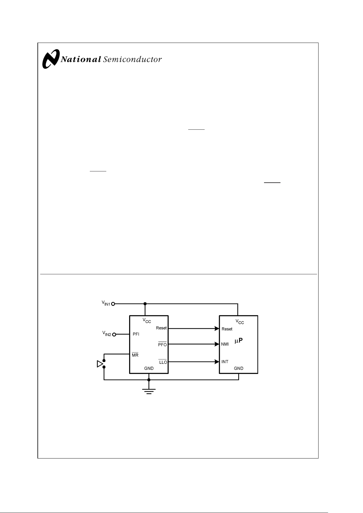
Typical Application
10136903
July 2002
LM3704/LM3705 Microprocessor Supervisory Circuits with Power Fail Input, Low Line Output and
Manual Reset
© 2002 National Semiconductor Corporation DS101369 www.national.com
Page 2
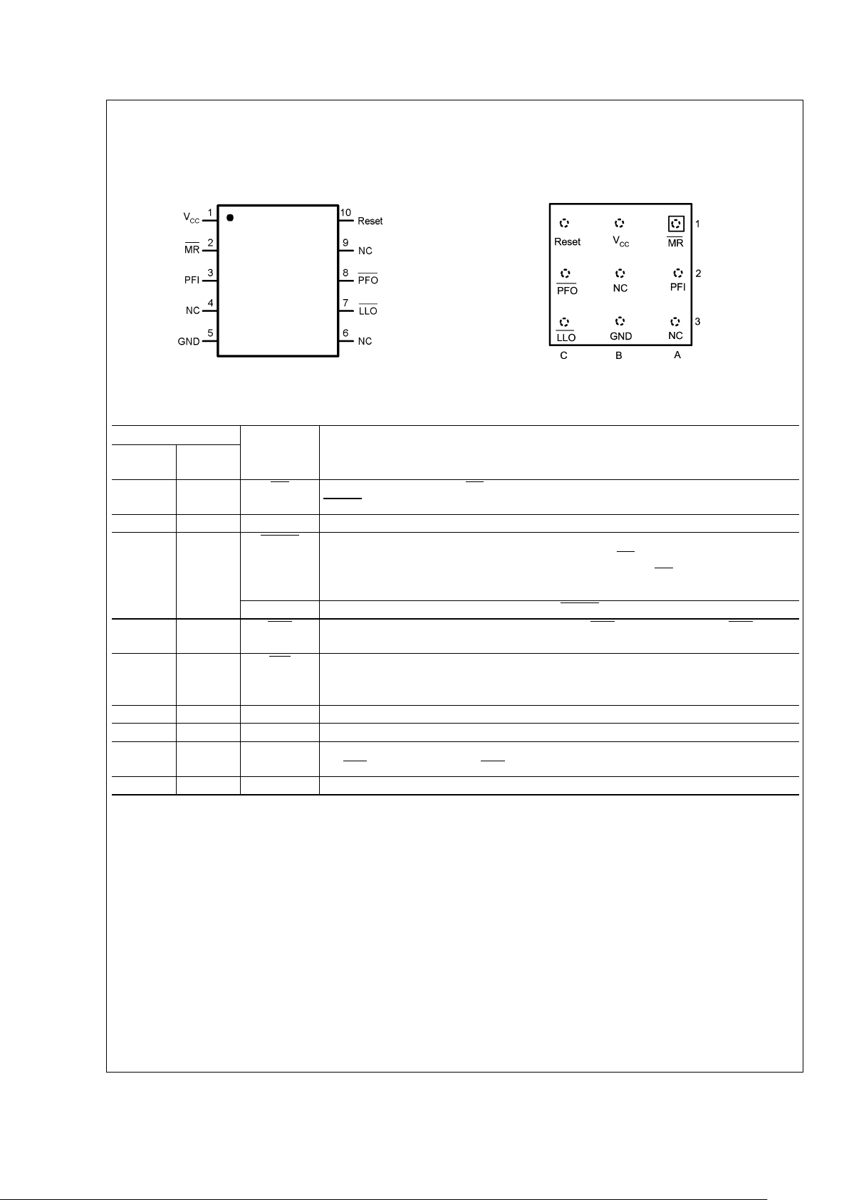
Connection Diagram
MSOP-10
Top View
(looking from the coating side)
micro SMD 9 Bump Package
BPA09
10136902
10136901
Pin Description
Pin No.
Name Function
micro
SMD
MSOP
A1 2 MR
Manual-Reset input. When MR is less than V
MRT
(Manual Reset Threshold)
RESET/RESET is engaged.
B1 1 V
CC
Power Supply input.
C1 10 RESET
Reset Logic Output. Pulses low for tRP(Reset Timeout Period) when triggered, and stays
low whenever V
CC
is below the reset threshold or when MR is below V
MRT
. It remains low
for tRPafter either VCCrises above the reset threshold, or after MR input rises above
V
MRT
(LM3704 only).
RESET Reset Logic Output. RESET is the inverse of RESET (LM3705 only).
C2 8 PFO Power-Fail Logic Output. When PFI is below V
PFT
, PFO goes low; otherwise, PFO
remains high.
C3 7 LLO
Low-Line Logic Output. Early Power-Fail warning output. Low when VCCfalls below V
LLOT
(Low-Line Output Threshold). This output can be used to generate an NMI (Non-Maskable
Interrupt) to provide an early warning of imminent power-failure.
B3 5 GND Ground reference for all signals.
A3 4, 6 NC No Connect.
A2 3 PFI Power-Fail Comparator Input. When PFI is less than V
PFT
(Power-Fail Reset Threshold),
the PFO goes low; otherwise, PFO remains high.
B2 9 NC No Connect. Test input used at factory only. Leave floating.
LM3704/LM3705
www.national.com 2
Page 3
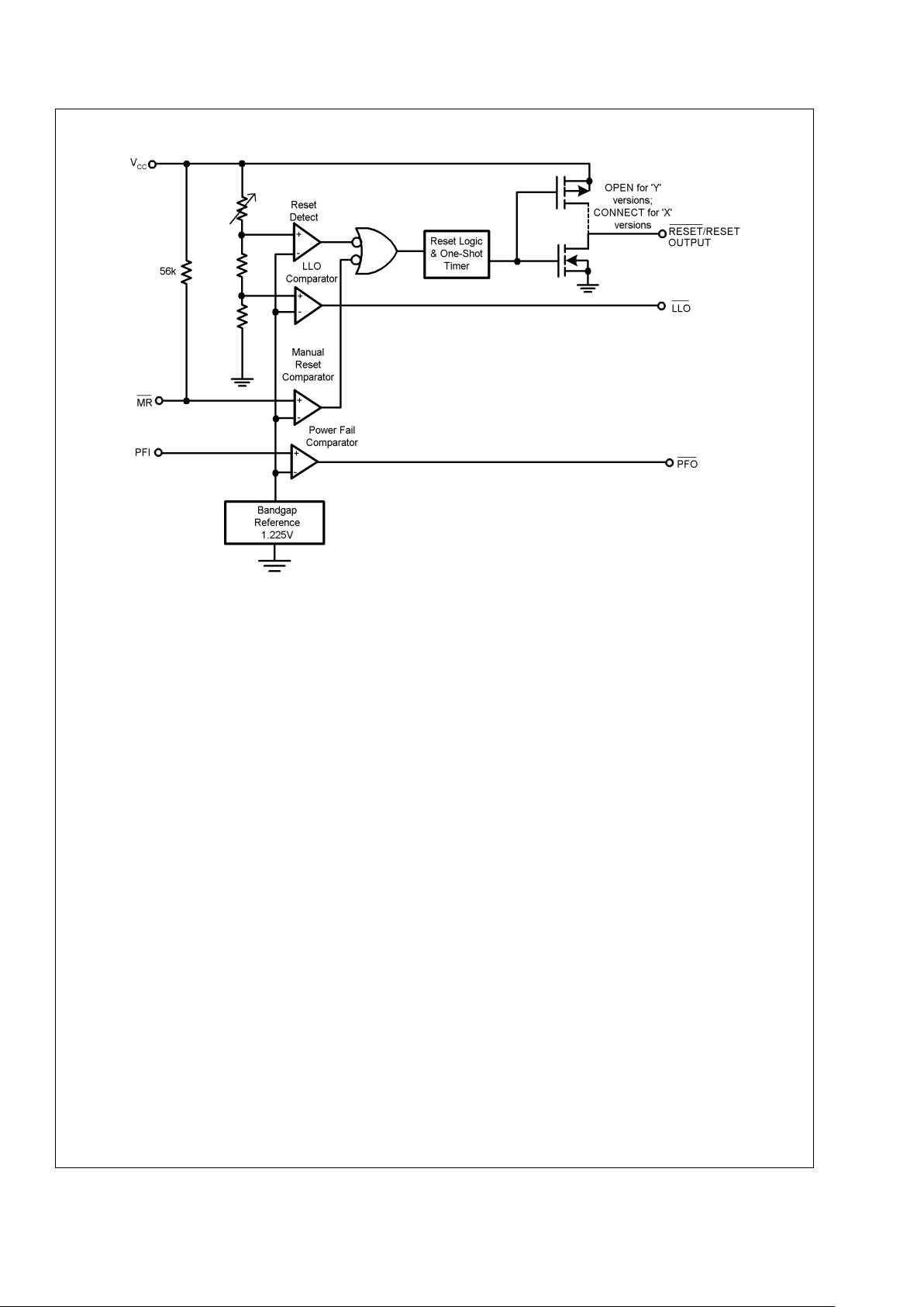
Block Diagram
10136926
LM3704/LM3705
www.national.com3
Page 4
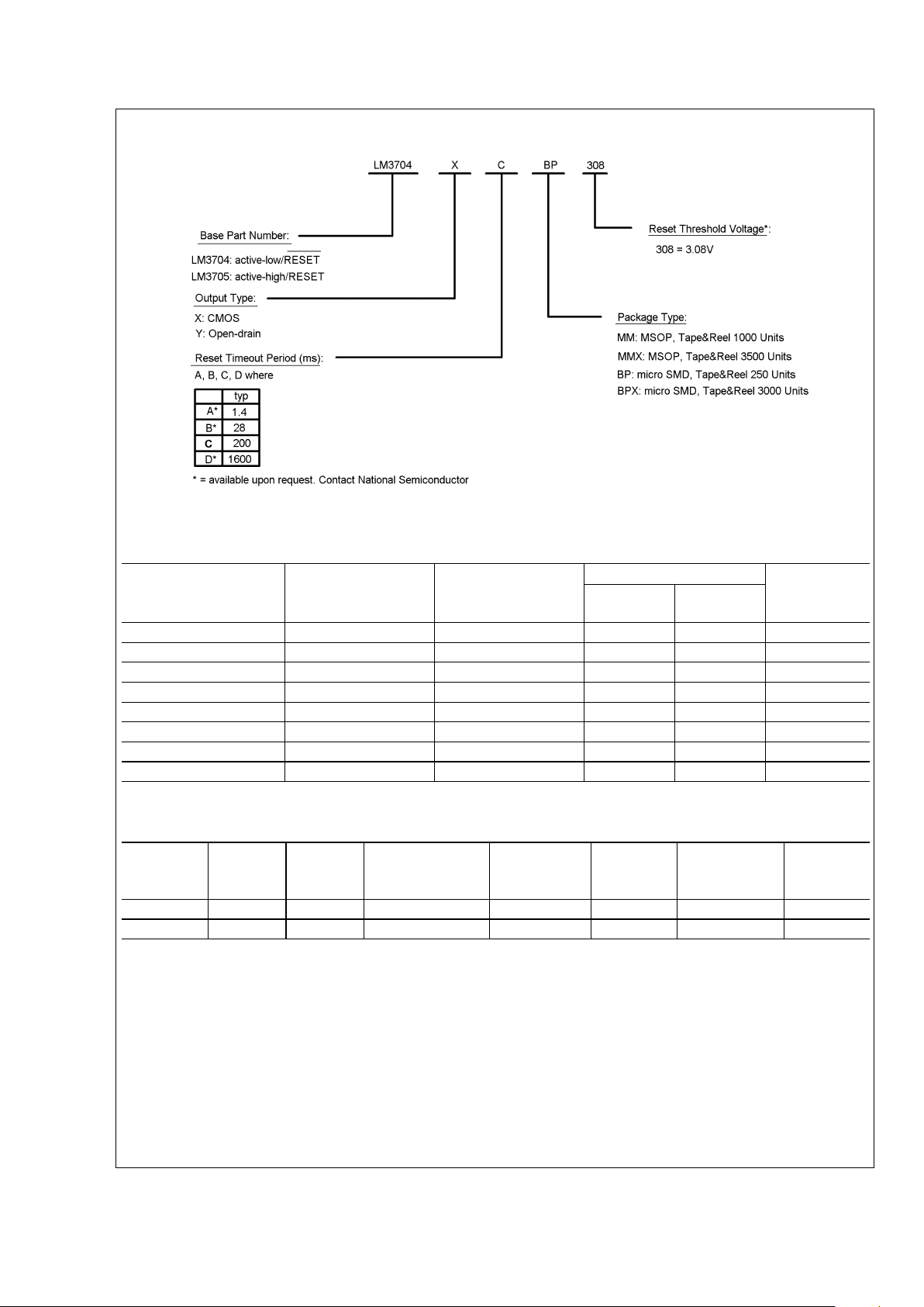
Ordering Information
10136904
*
For other voltages between 2.2V and 5.0V, please contact National Semiconductor sales office.
LM3704/LM3705
Part Number Output
Reset Timeout
Period
Package
Package
Marking
MSOP
micro
SMD
LM3704XCBP-308 totem-pole 200ms x %%I4
LM3704XCBPX-308 totem-pole 200ms x %%I4
LM3704XCMM-308 totem-pole 200ms x R35B
LM3704XCMMX-308 totem-pole 200ms x R35B
LM3705XCBP-308 totem-pole 200ms x %%I5
LM3705XCBPX-308 totem-pole 200ms x %%I5
LM3705XCMM-308 totem-pole 200ms x R36B
LM3705XCMMX-308 totem-pole 200ms x R36B
%% is the datecode and will vary with time.
Table Of Functions
Part
Number
Active
Low
Reset
Active
High
Reset
Output
(X = totem-pole)
(Y = open-drain)
Reset
Timeout
Period
Manual
Reset
Power Fail
Comparator
Low
Line
Output
LM3704 x X, Y
*
Customized x x x
LM3705 x X Customized x x x
*
= available upon request. Contact National
LM3704/LM3705
www.national.com 4
Page 5
Absolute Maximum Ratings (Note 1)
If Military/Aerospace specified devices are required,
please contact the National Semiconductor Sales Office/
Distributors for availability and specifications.
Supply Voltage (V
CC
) −0.3V to 6.0V
All Other Inputs −0.3V to V
CC
+ 0.3V
ESD Ratings (Note 2)
Human Body Model
Machine Model
1.5kV
150V
Power Dissipation (Note 3)
Operating Ratings (Note 1)
Temperature Range −40˚C ≤ T
J
≤ 85˚C
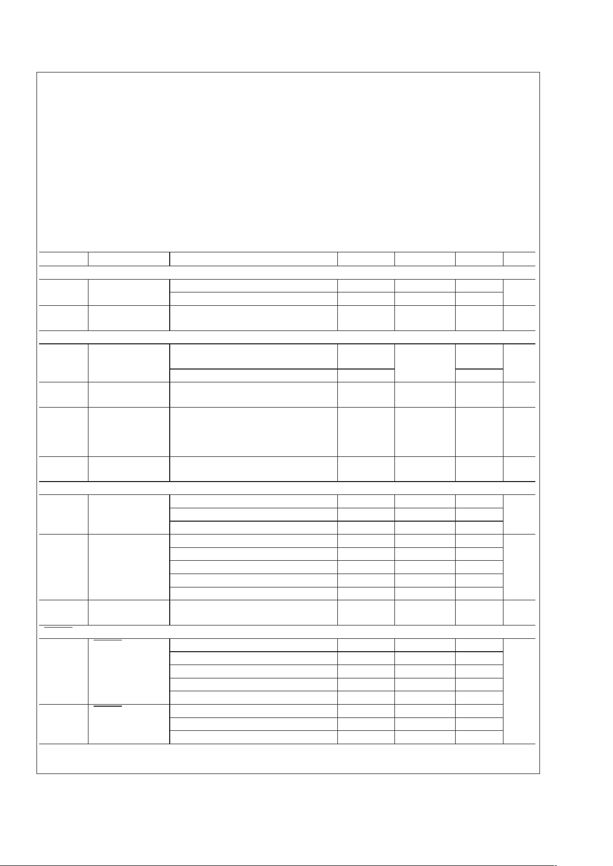
LM3704/LM3705 Series Electrical Characteristics
Limits in the standard typeface are for TJ= 25˚C and limits in boldface type apply over full operating range. Unless otherwise
specified: V
CC
= +2.2V to 5.5V.
Symbol Parameter Conditions Min Typ Max Units
POWER SUPPLY
V
CC
Operating Voltage
Range: V
CC
LM3704 1.0 5.5
V
LM3705 1.2 5.5
I
CC
VCCSupply
Current
All inputs = VCC; all outputs floating 28 50 µA
RESET THRESHOLD
V
RST
Reset Threshold VCCfalling −0.5
−2
V
RST
+0.5
+2
%
V
CC
falling: TA= 0˚C to 70˚C −1.5 +1.5
V
RSTH
Reset Threshold
Hysteresis
0.0032•V
RST
mV
t
RP
Reset Timeout
Period
Reset Timeout Period = A
Reset Timeout Period = B
Reset Timeout Period = C
Reset Timeout Period = D
1
20
140
1120
1.4
28
200
1600
2
40
280
2240
ms
t
RD
VCCto Reset
Delay
VCCfalling at 1mV/µs 20 µs
RESET (LM3705)
V
OL
RESET V
CC
>
2.25V, I
SINK
= 900µA 0.3
VV
CC
>
2.7V, I
SINK
= 1.2mA 0.3
V
CC
>
4.5V, I
SINK
= 3.2mA 0.4
V
OH
RESET V
CC
>
1.2V, I
SOURCE
= 50µA 0.8 V
CC
V
V
CC
>
1.8V, I
SOURCE
= 150µA 0.8 V
CC
V
CC
>
2.25V, I
SOURCE
= 300µA 0.8 V
CC
V
CC
>
2.7V, I
SOURCE
= 500µA 0.8 V
CC
V
CC
>
4.5V, I
SOURCE
= 800µA VCC− 1.5V
I
LKG
Output Leakage
Current
V
RESET
= 5.5V 1.0 µA
RESET (LM3704)
V
OL
RESET V
CC
>
1.0V, I
SINK
= 50µA 0.3
V
V
CC
>
1.2V, I
SINK
= 100µA 0.3
V
CC
>
2.25V, I
SINK
= 900µA 0.3
V
CC
>
2.7V, I
SINK
= 1.2mA 0.3
V
CC
>
4.5V, I
SINK
= 3.2mA 0.4
V
OH
RESET V
CC
>
2.25V, I
SOURCE
= 300µA 0.8 V
CC
V
CC
>
2.7V, I
SOURCE
= 500µA 0.8 V
CC
V
CC
>
4.5V, I
SOURCE
= 800µA VCC− 1.5V
LM3704/LM3705
www.national.com5
Page 6

LM3704/LM3705 Series Electrical Characteristics (Continued)
Limits in the standard typeface are for TJ= 25˚C and limits in boldface type apply over full operating range. Unless otherwise
specified: V
CC
= +2.2V to 5.5V.
Symbol Parameter Conditions Min Typ Max Units
PFI/MR
V
PFT
PFI Input
Threshold
1.200 1.225 1.250 V
V
MRT
MR Input
Threshold
MR, Low
0.8
V
MR, High
2.0
V
PFTH
/
V
MRTH
PFI/MR Threshold
Hysteresis
PFI/MR falling: V
CC=VRST MAX
to 5.5V 0.0032•V
RST
mV
I
PFI
Input Current (PFI
only)
−75 75 nA
R
MR
MR Pull-up
Resistance
35 56 75 kΩ
t
MD
MR to Reset
Delay
12 µS
t
MR
MR Pulse Width 25 µS
PFO, LLO
V
OL
PFO, LLO Output
Voltage
V
CC
>
2.25V, I
SINK
= 900µA 0.3
V
V
CC
>
2.7V, I
SINK
= 1.2mA 0.3
V
CC
>
4.5V, I
SINK
= 3.2mA 0.4
V
OH
V
CC
>
2.25V, I
SOURCE
= 300µA 0.8 V
CC
V
CC
>
2.7V, I
SOURCE
= 500µA 0.8 V
CC
V
CC
>
4.5V, I
SOURCE
= 800µA VCC− 1.5V
LLO OUTPUT
V
LLOT
LLO Output
Threshold
(V
LLO−VRST,VCC
falling)
1.01
•
V
RST
1.02•V
RST
1.03•V
RST
V
V
LLOTH
Low-Line
Comparator
Hysteresis
0.0032
•
V
RST
mV
t
CD
Low-Line
Comparator Delay
VCCfalling at 1mV/µs 20 µs
Note 1: Absolute Maximum Ratings indicate limits beyond which damage to the device may occur. Operating Ratings indicate conditions for which the device
is intended to be functional, but do not guarantee specific performance limits. For guaranteed specifications and test conditions, see the Electrical Characteristics.
The guaranteed specifications apply only for the test conditions listed. Some performance characteristics may degrade when the device is not operated under the
listed conditions.
Note 2: The Human Body model is a 100 pF capacitor discharged through a 1.5 kΩ resistor into each pin. The machine model is a 200pF capacitor discharged
directly into each pin.
Note 3: The maximum allowable power dissipation is a function of the maximum junction temperature, T
J
(MAX), the junction-to-ambient thermal resistance, θ
J-A
,
and the ambient temperature, T
A
. The maximum allowable power dissipation at any ambient temperture is calculated using:
Where the value of θ
J-A
for the MSOP-10 package is 195˚C/W in a typical PC board mounting and the micro SMD package is 220˚C/W.
LM3704/LM3705
www.national.com 6
Page 7

Typical Performance Characteristics
Supply Current vs Supply Voltage 3.3V Supply Current vs Temperature
10136915
10136911
Normalized Reset Threshold Voltage vs Temperature Reset Timeout Period vs V
CC
10136912
10136932
Reset Timeout Period vs Temperature
Max. Transient Duration vs Reset Comparator Overdrive
(VCC= 3.3V)
10136910
10136916
LM3704/LM3705
www.national.com7
Page 8

Typical Performance Characteristics (Continued)
Low-Line Comparator Propagation Delay vs Temperature
10136914
LM3704/LM3705
www.national.com 8
Page 9

Circuit Information
Reset Output
The Reset input of a µP initializes the device into a known
state. The LM3704/LM3705 microprocessor supervisory circuits assert a forced reset output to prevent code execution
errors during power-up, power-down, and brownout conditions.
RESET is guaranteed valid for V
CC
>
1V. Once VCCexceeds the reset threshold, an internal timer maintains the
output for the reset timeout period. After this interval, reset
goes high. The LM3704 offers an active-low RESET; The
LM3705 offers an active-high RESET.
Any time V
CC
drops below the reset threshold (such as
during a brownout), the reset activates. When V
CC
again
rises above the reset threshold, the internal timer starts.
Reset holds until V
CC
exceeds the reset threshold for longer
than the reset timeout period. After this time, reset releases.
The Manual Reset input (MR) will initiate a forced reset also.
See the Manual Reset Input section.
Reset Threshold
The LM3704/LM3705 family is available with a reset voltage
of 3.08V. Other reset thresholds in the 2.20V to 5.0V range,
in steps of 10 mV, are available; contact National Semiconductor for details.
Manual Reset Input (MR)
Many µP-based products require a manual reset capability,
allowing the operator to initiate a reset. The MR input is fully
debounced and provides an internal 56 kΩ pull-up. When the
MR input is pulled below V
MRT
(1.225V) for more than 25 µs,
reset is asserted after a typical delay of 12 µs. Reset remains
active as long as MR is held low, and releases after the reset
timeout period expires after MR rises above V
MRT
. Use MR
with digital logic to assert or to daisy chain supervisory
circuits. It may be used as another low-line comparator by
adding a buffer.
Power-Fail Comparator (PFI/PFO)
The PFI is compared to a 1.225V internal reference, V
PFT
.If
PFI is less than V
PFT
, the Power Fail Output PFO drops low.
The power-fail comparator signals a falling power supply,
and is driven typically by an external voltage divider that
senses either the unregulated supply or another system
supply voltage. The voltage divider generally is chosen so
the voltage at PFI drops below V
PFT
several milliseconds
before the main supply voltage drops below the reset threshold, providing advanced warning of a brownout.
The voltage threshold is set by R
1
and R2and is calculated
as follows:
Note this comparator is completely separate from the rest of
the circuitry, and may be employed for other functions as
needed.
Low-Line Output (LLO)
The low-line output comparator is typically used to provide a
non-maskable interrupt to a µP when V
CC
begins falling. LLO
monitors VCCand goes low when VCCfalls below V
LLOT
(typically 1.02•V
RST
) with hysteresis of 0.0032•V
RST
.
Special Precautions for the micro SMD Package
As with most integrated circuits, the LM3704 and LM3705
are sensitive to exposure from visible and infrared (IR) light
radiation. Unlike a plastic encapsulated IC, the micro SMD
package has very limited shielding from light, and some
sensitivity to light reflected from the surface of the PC board
or long wavelength IR entering the die from the side may be
experienced. This light could have an unpredictable affect on
the electrical performance of the IC. Care should be taken to
shield the device from direct exposure to bright visible or IR
light during operation.
Micro SMD Mounting
The micro SMD package requires specific mounting techniques which are detailed in National Semiconductor Application Note AN-1112. Referring to the section Surface
Mount Technology (SMT) Assembly Considerations,it
should be noted that the pad style which must be used with
the 9-pin package is the NSMD (non-solder mask defined)
type.
For best results during assembly, alignment ordinals on the
PC board may be used to facilitate placement of the micro
SMD device.
LM3704/LM3705
www.national.com9
Page 10

Timing Diagrams
10136928
FIGURE 1. LM3704 Reset Time with MR
10136929
FIGURE 2. LLO Output
10136930
FIGURE 3. PFI Comparator Timing Diagram
LM3704/LM3705
www.national.com 10
Page 11

Typical Application Circuits
10136918
FIGURE 4. Monitoring Two Critical Supplies
10136919
FIGURE 5. Monitoring Two Supplies plus Manual Reset
LM3704/LM3705
www.national.com11
Page 12

Typical Application Circuits (Continued)
10136920
FIGURE 6. Monitoring Dual Supplies plus External Fault Input
10136921
Note: MR input with its 1.225V nominal threshold, may monitor an additional supply voltage. An internal 56 kΩ pull-up resistor is
included on this input.
FIGURE 7. Microprocessor Supervisor with Early Warning Detector
LM3704/LM3705
www.national.com 12
Page 13

Typical Application Circuits (Continued)
10136924
FIGURE 8. LM3705 Power-On Delay
LM3704/LM3705
www.national.com13
Page 14

Typical Application Circuits (Continued)
10136923
FIGURE 9. LM3705 Power-On Delay with Overvoltage Protection
LM3704/LM3705
www.national.com 14
Page 15

Typical Application Circuits (Continued)
10136922
FIGURE 10. Regulator/Switch with Long-Term Overvoltage Lockout Prevents Overdissipation in Linear Regulator
10136931
FIGURE 11. Switch Debouncer
LM3704/LM3705
www.national.com15
Page 16

Physical Dimensions inches (millimeters)
unless otherwise noted
10 Lead MSOP Package
NS Package Number MUB10A
LM3704/LM3705
www.national.com 16
Page 17

Physical Dimensions inches (millimeters) unless otherwise noted (Continued)
NOTES: UNLESS OTHERWISE SPECIFIED
1. EPOXY COATING
2. 63Sn/37Pb EUTECTIC BUMP
3. RECOMMEND NON-SOLDER MASK DEFINED LANDING PAD.
4. PIN 1 IS ESTABLISHED BY LOWER LEFT CORNER WITH RESPECT TO TEXT ORIENTATION. REMAINING PINS ARE NUMBERED COUNTER
CLOCKWISE.
5. XXX IN DRAWING NUMBER REPRESENTS PACKAGE SIZE VARIATION WHERE X1 IS PACKAGE WIDTH, X2 IS PACKAGE LENGTH AND X3 IS
PACKAGE HEIGHT.
6.NO JEDEC REGISTRATION AS OF AUG.1999.
9 bump micro SMD Package
NS Package Number BPA09FFB
The dimensions of X1, X2 and X3 are given below
X1 = 1.412mm
X2 = 1.412mm
X3 = 0.850mm
LIFE SUPPORT POLICY
NATIONAL’S PRODUCTS ARE NOT AUTHORIZED FOR USE AS CRITICAL COMPONENTS IN LIFE SUPPORT
DEVICES OR SYSTEMS WITHOUT THE EXPRESS WRITTEN APPROVAL OF THE PRESIDENT AND GENERAL
COUNSEL OF NATIONAL SEMICONDUCTOR CORPORATION. As used herein:
1. Life support devices or systems are devices or
systems which, (a) are intended for surgical implant
into the body, or (b) support or sustain life, and
whose failure to perform when properly used in
accordance with instructions for use provided in the
labeling, can be reasonably expected to result in a
significant injury to the user.
2. A critical component is any component of a life
support device or system whose failure to perform
can be reasonably expected to cause the failure of
the life support device or system, or to affect its
safety or effectiveness.
National Semiconductor
Corporation
Americas
Email: support@nsc.com
National Semiconductor
Europe
Fax: +49 (0) 180-530 85 86
Email: europe.support@nsc.com
Deutsch Tel: +49 (0) 69 9508 6208
English Tel: +44 (0) 870 24 0 2171
Français Tel: +33 (0) 1 41 91 8790
National Semiconductor
Asia Pacific Customer
Response Group
Tel: 65-2544466
Fax: 65-2504466
Email: ap.support@nsc.com
National Semiconductor
Japan Ltd.
Tel: 81-3-5639-7560
Fax: 81-3-5639-7507
www.national.com
LM3704/LM3705 Microprocessor Supervisory Circuits with Power Fail Input, Low Line Output and
Manual Reset
National does not assume any responsibility for use of any circuitry described, no circuit patent licenses are implied and National reserves the right at any time without notice to change said circuitry and specifications.
 Loading...