

Page 1
LM3677 Evaluation Board
National Semiconductor
Application Note 1595
Jingdong Chen
March 2007
Introduction
The LM3677 evaluation board is a working demonstration of
a step down DC-DC converter. This application note contains
information about the evaluation board. For further information on buck converter topology, device electrical characteristics, and component selection please refer to the datasheet.
General Description
The LM3677 converts high input voltages to lower output voltages with high efficiency through an inductor based switching
topology. Automatic intelligent switching between PWM lownoise and PFM low-current mode offers improved system
control. LM3677 is available in both fixed output voltage options and adjustable voltage options range from 1.2V to 3.3V
in a micro SMD-5 package. The fixed output voltage options
available in a SMD-5 package are 1.2V, 1.3V, 1.5V, 1.6V,
1.8V, 2.5V, 2.8V, and 3.3V.
Operating Conditions
•
Recommended input voltage range:
VIN = 2.7V to 4.5V for 1.1V ≤ V
OUT
< 1.5V
VIN = 2.7V to 5.5V for 1.5V ≤ V
OUT
< 1.8V
VIN = (V
OUT
+ V
DROPOUT
) to 5.5V for 1.8V ≤ V
OUT
≤ 3.3V
where V
DROPOUT
= I
LOAD
* (R
DSON, PFET
+ R
INDUCTOR
)
•
Recommended load current: 0 mA ≤ I
OUT
≤ 600 mA
•
Ambient temperature (TA) range: -30C to +85C
•
Junction temperature (TJ) range: -30C to +125C
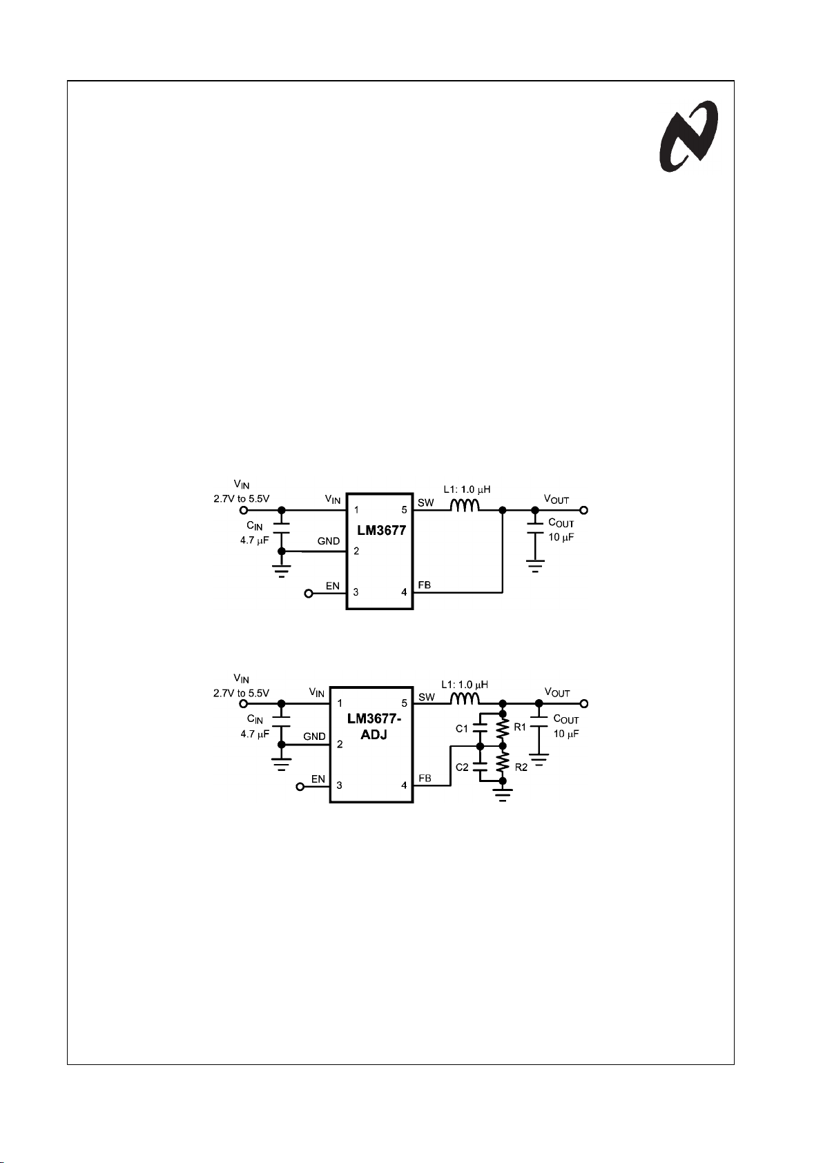
Typical Application
30012025
FIGURE 1. Fixed Output Voltage--Typical Application Circuit
30012026
FIGURE 2. Adjustable Output Voltage—Typical Application Circuit
© 2007 National Semiconductor Corporation 300120 www.national.com
LM3677 Evaluation Board AN-1595
Page 2
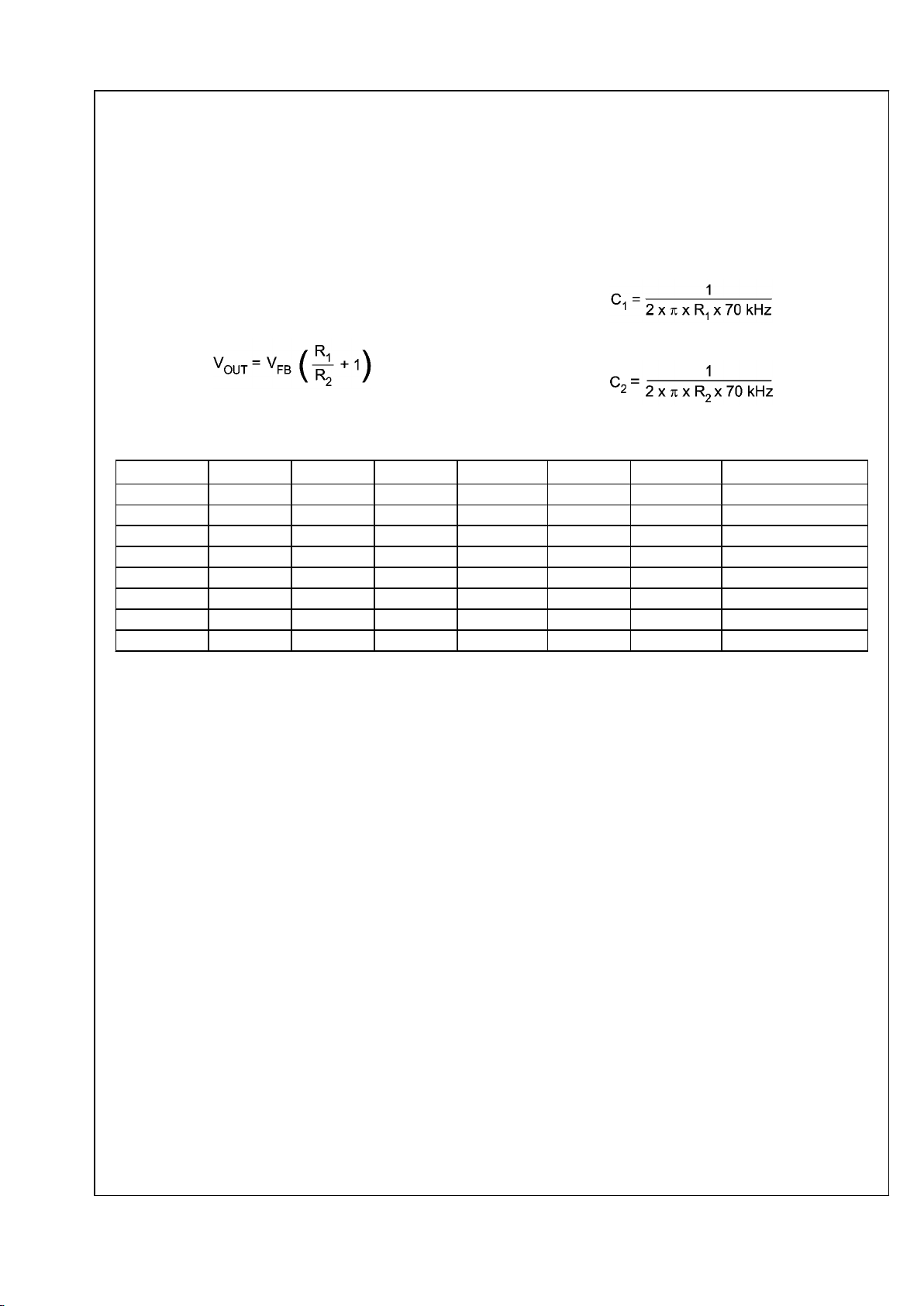
Output Voltage Selection for
LM3677TL-ADJ
The output voltage of the adjustable parts can be programmed through the resistor network connected from V
OUT
to FB to GND. The resistor from FB to GND (R2) should be
200kΩ to keep the current drawn throught this network well
below 16µA quiescent current level (PFM mode) but large
enough that it is not susceptible to noise. If R2 is 200kΩ, and
given the VFB is 0.5V, then the current through the resistor
feedback network will be 2.5µA. The ouput voltage of the adjustable parts ranges from 1.2V to 3.3V. The output voltage
formula is:
V
OUT
: output voltage (V)
VFB: feedback voltage (0.5V typical)
R1: feedback resistor from V
OUT
to FB(Ω )
R2: feedback resistor from FB to GND (Ω)
For the fixed output voltage parts the feedback resistors are
internal and R1 is 0Ω.
The bypass capacitors C1and C2 (labeled C3 and C4 on Eval-
uation Board) in parallel with the feedback resistors are chosen for increased stability. Below are the formulas for C1and
C2.
Table1. LM3677-ADJ Configurations for Various V
out
(Circuit of Figure 2)
V
OUT
(V)
R1(kΩ ) R2(kΩ )
C1(pF) C2(pF) L (µH) CIN (µF) C
OUT
(µF)
1.2 280 200 8.2 none 1.0 4.7 10
1.3 320 200 8.2 none 1.0 4.7 10
1.5 357 178 6.8 none 1.0 4.7 10
1.6 442 200 5.6 none 1.0 4.7 10
1.8 464 178 5.6 none 1.0 4.7 10
2.5 402 100 6.0 none 1.0 4.7 10
2.8 464 100 5.6 24 1.0 4.7 10
3.3 562 100 5.6 24 1.0 4.7 10
www.national.com 2
AN-1595
Page 3

Connection Diagram and Package Mark Information
30012012
FIGURE 3. 5-bump micro SMD Package
Table2. Pin Descriptions (5-bump micro SMD)
Pin# Name Description
A1 V
IN
Power supply input. Connect to the input filter capacitor
A3 GND Ground pin
C1 EN Enable pin. The device is in shutdown mode when voltage to this pin is <0.4V and enabled when
>1.0V. Do not leave this pin floating.
C3 FB Feedback analog input. Connect to the output filter capacitor for fixed voltage versions. For
adjustable version external resistor dividers are required (Figure 2). The internal resistor dividers
are disabled for the adjustable version.
B2 SW Switching node connection to the internal PFET switch and NFET synchronous rectifier. Connect
to an inductor with a saturation current rating that exceeds the 750 mA max. Switch Peak Current
Limit Specification.
3 www.national.com
AN-1595
Page 4

Evaluation Board Layout
30012024
FIGURE 4. Top Layer (5-bump micro SMD)
30012023
FIGURE 5. Bottom Layer (5-bump micro SMD)
www.national.com 4
AN-1595
Page 5

BOM For Common Configurations
Manufacture Manufacture # Description
LM3677TL - 1.8V FIXED
C1 (input C) TDK C1608X5R0J475K 4.7 µF, 6.3V, 0603, 10%
C2 (output C) TDK C1608X5R0J106K 10 µF, 6.3V, 0603, 10%
L1 (inductor) FDK MIPSA2520D 1R0 1.0 µH chip inductor
R1 (V
OUT
to VFB ) Vishay CRCW06030R00F
0Ω, 0603, 1%
R2 (VFB to GND) None
C3 (V
OUT
to VFB) None
C4 (VFB to GND) None
VIN banana jack - red Johnson
Components
108-0902-001 connector, insulated banana jack (red)
V
OUT
banana jack - yellow Johnson
Components
108-0907-001 connector, insulated banana jack (yellow)
GND banana jack - black Johnson
Components
108-0903-001 connector, insulated banana jack (black)
5 www.national.com
AN-1595
Page 6

Notes
AN-1595 LM3677 Evaluation Board
THE CONTENTS OF THIS DOCUMENT ARE PROVIDED IN CONNECTION WITH NATIONAL SEMICONDUCTOR CORPORATION
(“NATIONAL”) PRODUCTS. NATIONAL MAKES NO REPRESENTATIONS OR WARRANTIES WITH RESPECT TO THE ACCURACY
OR COMPLETENESS OF THE CONTENTS OF THIS PUBLICATION AND RESERVES THE RIGHT TO MAKE CHANGES TO
SPECIFICATIONS AND PRODUCT DESCRIPTIONS AT ANY TIME WITHOUT NOTICE. NO LICENSE, WHETHER EXPRESS,
IMPLIED, ARISING BY ESTOPPEL OR OTHERWISE, TO ANY INTELLECTUAL PROPERTY RIGHTS IS GRANTED BY THIS
DOCUMENT.
TESTING AND OTHER QUALITY CONTROLS ARE USED TO THE EXTENT NATIONAL DEEMS NECESSARY TO SUPPORT
NATIONAL’S PRODUCT WARRANTY. EXCEPT WHERE MANDATED BY GOVERNMENT REQUIREMENTS, TESTING OF ALL
PARAMETERS OF EACH PRODUCT IS NOT NECESSARILY PERFORMED. NATIONAL ASSUMES NO LIABILITY FOR
APPLICATIONS ASSISTANCE OR BUYER PRODUCT DESIGN. BUYERS ARE RESPONSIBLE FOR THEIR PRODUCTS AND
APPLICATIONS USING NATIONAL COMPONENTS. PRIOR TO USING OR DISTRIBUTING ANY PRODUCTS THAT INCLUDE
NATIONAL COMPONENTS, BUYERS SHOULD PROVIDE ADEQUATE DESIGN, TESTING AND OPERATING SAFEGUARDS.
EXCEPT AS PROVIDED IN NATIONAL’S TERMS AND CONDITIONS OF SALE FOR SUCH PRODUCTS, NATIONAL ASSUMES NO
LIABILITY WHATSOEVER, AND NATIONAL DISCLAIMS ANY EXPRESS OR IMPLIED WARRANTY RELATING TO THE SALE
AND/OR USE OF NATIONAL PRODUCTS INCLUDING LIABILITY OR WARRANTIES RELATING TO FITNESS FOR A PARTICULAR
PURPOSE, MERCHANTABILITY, OR INFRINGEMENT OF ANY PATENT, COPYRIGHT OR OTHER INTELLECTUAL PROPERTY
RIGHT.
LIFE SUPPORT POLICY
NATIONAL’S PRODUCTS ARE NOT AUTHORIZED FOR USE AS CRITICAL COMPONENTS IN LIFE SUPPORT DEVICES OR
SYSTEMS WITHOUT THE EXPRESS PRIOR WRITTEN APPROVAL OF THE CHIEF EXECUTIVE OFFICER AND GENERAL
COUNSEL OF NATIONAL SEMICONDUCTOR CORPORATION. As used herein:
Life support devices or systems are devices which (a) are intended for surgical implant into the body, or (b) support or sustain life and
whose failure to perform when properly used in accordance with instructions for use provided in the labeling can be reasonably expected
to result in a significant injury to the user. A critical component is any component in a life support device or system whose failure to perform
can be reasonably expected to cause the failure of the life support device or system or to affect its safety or effectiveness.
National Semiconductor and the National Semiconductor logo are registered trademarks of National Semiconductor Corporation. All other
brand or product names may be trademarks or registered trademarks of their respective holders.
Copyright© 2007 National Semiconductor Corporation
For the most current product information visit us at www.national.com
National Semiconductor
Americas Customer
Support Center
Email:
new.feedback@nsc.com
Tel: 1-800-272-9959
National Semiconductor Europe
Customer Support Center
Fax: +49 (0) 180-530-85-86
Email: europe.support@nsc.com
Deutsch Tel: +49 (0) 69 9508 6208
English Tel: +49 (0) 870 24 0 2171
Français Tel: +33 (0) 1 41 91 8790
National Semiconductor Asia
Pacific Customer Support Center
Email: ap.support@nsc.com
National Semiconductor Japan
Customer Support Center
Fax: 81-3-5639-7507
Email: jpn.feedback@nsc.com
Tel: 81-3-5639-7560
www.national.com
 Loading...