

Page 1
March 2007
LM3677
3MHz, 600mA Miniature Step-Down DC-DC Converter for
Ultra Low Voltage Circuits
General Description
The LM3677 step-down DC-DC converter is optimized for
powering ultra-low voltage circuits from a single Li-Ion cell
battery and input voltage rails from 2.7V to 5.5V. It provides
up to 600mA load current, over the entire input voltage range.
The LM3677 is configured to four output voltages of 1.3V,
1.5V, 1.8V and 2.5V.
The device offers superior features and performance for mo-
bile phones and similar portable applications with complex
power management systems. Automatic intelligent switching
between PWM low-noise and PFM low-current mode offers
improved system control. During PWM mode operation, the
device operates at a fixed-frequency of 3 MHz (typ). PWM
mode drives loads from ~ 80mA to 600mA max. Hysteretic
PFM mode extends the battery life by reducing the quiescent
current to 16 µA (typ) during light load and standby operation.
Internal synchronous rectification provides high efficiency. In
shutdown mode (Enable pin pulled down), the device turns
off and reduces battery consumption to 0.01 µA (typ).
The LM3677 is available in a lead-free (NO PB) 5-bump micro
SMD package. A switching frequency of 3 MHz (typ) allows
use of tiny surface-mount components. Only three external
surface-mount components, an inductor and two ceramic capacitors, are required.
Features
■
16 µA typical quiescent current
■
600 mA maximum load capability
■
3 MHz PWM fixed switching frequency (typ)
■
Automatic PFM/PWM mode switching
■
Available in 5-bump micro SMD package
■
Internal synchronous rectification for high efficiency
■
Internal soft start
■
0.01 µA typical shutdown current
■
Operates from a single Li-Ion cell battery
■
Only three tiny surface-mount external components
required (solution size less than 20 mm2)
■
Current overload and Thermal shutdown protection
Applications
■
Mobile phones
■
PDAs
■
MP3 players
■
W-LAN
■
Portable Instruments
■
Digital still cameras
■
Portable Hard disk drives
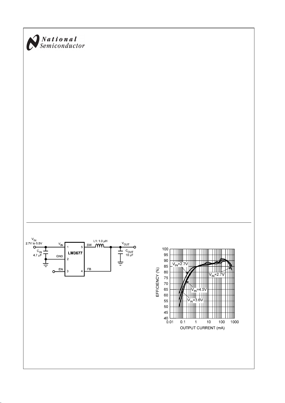
Typical Application Circuit
30008401
FIGURE 1. Typical Application Circuit
Efficiency vs. Output Current
(V
OUT
= 1.8V)
30008487
© 2007 National Semiconductor Corporation 300084 www.national.com
LM3677 3MHz, 600mA Miniature Step-Down DC-DC Converter for Ultra Low Voltage Circuits
Page 2
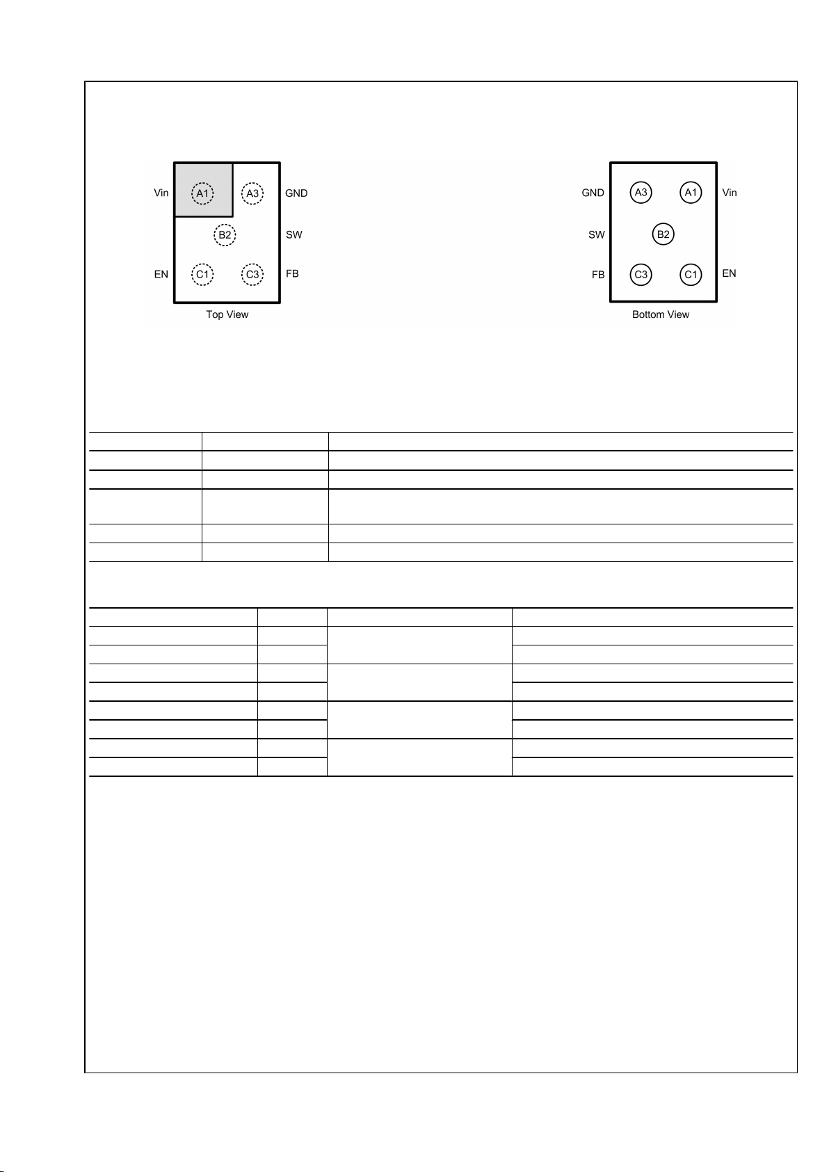
Connection Diagram and Package Mark Information
5-Bump micro SMD Package NS Package Number TLA05FEA
30008444
FIGURE 2. 5 Bump Micro SMD Package
Pin Descriptions
Pin # Name Description
A1 V
IN
Power supply input. Connect to the input filter capacitor (Figure 1).
A3 GND Ground pin.
C1 EN Enable pin. The device is in shutdown mode when voltage to this pin is <0.4V and enabled
when >1.0V. Do not leave this pin floating.
C3 FB Feedback analog input. Connect directly to the output filter capacitor ( FIGURE 1).
B2 SW Switching node connection to the internal PFET switch and NFET synchronous rectifier.
Ordering Information
Order Number Spec Package Marking Supplied As
LM3677TL-1.3 NOPB
V
250 units, Tape-and-Reel
LM3677TLX-1.3 NOPB 3000 units, Tape-and-Reel
LM3677TL-1.5 NOPB
X
250 units, Tape-and-Reel
LM3677TLX-1.5 NOPB 3000 units, Tape-and-Reel
LM3677TL-1.8 NOPB
Y
250 units, Tape-and-Reel
LM3677TLX-1.8 NOPB 3000 units, Tape-and-Reel
LM3677TL-2.5 NOPB
Z
250 units, Tape-and-Reel
LM3677TLX-2.5 NOPB 3000 units, Tape-and-Reel
Note: 1.2V, 1.6V, 2.8V and ADJ are coming soon.
www.national.com 2
LM3677
Page 3
Absolute Maximum Ratings (Note 1)
If Military/Aerospace specified devices are required,
please contact the National Semiconductor Sales Office/
Distributors for availability and specifications.
If Military/Aerospace specified devices are required, please
contact the National Semiconductor Sales Office/Distributors
for availability and specifications.
VIN Pin: Voltage to GND −0.2V to 6.0V
FB, SW, EN Pin: (GND−0.2V) to
(VIN + 0.2V)
Continuous Power Dissipation
(Note 3)
Internally Limited
Junction Temperature (T
J-MAX
) +125°C
Storage Temperature Range −65°C to +150°C
Maximum Lead Temperature
(Soldering, 10 sec.)
260°C
ESD Rating (Note 4)
Human Body Model: All Pins 2.0 kV
Machine Model: All Pins 200V
Operating Ratings (Note 1), (Note 2)
Input Voltage Range 2.7V to 5.5V
Recommended Load Current 0mA to 600 mA
Junction Temperature (TJ) Range −30°C to +125°C
Ambient Temperature (TA) Range (Note5)−30°C to +85°C
Thermal Properties
Junction-to-Ambient Thermal
Resistance (θJA) (Note 6)
85°C/W
Electrical Characteristics (Note 2), (Note 8), (Note 9) Limits in standard typeface are for T
J
= TA = 25°C.
Limits in boldface type apply over the operating ambient temperature range (−30°C ≤ TA ≤ +85°C). Unless otherwise noted,
specifications apply to the LM3677 with VIN = EN = 3.6V.
Symbol Parameter Condition Min Typ Max Units
V
IN
Input Voltage 2.7 5.5 V
V
FB
Feedback Voltage PWM mode -2.5 +2.5 %
V
REF
Internal Reference Voltage 0.5 V
I
SHDN
Shutdown Supply Current EN = 0V 0.01 1 µA
I
Q
DC Bias Current into V
IN
No load, device is not switching 16 35 µA
R
DSON (P)
Pin-Pin Resistance for PFET VIN= VGS= 3.6V, ISW= 100mA 350 450
mΩ
R
DSON (N)
Pin-Pin Resistance for NFET VIN= VGS= 3.6V, ISW= -100mA 150 250
mΩ
I
LIM
Switch Peak Current Limit Open Loop(Note 7) 1085 1220 1375 mA
V
IH
Logic High Input 1.0 V
V
IL
Logic Low Input 0.4 V
I
EN
Enable (EN) Input Current 0.01 1 µA
F
OSC
Internal Oscillator Frequency PWM Mode 2.5 3 3.5 MHz
Note 1: Absolute Maximum Ratings indicate limits beyond which damage to the component may occur. Operating Ratings are conditions under which operation
of the device is guaranteed. Operating Ratings do not imply guaranteed performance limits. For guaranteed performance limits and associated test conditions,
see the Electrical Characteristics tables.
Note 2: All voltages are with respect to the potential at the GND pin.
Note 3: Internal thermal shutdown circuitry protects the device from permanent damage. Thermal shutdown engages at TJ= 150°C (typ.) and disengages at
TJ= 130°C (typ.).
Note 4: The Human body model is a 100 pF capacitor discharged through a 1.5 kΩ resistor into each pin. The machine model is a 200 pF capacitor discharged
directly into each pin. MIL-STD-883 3015.7
Note 5: In Applications where high power dissipation and/or poor package resistance is present, the maximum ambient temperature may have to be derated.
Maximum ambient temperature (T
A-MAX
) is dependent on the maximum operating junction temperature (T
J-MAX
), the maximum power dissipation of the device in
the application (P
D-MAX
) and the junction to ambient thermal resistance of the package (θJA) in the application, as given by the following equation: T
A-MAX
= T
J-MAX
− (θJAx P
D-MAX
). Refer to Dissipation rating table for P
D-MAX
values at different ambient temperatures.
Note 6: Junction to ambient thermal resistance is highly application and board layout dependent. In applications where high power dissipation exists, special care
must be given to thermal dissipation issues in board design. Value specified here 85 °C/W is based on measurement results using a 4 layer board as per JEDEC
standards.
Note 7: Refer to datasheet curves for closed loop data and its variation with regards to supply voltage and temperature. Electrical Characteristic table reflects
open loop data (FB=0V and current drawn from SW pin ramped up until cycle by cycle current limit is activated). Closed loop current limit is the peak inductor
current measured in the application circuit by increasing output current until output voltage drops by 10%.
Note 8: Min and Max limits are guaranteed by design, test or statistical analysis. Typical numbers are not guaranteed, but do represent the most likely norm.
Note 9: The parameters in the electrical characteristic table are tested under open loop conditions at VIN= 3.6V unless otherwise specified. For performance over
the input voltage range and closed loop condition, refer to the datasheet curves.
3 www.national.com
LM3677
Page 4
Dissipation Rating Table
θ
JA
T
A
≤ 25°C
Power Rating
TA= 60°C
Power Rating
TA= 85°C
Power Rating
85°C/W (4-layer board) 1176 mW 765 mW 470 mW
www.national.com 4
LM3677
Page 5
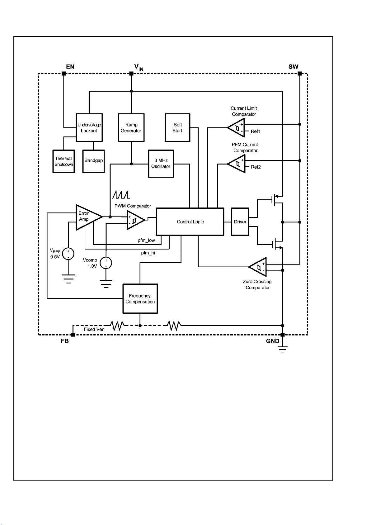
Block Diagram
30008418
FIGURE 3. Simplified Functional Diagram
5 www.national.com
LM3677
Page 6
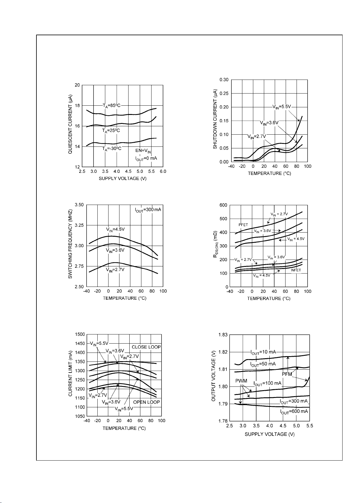
Typical Performance Characteristics
LM3677TL, Circuit of Figure 1, VIN = 3.6V, V
OUT
= 1.8V, TA = 25°C, unless otherwise noted.
Quiescent Supply Current vs. Supply Voltage
(Switching)
30008481
Shutdown Current vs. Temp
30008482
Switching Frequency vs. Temperature
30008483
R
DS(ON)
vs. Temperature
30008451
Open/Closed Loop Current Limit
vs. Temperature
30008449
Output Voltage vs. Supply Voltage
(V
OUT
= 1.8V)
30008484
www.national.com 6
LM3677
Page 7

Output Voltage vs. Supply Voltage
(V
OUT
= 2.5V)
30008438
Output Voltage vs. Temperature
(V
OUT
= 1.3V)
30008468
Output Voltage vs. Temperature
(V
OUT
= 1.8V)
30008485
Output Voltage vs. Temperature
(V
OUT
= 2.5V)
30008469
Output Voltage vs. Output Current
(V
OUT
= 1.8V)
30008486
Output Voltage vs. Output Current
(V
OUT
= 2.5V)
30008437
7 www.national.com
LM3677
Page 8

Efficiency vs. Output Current
(V
OUT
= 1.3V)
30008441
Efficiency vs. Output Current
(V
OUT
= 1.8V)
30008487
Efficiency vs. Output Current
(V
OUT
= 2.5V)
30008432
Output Current vs. Input Voltage at Mode Change Point
(V
OUT
= 1.3V)
30008435
Output Current vs. Input Voltage at Mode Change Point
(V
OUT
= 1.8V)
30008488
Output Current vs. Input Voltage at Mode Change Point
(V
OUT
= 2.5V)
30008436
www.national.com 8
LM3677
Page 9

Line Transient Response
V
OUT
= 1.3V (PWM Mode)
30008433
Line Transient Response
V
OUT
= 1.8V (PWM Mode)
30008477
Line Transient Response
V
OUT
= 1.8V (PWM Mode)
30008478
Line Transient Response
V
OUT
= 2.5V (PWM Mode)
30008439
Load Transient Response (V
OUT
= 1.3V)
(PFM Mode 1mA to 50mA)
30008493
Load Transient Response (V
OUT
= 1.3V)
(PFM Mode 50mA to 1mA)
30008494
9 www.national.com
LM3677
Page 10

Load Transient Response (V
OUT
= 1.8V)
(PFM Mode 1mA to 50mA)
30008473
Load Transient Response (V
OUT
= 1.8V)
(PFM Mode 50mA to 1mA)
30008474
Load Transient Response (V
OUT
= 2.5V)
(PFM Mode 1mA to 50mA)
30008498
Load Transient Response (V
OUT
= 2.5V)
(PFM Mode 50mA to 1mA)
30008430
Mode Change by Load Transients
V
OUT
= 1.3V (PFM to PWM)
30008495
Mode Change by Load Transients
V
OUT
= 1.3V (PWM to PFM)
30008496
www.national.com 10
LM3677
Page 11

Mode Change by Load Transients
V
OUT
= 1.8V (PFM to PWM)
30008475
Mode Change by Load Transients
V
OUT
= 1.8V (PWM to PFM)
30008476
Load Transient Response
V
OUT
= 1.3V (PWM Mode)
30008497
Load Transient Response
V
OUT
= 1.8V (PWM Mode)
30008472
Load Transient Response
V
OUT
= 2.5V (PWM Mode)
30008431
Start Up into PWM Mode
V
OUT
= 1.3V (Output Current= 300mA)
30008491
11 www.national.com
LM3677
Page 12

Start Up into PFM Mode
V
OUT
= 1.3V (Output Current= 1mA)
30008492
Start Up into PWM Mode
V
OUT
= 1.8V (Output Current= 300mA)
30008470
Start Up into PFM Mode
V
OUT
= 1.8V (Output Current= 1mA)
30008471
Start Up into PWM Mode
V
OUT
= 2.5V (Output Current= 300mA)
30008489
Start Up into PFM Mode
V
OUT
= 2.5V (Output Current= 1mA)
30008490
www.national.com 12
LM3677
Page 13

Operation Description
DEVICE INFORMATION
The LM3677, a high efficiency step down DC-DC switching
buck converter, delivers a constant voltage from a single LiIon battery and input voltage rails from 2.7V to 5.5V such as
cell phones and PDAs. Using a voltage mode architecture
with synchronous rectification, the LM3677 has the ability to
deliver up to 600mA depending on the input voltage and output voltage, ambient temperature, and the inductor chosen.
There are three modes of operation depending on the current
required - PWM (Pulse Width Modulation), PFM (Pulse Frequency Modulation), and shutdown. The device operates in
PWM mode at load current of approximately 80 mA or higher,
having a voltage precision of ±2.5% with 90% efficiency or
better. Lighter load current causes the device to automatically
switch into PFM mode for reduced current consumption (IQ =
16 µA typ) and a longer battery life. Shutdown mode turns off
the device, offering the lowest current consumption
(I
SHUTDOWN
= 0.01 µA typ).
Additional features include soft-start, under voltage protection, current overload protection, and thermal shutdown protection. As shown in Figure 1, only three external power
components are required for implementation.
The part uses an internal reference voltage of 0.5V. It is recommended to keep the part in shutdown until the input voltage
exceeds 2.7V.
CIRCUIT OPERATION
The LM3677 operates as follows. During the first portion of
each switching cycle, the control block in the LM3677 turns
on the internal PFET switch. This allows current to flow from
the input through the inductor to the output filter capacitor and
load. The inductor limits the current to a ramp with a slope of
(VIN–V
OUT
)/L, by storing energy in a magnetic field.
During the second portion of each cycle, the controller turns
the PFET switch off, blocking current flow from the input, and
then turns the NFET synchronous rectifier on. The inductor
draws current from ground through the NFET to the output
filter capacitor and load, which ramps the inductor current
down with a slope of - V
OUT
/L.
The output filter stores charge when the inductor current is
high, and releases it when inductor current is low, smoothing
the voltage across the load.
The output voltage is regulated by modulating the PFET
switch on time to control the average current sent to the load.
The effect is identical to sending a duty-cycle modulated rectangular wave formed by the switch and synchronous rectifier
at the SW pin to a low-pass filter formed by the inductor and
output filter capacitor. The output voltage is equal to the average voltage at the SW pin.
PWM OPERATION
During PWM operation, the converter operates as a voltagemode controller with input voltage feed forward. This allows
the converter to achieve good load and line regulation. The
DC gain of the power stage is proportional to the input voltage.
To eliminate this dependence, feed forward inversely proportional to the input voltage is introduced.
While in PWM mode, the output voltage is regulated by
switching at a constant frequency and then modulating the
energy per cycle to control power to the load. At the beginning
of each clock cycle the PFET switch is turned on and the inductor current ramps up until the comparator trips and the
control logic turns off the switch. The current limit comparator
can also turn off the switch in case the current limit of the
PFET is exceeded. Then the NFET switch is turned on and
the inductor current ramps down. The next cycle is initiated
by the clock turning off the NFET and turning on the PFET.
30008480
FIGURE 4. Typical PWM Operation
Internal Synchronous Rectification
While in PWM mode, the LM3677 uses an internal NFET as
a synchronous rectifier to reduce rectifier forward voltage
drop and associated power loss. Synchronous rectification
provides a significant improvement in efficiency whenever the
output voltage is relatively low compared to the voltage drop
across an ordinary rectifier diode.
Current Limiting
A current limit feature allows the LM3677 to protect itself and
external components during overload conditions. PWM mode
implements current limiting using an internal comparator that
trips at 1220 mA (typ). If the output is shorted to ground the
device enters a timed current limit mode where the NFET is
turned on for a longer duration until the inductor current falls
below a low threshold, ensuring inductor current has more
time to decay, thereby preventing runaway.
PFM OPERATION
At very light loads, the converter enters PFM mode and operates with reduced switching frequency and supply current
to maintain high efficiency.
The part will automatically transition into PFM mode when either of the following conditions occurs for a duration of 32 or
more clock cycles:
A. The NFET current reaches zero.
B. The peak PMOS switch current drops below the I
MODE
level, (Typically I
MODE
< 75mA + VIN/55 Ω ).
13 www.national.com
LM3677
Page 14

30008479
FIGURE 5. Typical PFM Operation
During PFM operation, the converter positions the output voltage slightly higher than the nominal output voltage during
PWM operation allowing additional headroom for voltage
drop during a load transient from light to heavy load. The PFM
comparators sense the output voltage via the feedback pin
and control the switching of the output FETs such that the
output voltage ramps between ~0.2% and ~1.8% above the
nominal PWM output voltage. If the output voltage is below
the ‘high’ PFM comparator threshold, the PMOS power switch
is turned on. It remains on until the output voltage reaches the
‘high’ PFM threshold or the peak current exceeds the I
PFM
level set for PFM mode. The typical peak current in PFM mode
is: I
PFM
= 112mA + VIN/20Ω .
Once the PMOS power switch is turned off, the NMOS power
switch is turned on until the inductor current ramps to zero.
When the NMOS zero-current condition is detected, the
NMOS power switch is turned off. If the output voltage is below the ‘high’ PFM comparator threshold (see Figure 6), the
PMOS switch is again turned on and the cycle is repeated
until the output reaches the desired level. Once the output
reaches the ‘high’ PFM threshold, the NMOS switch is turned
on briefly to ramp the inductor current to zero and then both
output switches are turned off and the part enters an extremely low power mode. Quiescent supply current during this
‘sleep’ mode is 16µA (typ), which allows the part to achieve
high efficiencies under extremely light load conditions.
If the load current should increase during PFM mode (Figure
6) causing the output voltage to fall below the ‘low2’ PFM
threshold, the part will automatically transition into fixed-frequency PWM mode. When V
IN
=2.7V the part transitions from
PWM to PFM mode at ~ 35mA output current and from PFM
to PWM mode at ~ 95mA , when VIN=3.6V, PWM to PFM
transition occurs at ~ 42mA and PFM to PWM transition occurs at ~ 115mA, when VIN =4.5V, PWM to PFM transition
occurs at ~ 60mA and PFM to PWM transition occurs at ~
135mA.
30008403
FIGURE 6. Operation in PFM Mode and Transfer to PWM Mode
SHUTDOWN MODE
Setting the EN input pin low (<0.4V) places the LM3677 in
shutdown mode. During shutdown the PFET switch, NFET
switch, reference, control and bias circuitry of the LM3677 are
turned off. Setting EN high (>1.0V) enables normal operation.
It is recommended to set EN pin low to turn off the LM3677
during system power up and undervoltage conditions when
the supply is less than 2.7V. Do not leave the EN pin floating.
SOFT START
The LM3677 has a soft-start circuit that limits in-rush current
during start-up. During start-up the switch current limit is increased in steps. Soft start is activated only if EN goes from
logic low to logic high after Vin reaches 2.7V. Soft start is implemented by increasing switch current limit in steps of 200mA, 400mA, 600mA and 1220mA (typical switch current
limit). The start-up time thereby depends on the output capacitor and load current demanded at start-up. Typical start-
www.national.com 14
LM3677
Page 15

up times with a 10µF output capacitor and 300mA load is 300
µs and with 1mA load is 200µs.
Application Information
INDUCTOR SELECTION
There are two main considerations when choosing an inductor; the inductor should not saturate, and the inductor current
ripple should be small enough to achieve the desired output
voltage ripple. Different saturation current rating specifications are followed by different manufacturers so attention
must be given to details. Saturation current ratings are typically specified at 25°C. However, ratings at the maximum
ambient temperature of application should be requested form
the manufacturer. The minimum value of inductance to
guarantee good performance is 0.7µH at I
LIM
(typ) dc cur-
rent over the ambient temperature range. Shielded induc-
tors radiate less noise and should be preferred.
There are two methods to choose the inductor saturation cur-
rent rating.
Method 1:
The saturation current is greater than the sum of the maximum load current and the worst case average to peak inductor current. This can be written as
•
I
RIPPLE
: average to peak inductor current
•
I
OUTMAX
: maximum load current (600mA)
•
VIN: maximum input voltage in application
•
L : min inductor value including worst case tolerances
(30% drop can be considered for method 1)
•
f : minimum switching frequency (2.5MHz)
•
V
OUT
: output voltage
Method 2:
A more conservative and recommended approach is to
choose an inductor that has saturation current rating greater
than the max current limit of 1375mA.
A 1.0 µH inductor with a saturation current rating of at least
1375 mA is recommended for most applications. The
inductor’s resistance should be less than 0.15Ω for good efficiency. Table 1 lists suggested inductors and suppliers. For
low-cost applications, an unshielded bobbin inductor could be
considered. For noise critical applications, a toroidal or shielded-bobbin inductor should be used. A good practice is to lay
out the board with overlapping footprints of both types for design flexibility. This allows substitution of a low-noise shielded
inductor in the event that noise from low-cost bobbin models
is unacceptable.
INPUT CAPACITOR SELECTION
A ceramic input capacitor of 4.7 µF, 6.3V is sufficient for most
applications. Place the input capacitor as close as possible to
the VIN pin of the device. A larger value may be used for improved input voltage filtering. Use X7R or X5R types; do not
use Y5V. DC bias characteristics of ceramic capacitors must
be considered when selecting case sizes like 0603 and 0805.
The minimum input capacitance to guarantee good performance is 2.2µF at 3V dc bias; 1.5µF at 5V dc bias
including tolerances and over ambient temperature
range. The input filter capacitor supplies current to the PFET
switch of the LM3677 in the first half of each cycle and reduces voltage ripple imposed on the input power source. A
ceramic capacitor’s low ESR provides the best noise filtering
of the input voltage spikes due to this rapidly changing current. Select a capacitor with sufficient ripple current rating.
The input current ripple can be calculated as:
15 www.national.com
LM3677
Page 16

TABLE 1. Suggested Inductors and Their Suppliers
Model Vendor Dimensions LxWxH(mm) D.C.R (max)
MIPSA2520D 1R0 FDK 2.5 x 2.0 x 1.2
100 mΩ
LQM2HP 1R0 Murata 2.5 x 2.0 x 0.95
100 mΩ
BRL2518T1R0M Taiyo Yuden 2.5x 1.8 x 1.2
80 mΩ
OUTPUT CAPACITOR SELECTION
A ceramic output capacitor of 10 µF, 6.3V is sufficient for most
applications. Use X7R or X5R types; do not use Y5V. DC bias
characteristics of ceramic capacitors must be considered
when selecting case sizes like 0603 and 0805. DC bias characteristics vary from manufacturer to manufacturer and dc
bias curves should be requested from them as part of the capacitor selection process.
The minimum output capacitance to guarantee good performance is 5.75µF at 2.5V dc bias including tolerances
and over ambient temperature range. The output filter ca-
pacitor smoothes out current flow from the inductor to the
load, helps maintain a steady output voltage during transient
load changes and reduces output voltage ripple. These capacitors must be selected with sufficient capacitance and
sufficiently low ESR to perform these functions.
The output voltage ripple is caused by the charging and discharging of the output capacitor and by the R
ESR
and can be
calculated as:
Voltage peak-to-peak ripple due to capacitance can be ex-
pressed as follows
Voltage peak-to-peak ripple due to ESR can be expressed as
follows
V
PP-ESR
= (2 * I
RIPPLE
) * R
ESR
Because these two components are out of phase the rms (root
mean squared) value can be used to get an approximate value of peak-to-peak ripple.
Voltage peak-to-peak ripple,rms can be expressed as follow:
Note that the output voltage ripple is dependent on the inductor current ripple and the equivalent series resistance of the
output capacitor (R
ESR
).
The R
ESR
is frequency dependent (as well as temperature
dependent); make sure the value used for calculations is at
the switching frequency of the part.
TABLE 2. Suggested Capacitors and Their Suppliers
Model Type Vendor Voltage Rating
Case Size
Inch (mm)
4.7 µF for C
IN
C1608X5R0J475 Ceramic, X5R TDK 6.3V 0603 (1608)
C2012X5R0J475 Ceramic, X5R TDK 6.3V 0805 (2012)
GRM21BR60J475 Ceramic, X5R muRata 6.3V 0805 (2012)
JMK212BJ475 Ceramic, X5R Taiyo-Yuden 6.3V 0805 (2012)
10 µF for C
OUT
C1608X5R0J106 Ceramic, X5R TDK 6.3V 0603 (1608)
C2012X5R0J106 Ceramic, X5R TDK 6.3V 0805 (2012)
GRM21BR60J106 Ceramic, X5R muRata 6.3V 0805 (2012)
JMK212BJ106 Ceramic, X5R Taiyo-Yuden 6.3V 0805 (2012)
Micro SMD PACKAGE ASSEMBLY AND USE
Use of the Micro SMD package requires specialized board
layout, precision mounting and careful re-flow techniques, as
detailed in National Semiconductor Application Note 1112.
Refer to the section "Surface Mount Technology (SMD) Assembly Considerations". For best results in assembly, alignment ordinals on the PC board should be used to facilitate
placement of the device. The pad style used with Micro SMD
package must be the NSMD (non-solder mask defined) typ.
This means that the solder-mask opening is larger than the
pad size. This prevents a lip that otherwise forms if the soldermask and pad overlap, from holding the device off the surface
of the board and interfering with mounting. See Application
Note 1112 for specific instructions how to do this. The 5-Bump
package used for LM3677 has 300 micron solder balls and
requires 10.82 mils pads for mounting on the circuit board.
The trace to each pad should enter the pad with a 90° entry
angle to prevent debris from being caught in deep corners.
Initially, the trace to each pad should be 7 mil wide, for a section approximately 7 mil long or longer, as a thermal relief.
Then each trace should neck up or down to its optimal width.
The important criteria is symmetry. This ensures the solder
bumps on the LM3677 re-flow evenly and that the device solders level to the board. In particular, special attention must be
paid to the pads for bumps A1 and A3, because GND and
VIN are typically connected to large copper planes, inadequate thermal relief can result in late or inadequate re-flow of
these bumps.
www.national.com 16
LM3677
Page 17

The Micro SMD package is optimized for the smallest possible size in applications with red or infrared opaque cases.
Because the Micro SMD package lacks the plastic encapsulation characteristic of larger devices, it is vulnerable to light.
Backside metallization and/or epoxy coating, along with frontside shading by the printed circuit board, reduce this sensitivity. However, the package has exposed die edges. In
particular, Micro SMD devices are sensitive to light, in the red
and infrared range, shining on the package’s exposed die
edges.
BOARD LAYOUT CONSIDERATIONS
PC board layout is an important part of DC-DC converter design. Poor board layout can disrupt the performance of a DCDC converter and surrounding circuitry by contributing to EMI,
ground bounce, and resistive voltage loss in the traces. These
can send erroneous signals to the DC-DC converter IC, resulting in poor regulation or instability. Poor layout can also
result in re-flow problems leading to poor solder joints between the Micro SMD package and board pads. Poor solder
joints can result in erratic or degraded performance.
30008454
FIGURE 7. Board Layout Design Rules for the LM3677
Good layout for the LM3677 can be implemented by following
a few simple design rules, as illustrated in Figure.
1.
Place the LM3677 on 10.82 mil pads. As a thermal relief,
connect to each pad with a 7 mil wide, approximately 7
mil long trace, and then incrementally increase each
trace to its optimal width. The important criterion is
symmetry to ensure the solder bumps on the re-flow
evenly (see Micro SMD Package Assembly and Use).
2.
Place the LM3677, inductor and filter capacitors close
together and make the traces short. The traces between
these components carry relatively high switching
currents and act as antennas. Following this rule reduces
radiated noise. Special care must be given to place the
input filter capacitor very close to the VIN and GND pin.
3.
Arrange the components so that the switching current
loops curl in the same direction. During the first half of
each cycle, current flows from the input filter capacitor,
through the LM3677 and inductor to the output filter
capacitor and back through ground, forming a current
loop. In the second half of each cycle, current is pulled
up from ground, through the LM3677 by the inductor, to
the output filter capacitor and then back through ground,
forming a second current loop. Routing these loops so
the current curls in the same direction prevents magnetic
field reversal between the two half-cycles and reduces
radiated noise.
4.
Connect the ground pins of the LM3677, and filter
capacitors together using generous component-side
copper fill as a pseudo-ground plane. Then connect this
to the ground-plane (if one is used) with several vias. This
reduces ground-plane noise by preventing the switching
currents from circulating through the ground plane. It also
reduces ground bounce at the LM3677 by giving it a lowimpedance ground connection.
5.
Use wide traces between the power components and for
power connections to the DC-DC converter circuit. This
reduces voltage errors caused by resistive losses across
the traces
6.
Route noise sensitive traces such as the voltage
feedback pathaway from noisy traces between the power
components. The voltage feedback trace must remain
close to the LM3677 circuit and should be routed directly
from FB to V
OUT
at the output capacitor and should be
routed opposite to noise components. This reduces EMI
radiated onto the DC-DC converter’s own voltage
feedback trace.
17 www.national.com
LM3677
Page 18

7.
Place noise sensitive circuitry, such as radio IF blocks,
away from the DC-DC converter, CMOS digital blocks
and other noisy circuitry. Interference with noisesensitive circuitry in the system can be reduced through
distance.
In mobile phones, for example, a common practice is to place
the DC-DC converter on one corner of the board, arrange the
CMOS digital circuitry around it (since this also generates
noise), and then place sensitive preamplifiers and IF stages
on the diagonally opposing corner. Often, the sensitive circuitry is shielded with a metal pan and power to it is postregulated to reduce conducted noise, using low-dropout
linear regulators.
www.national.com 18
LM3677
Page 19

Physical Dimensions inches (millimeters) unless otherwise noted
5-Bump (Large) Micro SMD Package, 0.5mm Pitch
NS Package Number TLA05FEA
The dimensions for X1, X2, and X3 are as given:
X1 = 1.107 mm +/- 0.030mm
X2 = 1.488 mm +/- 0.030mm
X3 = 0.600 mm +/- 0.075mm
19 www.national.com
LM3677
Page 20

Notes
LM3677 3MHz, 600mA Miniature Step-Down DC-DC Converter for Ultra Low Voltage Circuits
THE CONTENTS OF THIS DOCUMENT ARE PROVIDED IN CONNECTION WITH NATIONAL SEMICONDUCTOR CORPORATION
(“NATIONAL”) PRODUCTS. NATIONAL MAKES NO REPRESENTATIONS OR WARRANTIES WITH RESPECT TO THE ACCURACY
OR COMPLETENESS OF THE CONTENTS OF THIS PUBLICATION AND RESERVES THE RIGHT TO MAKE CHANGES TO
SPECIFICATIONS AND PRODUCT DESCRIPTIONS AT ANY TIME WITHOUT NOTICE. NO LICENSE, WHETHER EXPRESS,
IMPLIED, ARISING BY ESTOPPEL OR OTHERWISE, TO ANY INTELLECTUAL PROPERTY RIGHTS IS GRANTED BY THIS
DOCUMENT.
TESTING AND OTHER QUALITY CONTROLS ARE USED TO THE EXTENT NATIONAL DEEMS NECESSARY TO SUPPORT
NATIONAL’S PRODUCT WARRANTY. EXCEPT WHERE MANDATED BY GOVERNMENT REQUIREMENTS, TESTING OF ALL
PARAMETERS OF EACH PRODUCT IS NOT NECESSARILY PERFORMED. NATIONAL ASSUMES NO LIABILITY FOR
APPLICATIONS ASSISTANCE OR BUYER PRODUCT DESIGN. BUYERS ARE RESPONSIBLE FOR THEIR PRODUCTS AND
APPLICATIONS USING NATIONAL COMPONENTS. PRIOR TO USING OR DISTRIBUTING ANY PRODUCTS THAT INCLUDE
NATIONAL COMPONENTS, BUYERS SHOULD PROVIDE ADEQUATE DESIGN, TESTING AND OPERATING SAFEGUARDS.
EXCEPT AS PROVIDED IN NATIONAL’S TERMS AND CONDITIONS OF SALE FOR SUCH PRODUCTS, NATIONAL ASSUMES NO
LIABILITY WHATSOEVER, AND NATIONAL DISCLAIMS ANY EXPRESS OR IMPLIED WARRANTY RELATING TO THE SALE
AND/OR USE OF NATIONAL PRODUCTS INCLUDING LIABILITY OR WARRANTIES RELATING TO FITNESS FOR A PARTICULAR
PURPOSE, MERCHANTABILITY, OR INFRINGEMENT OF ANY PATENT, COPYRIGHT OR OTHER INTELLECTUAL PROPERTY
RIGHT.
LIFE SUPPORT POLICY
NATIONAL’S PRODUCTS ARE NOT AUTHORIZED FOR USE AS CRITICAL COMPONENTS IN LIFE SUPPORT DEVICES OR
SYSTEMS WITHOUT THE EXPRESS PRIOR WRITTEN APPROVAL OF THE CHIEF EXECUTIVE OFFICER AND GENERAL
COUNSEL OF NATIONAL SEMICONDUCTOR CORPORATION. As used herein:
Life support devices or systems are devices which (a) are intended for surgical implant into the body, or (b) support or sustain life and
whose failure to perform when properly used in accordance with instructions for use provided in the labeling can be reasonably expected
to result in a significant injury to the user. A critical component is any component in a life support device or system whose failure to perform
can be reasonably expected to cause the failure of the life support device or system or to affect its safety or effectiveness.
National Semiconductor and the National Semiconductor logo are registered trademarks of National Semiconductor Corporation. All other
brand or product names may be trademarks or registered trademarks of their respective holders.
Copyright© 2007 National Semiconductor Corporation
For the most current product information visit us at www.national.com
National Semiconductor
Americas Customer
Support Center
Email:
new.feedback@nsc.com
Tel: 1-800-272-9959
National Semiconductor Europe
Customer Support Center
Fax: +49 (0) 180-530-85-86
Email: europe.support@nsc.com
Deutsch Tel: +49 (0) 69 9508 6208
English Tel: +49 (0) 870 24 0 2171
Français Tel: +33 (0) 1 41 91 8790
National Semiconductor Asia
Pacific Customer Support Center
Email: ap.support@nsc.com
National Semiconductor Japan
Customer Support Center
Fax: 81-3-5639-7507
Email: jpn.feedback@nsc.com
Tel: 81-3-5639-7560
www.national.com
 Loading...