

Page 1
July 2007
LM3668
1A, High Efficiency Dual Mode Single Inductor Buck-Boost
DC/DC Converter
General Description
The LM3668 is a synchornous buck-boost DC-DC converter
optimized for powering low voltage circuits from a Li-Ion battery and input voltage rails between 2.5V and 5.5V. It has the
capability to support up to 1A output current over a output
voltage range of 2.8V/3.3V. The LM3668 regulates the output
voltage over the complete input voltage range by automatically switching between buck or boost modes depending on
the input voltage.
The LM3668 has 2 N-channel MOSFETS and 2 P-channel
MOSFETS arranged in a topology that provides continuous
operation through the buck and boost operating modes.
There is a MODE pin that allows the user to choose between
an intelligent automatic PFM-PWM mode operation and
forced PWM operation. During PWM mode, a fixed-frequency
2.2MHz (typ.) is used. PWM mode drives load up to 1A. Hysteretic PFM mode extends the battery life through reduction
of the quiescent current to 45µA (typ.) at light loads during
system standby. Internal synchronous rectification provides
high efficiency. In shutdown mode (Enable pin pulled low) the
device turns off and reduces battery consumption to 0.01µA
(typ.).
The LM3668 is available in a 12-pin LLP package. A high
switching frequency of 2.2MHz (typ.) allows the use of tiny
surface-mount components including a 2.2µH inductor, a
10µF input capacitor, and a 22µF output capacitor.
Features
■
45µA typical quiescent current
■
1A maximum load current for VIN = 2.8V to 5.5V
■
800mA maximum load current for VIN = 2.7V
■
600mA maximum load current for VIN = 2.5V
■
2.2 MHz PWM fixed switching frequency (typ.)
■
Automatic PFM-PWM Mode or Forced PWM Mode
■
Wide Input Voltage Range: 2.5V to 5.5V
■
Output Voltage Range: 2.8V/3.3V
■
Internal synchronous rectification for high efficiency
■
Internal soft start: 600µs Maximum start-up time
■
0.01µA typical shutdown current
■
Current overload and Thermal shutdown protection
■
Frequency Sync Pin: 1.6Mhz to 2.7MHz
Applications
■
Handset Peripherals
■
MP3 players
■
Pre-Regulation for linear regulators
■
PDAs
■
Portable Hard Disk Drives
■
WiMax Modems
Typical Applications
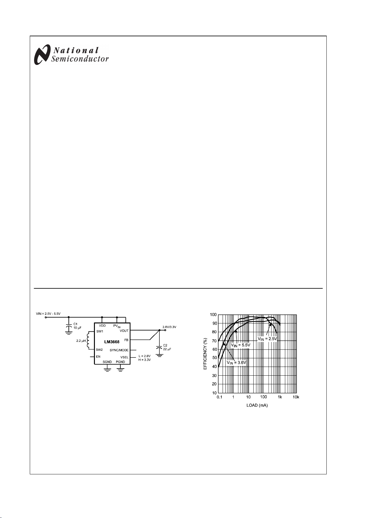
20191401
Typical Application Circuit
20191425
Efficiency at 3.3V Output
© 2007 National Semiconductor Corporation 201914 www.national.com
LM3668 1A, High Efficiency Dual Mode Single Inductor Buck-Boost DC/DC Converter
Page 2
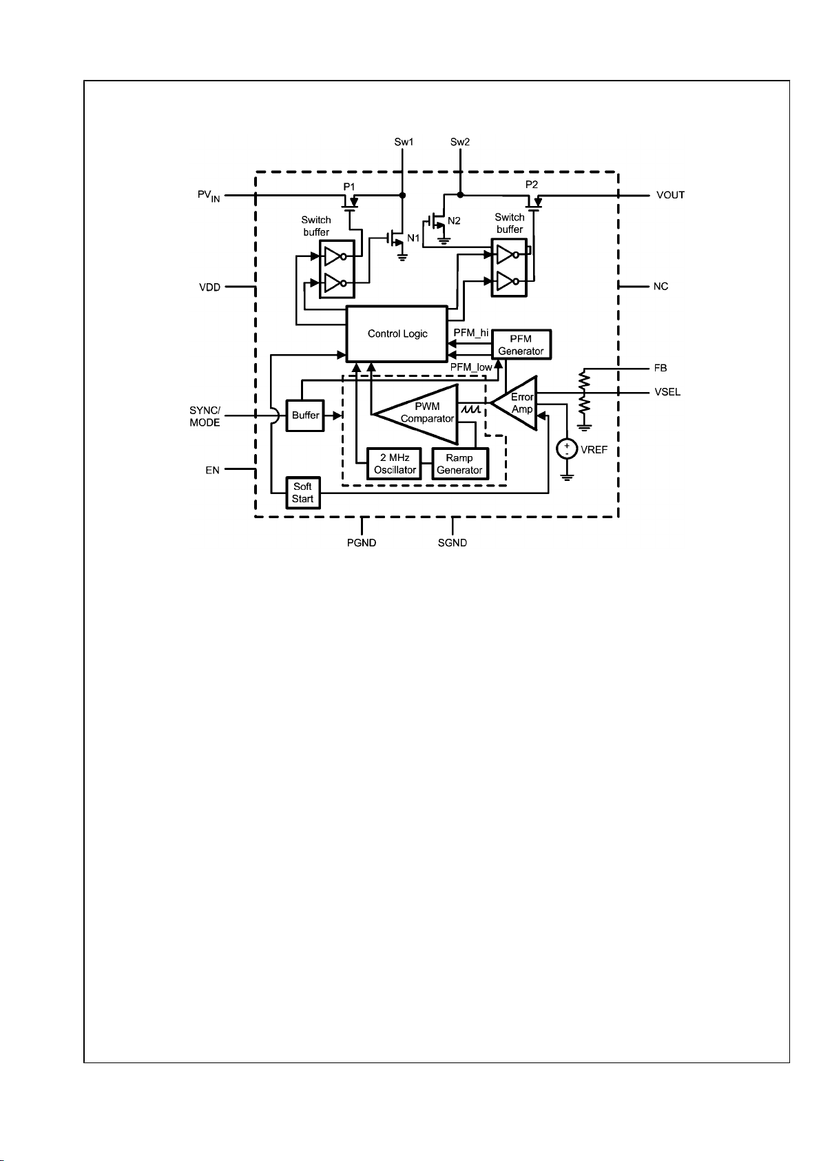
Functional Block Diagram
20191404
FIGURE 1. Functional Block Diagram
www.national.com 2
LM3668
Page 3
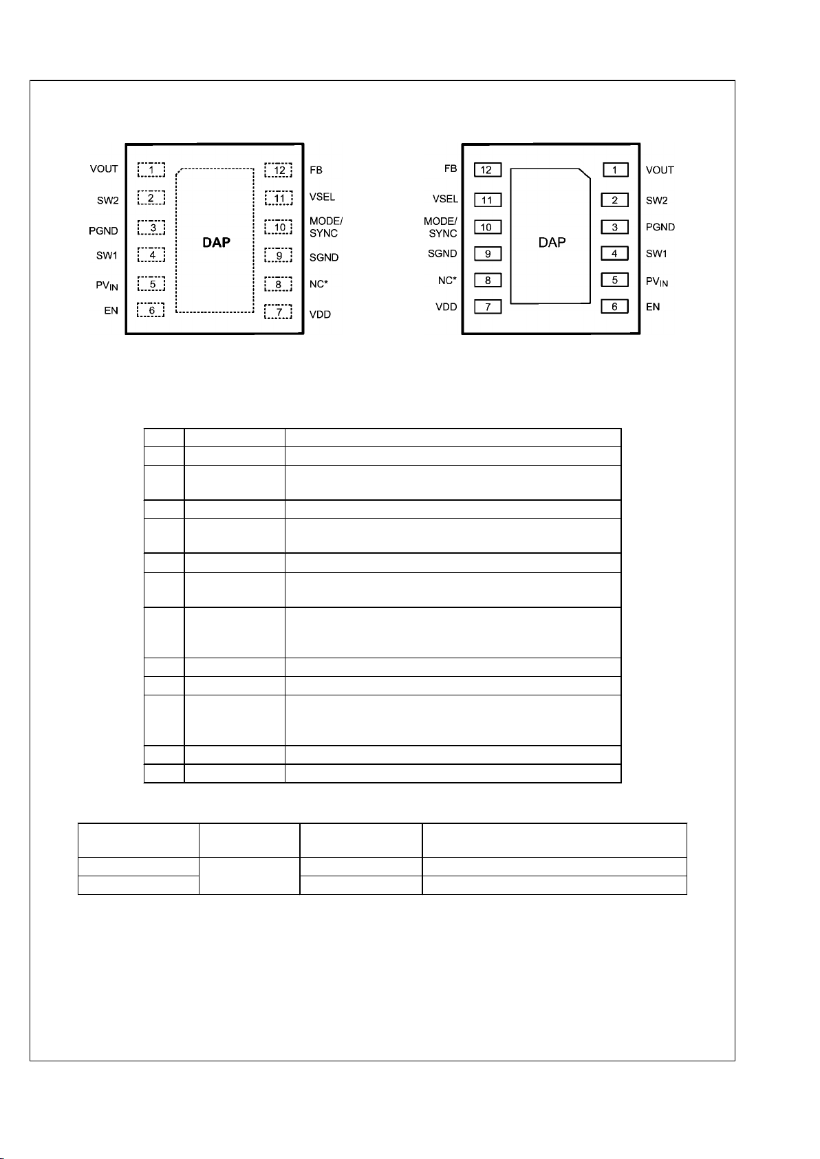
Connection Diagrams and Package Mark Information
20191402
Top View
20191403
Bottom View
Pin Descriptions
Pin # Pin Name Description
1 VOUT Connect to output capacitor.
2 SW2 Switching Node connection to the internal PFET switch (P2) and
NFET synchronous rectifier (N2).
3 PGND Power Ground.
4 SW1 Switching Node connection to the internal PFET switch (P1) and
NFET synchronous rectifier (N1).
5 PV
IN
Supply to the power switch, connect to the input capacitor.
6 EN Enable Input. Set this digital input high for normal operation. For
shutdown, set low.
7 VDD Signal Supply input. If board layout is not optimum an optional
1µF ceramic capacitor is suggested as close to this pin as
possible.
8 NC* No connect. Connect this pin to GND on PCB layout.
9 SGND Analog and Control Ground.
10 MODE/SYNC Mode = LOW, Automatic Mode. Mode= HI, Forced PWM Mode
SYNC = external clock synchronization from 1.6MHz to 2.7MHz
(When SYNC function is used, device is forced in PWM mode).
11 VSEL Logic input low = 2.8V and logic high = 3.3V to set output Voltage.
12 FB Feedback Analog Input. Connect to the output at the output filter.
Ordering Information
Order Number Package
NSC Package
Marking
Supplied As
LM3668SD - 3.3
LLP-12
S016B 1000 units, Tape and Reel
LM3668SDX - 3.3 S016B 4500 units, Tape and Reel
3 www.national.com
LM3668
Page 4
Absolute Maximum Ratings (Note 1)
If Military/Aerospace specified devices are required,
please contact the National Semiconductor Sales Office/
Distributors for availability and specifications.
PV
IN, VDD
Pin, SW1, SW2 & V
OUT
:
Voltage to SGND & PGND
−0.2V to +6.0V
FB, EN,MODE,SYNC pin: (PGND &
SGND-0.2V) to
(PVIN + 0.2)
PGND to SGND -0.2V to 0.2V
Continuous Power Dissipation
(Note 3)
Internally Limited
Maximum Junction Temperature
(T
J-MAX
)
+125°C
Storage Temperature Range −65°C to +150°C
Maximum Lead Temperature
(Soldering, 10 sec)
+260°C
Operating Ratings
Input Voltage Range 2.5V to 5.5V
Recommended Load Current 0mA to 1A
Junction Temperature (TJ) Range −40°C to +125°C
Ambient Temperature (TA) Range
(Note 3)
−40°C to +85°C
Thermal Properties
Junction-to-Ambient Thermal Resistance (θJA),
34°C/W
Leadless Lead frame Package (Note 5)
Electrical Characteristics (Notes 6, 7) Limits in standard typeface are for T
J
= +25°C. Limits in boldface type
apply over the full operating ambient temperature range (−40°C ≤ = TA ≤ +85°C). Unless otherwise noted: specifications apply to
the LM3668. VIN = 3.6V = EN, V
OUT
= 3.3V, CIN = 10 µF & C
OUT
= 22µF (Note 8).
Symbol Parameter Conditions Min Typ Max Units
V
FB
Feedback Voltage (Note 7)
-3 3 %
I
LIM
Switch Peak Current Limit Open loop(Note 2)
1.6 1.85 2.05 A
I
SHDN
Shutdown Supply Current EN =0V
0.01
1
µA
I
Q_PFM
DC Bias Current in PFM No load, device is not switching
(FB Forced higher than
programmed output voltage)
45 60 µA
I
Q_PWM
DC Bias Current in PWM PWM Mode, No Switching
600 750 µA
R
DSON(P)
Pin-Pin Resistance for PFET Switches P1 and P2
130 180
mΩ
R
DSON(N)
Pin-Pin Resistance for NFET Switches N1 and N2
100 150
mΩ
F
OSC
Internal Oscillator Frequency PWM Mode
1.9 2.2 2.5 MHz
F
SYNC
Sync Frequency Range VIN = 3.6V
1.6 2.7 MHz
V
IH
Logic High Input for EN, MODE/
SYNC pins
1.1 V
V
IL
Logic Low Input for EN, MODES/
SYNC pins
0.4 V
I
EN, MODE, SYNC
EN,MODES/SYNC pin Input Current
0.3 1 µA
Note 1: Absolute Maximum Ratings indicate limits beyond which damage to the component may occur. Operating Ratings are conditions under which operation
of the device is guaranteed. Operating Ratings do not imply guaranteed performance limits. For guaranteed performance limits and associated test conditions,
see the Electrical Characteristics tables.
Note 2: Electrical Characteristic table reflects open loop data (FB = 0V and current drawn from SW pin ramped up until cycle by cycle current limits is activated).
Closed loop current limit is the peak inductor current measured in the application circuit by increasing output current until output voltage drops by 10%.
Note 3: In applications where high power dissipation and/or poor package thermal resistance is present, the maximum ambient temperature may have to be
derated. Maximum ambient temperature (T
A-MAX
) is dependent on the maximum operating junction temperature (T
J-MAX-OP
= 125ºC), the maximum power
dissipation of the device in the application (P
D-MAX
), and the junction-to ambient thermal resistance of the part/package in the application (θJA), as given by the
following equation: T
A-MAX
= T
J-MAX-OP
– (θJA × P
D-MAX
).
Note 4: The Human body model is a 100 pF capacitor discharged through a 1.5 kΩ resistor into each pin. The machine model is a 200 pF capacitor discharged
directly into each pin. MIL-STD-883 3015.7
Note 5: Junction-to-ambient thermal resistance (θJA) is taken from a thermal modeling result, performed under the conditions and guidelines set forth in the
JEDEC standard JESD51-7. The test board is a 4-layer FR-4 board measuring 101.6mm x 76.2mm x 1.6mm. Thickness of the copper layers are 2oz/1oz/1oz/
2oz. The middle layer of the board is 60mm x 60mm. Ambient temperature in simulation is 22°C, still air.
Junction-to-ambient thermal resistance is highly application and board-layout dependent. In applications where high maximum power dissipation exists, special
care must be paid to thermal dissipation issues in board design.
Note 6: All voltage is with respect to SGND.
Note 7: Min and Max limits are guaranteed by design, test, or statistical analysis. Typical numbers are not guaranteed, but do represent the most likely norm.
Note 8: CIN and C
OUT
: Low-ESR Surface-Mount Ceramic Capacitors (MLCCs) used in setting electrical characteristics.
www.national.com 4
LM3668
Page 5
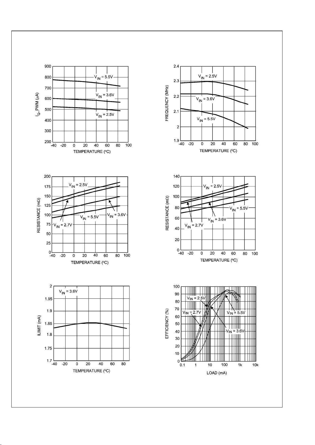
Typical Performance Characteristics Typical Application circuit Figure 1, V
IN
= 3.6V, L = 2.2µH, CIN =
10µF, C
OUT
= 22µF , TA = 25°C , Unless otherwise Stated.
Supply Current vs. Temperature ( Not switching)
20191439
Switching Frequency vs. Temperature
20191438
P_FET R
DS(ON)
vs. Temperature
20191442
N_FET R
DS(ON)
vs. Temperature
20191441
ILimit vs. Temperature
20191437
Efficiency at V
OUT
= 2.8V ( Forced PWM Mode)
20191427
5 www.national.com
LM3668
Page 6

Efficiency at V
OUT
= 2.8V ( Auto Mode)
20191428
Efficiency at V
OUT
= 3.3V ( Forced PWM Mode)
20191426
Efficiency V
OUT
= 3.3V ( Auto Mode)
20191425
Line Transient in Buck Mode
( V
OUT
= 3.3V, Load = 500mA)
20191431
Line Transient in Boost Mode
( V
OUT
= 3.3V, Load = 500mA)
20191432
Line Transient in Buck or Boost Mode
( V
OUT
= 3.3V, Load = 500mA)
20191433
www.national.com 6
LM3668
Page 7

Load Transient in Buck Mode ( PWM Mode)
VIN = 4.2V, V
OUT
= 3.3V, Load = 0-500mA
20191420
Load Transient in Boost Operation ( PWM Mode)
VIN = 2.7V, V
OUT
= 3.3V, Load = 0-500mA
20191422
Load Transient in Buck-Boost Operation ( PWM Mode)
V
IN
= 3.4V, V
OUT
= 3.3V, Load = 0-500mA
20191421
Load Transient in Boost Operation (Auto Mode)
VIN = 2.7V, V
OUT
= 3.3V, Load = 50-150mA
20191434
Load Transient in Buck Operation ( Auto Mode)
VIN = 4.2V, V
OUT
= 3.3V, Load = 50-150mA
20191436
Load Transient in Buck - Boost Mode ( Auto Mode)
VIN = 3.6V, V
OUT
= 3.3V, Load = 50-150mA
20191435
7 www.national.com
LM3668
Page 8

Typical PWM Switching Waveform ( Boost operation)
VIN = 3V, V
OUT
= 3.3V, Load = 500mA
20191416
Typical PWM Switching Waveform ( Buck operation)
VIN = 4V, V
OUT
= 3.3V, Load = 500mA
20191417
Typical PFM Switching Waveform ( Buck operation)
VIN = 4V, V
OUT
= 3.3V,Load = 50mA
20191418
Typical PFM Switching Waveform ( Boost operation)
VIN = 3V, V
OUT
= 3.3V, Load = 50mA
20191419
Start up in PWM Mode
20191429
Start up in PWM Mode
20191430
www.national.com 8
LM3668
Page 9

Circuit Description
The LM3668, a high efficiency Buck or Boost DC-DC converter, delivers a constant voltage from either a single Li-Ion
or three cell NIMH/NiCd battery to portable devices such as
mobiles phone and PDAs. Using a voltage mode architectures with synchronous rectification, the LM3668 has the
ability to deliver up to 1A depending on the input voltage, output voltage, ambient temperature and the chosen inductor.
In addition, the device incorporates a seamless transition
from buck to boost or boost to buck mode. The internal error
amplifier continuously monitors the output to determine the
transition from buck to boost or boost to buck operation. Fig-
ure 2 shows the four switches network used for the buck and
boost operation. Table 1 summarizes the state of the swtiches
in different Modes.
There are three modes of operation depending on the current
required: PWM (Pulse Width Modulation), PFM (Pulse Frequency Modulation), and shutdown. The device operates in
PWM mode at load currents of approximately 80mA or higher
to improve efficiency. Lighter load current causes the device
to automatically switch into PFM mode to reduce current consumption and extend battery life. Shutdown mode turns off
the device, offering the lowest current consumption.
20191405
FIGURE 2. Simplified Diagram of Switches
State of Switches in Different Modes
Mode Always ON Always
OFF
Switching
Buck SW P2 SW N2 SW P1 & N1
Boost SW P1 SW N1 SW N2 & P2
TABLE 1
Buck Operation
When the input voltage is greater than the output voltage, the
device operates in buck mode where switch P2 is always ON
and P1 & N1 control the output . Figure 4 shows the simplified
circuit for buck mode operation.
20191406
FIGURE 3. Simplified Circuit for Buck Operation
Boost Operation
When the input voltage is smaller than the output voltage, the
device enters boost mode operation where P1 is always ON,
while Switches N2 & P2 control the output. Figure 5 shows
the simplified circuit for boost mode operation.
20191408
FIGURE 4. Simplified Circuit for Boost Operation
PWM Operation
In PWM operation, the output voltage is regulated by switching at a constant frequency and then modulating the energy
per cycle to control power to the load. In Normal operation,
the internal error amplifier provides an error signal, Vc, from
the feedback voltage and Vref. The error amplifier signal, Vc,
is compared with a voltage, Vcenter, and used to generate
the PWM signals for both Buck & Boost Modes. Signal Vcenter is a DC signal which sets the transition point of the buck
and boost modes. Below are three regions of operation:
•
Region I, If Vc is less than Vcenter, Buck mode.
•
Region II, If Vc and Vcenter are equal, both PMOS
switches (P1, P2) are on and both NMOS switches (N1,
N2) are off. The power passes directly from input to output
via P1 & P2
•
Region III, If Vc is greater than Vcenter, Boost Mode.
The Buck-boost operation is avoided, to improve the efficiency across VIN and load range.
20191415
FIGURE 5. PWM Generator Block Diagram
9 www.national.com
LM3668
Page 10

Internal Synchronous Rectification
While in PWM mode, the LM3668 uses an internal MOSFET
as a synchronous rectifier to reduce rectifier forward voltage
drop and associated power loss. Synchronous rectification
provides a significant improvement in efficiency whenever the
output voltage is relatively low compare to the voltage drop
across an ordinary rectifier diode.
PFM Operation
At very light loads, the converter enters PFM mode and operates with reduced switching frequency and supply current
to maintain high efficiency. The part automatically transitions
into PFM mode when either of two following conditions occur
for a duration of 128 or more clock cycles:
A. The inductor current reaches zero.
B. The peak inductor current drops below the I
MODE
level,
(Typically I
MODE
< 45mA + VIN/80 Ω ).
In PFM operation, the compensation circuit in the error amplifier is turned off. The error amplifier works as a hysteretic
comparator. The PFM comparator senses the output voltage
via the feedback pin and controls the switching of the output
FETs such that the output voltage ramps between ~0.8% and
~1.6% of the nominal PWM output voltage (Figure 6). If the
output voltage is below the ‘high’ PFM comparator threshold,
the P1 & P2 (Buck mode) or N2 & P1 (Boost mode) power
switches are turned on. It remains on until the output voltage
reaches the ‘high’ PFM threshold or the peak current exceeds
the I
PFM
level set for PFM mode. The typical peak current in
PFM mode is: I
PFM
= 220mA
Once the P1 ( Buck mode) or N2 ( Boost mode) power switch
is turned off, the N1 & P2 ( Buck mode) or P1 & P2 (Boost
mode) power switches are turned on until the inductor current
ramps to zero. When the zero inductor current condition is
detected, the N1( Buck mode) or P2 ( Boost mode) power
switches are turned off. If the output voltage is below the ‘high’
PFM comparator threshold, the P1 & P2 (Buck mode) or N2
& P1 ( Boost mode) switches are again turned on and the
cycle is repeated until the output reaches the desired level.
Once the output reaches the ‘high’ PFM threshold, the N1 &
P2 (Buck mode) or P1 & P2 ( Boost mode) switches are turned
on briefly to ramp the inductor current to zero and then both
output switches are turned off and the part enters an extremely low power mode. Quiescent supply current during this
‘sleep’ mode is 45µA (typ), which allows the part to achieve
high efficiency under extremely light load conditions.
20191413
FIGURE 6. PFM to PWM Mode Transition
In addition to the auto mode transition, the LM3668 operates
in PFM Buck or PFM Boost based on the following conditions.
There is a small delta (~500mV) known as dv1(~200mV) &
dv2(~300mV) when V
OUT_TARGET
is very close to V
IN
where
the LM3668 can be in either buck or boost mode. For example
when V
OUT_TARGET
= 3.3V and VIN is between 3.1V & 3.6V,
the LM3668 can be in either mode depending on the VIN vs
V
OUT_TARGET
.
•
Region I: If VIN < V
OUT_TARGET
- dv1, the regulator operates
in boost mode.
•
Region II: If V
OUT_TARGET
- dv1 < VIN < V
OUT_TARGET
+
dv2 ,the regulator operates in either buck or boost mode.
•
Region III: If VIN > V
OUT_TARGET
+ dv2, the regulator
operates in buck mode.
20191414
FIGURE 7. V
OUT
vs VIN Transition
www.national.com 10
LM3668
Page 11

In the buck PFM operation, P2 is always turned on and N2 is
always turned off , P1 and N1 power switches are switching.
P1 and N1 are turned off to enter " sleep mode" when the
output voltage reaches the "high" comparator threshold. In
boost PFM operation, P2 and N2 are switching. P1 is turned
on and N1 is turned off when the output voltage is below the
"high" threshold. Unlike in buck mode, all four power switches
are turned off to enter "sleep" mode when the output voltage
reaches the "high" threshold in boost mode. In addition, the
internal current sensing of the I
PFM
is used to determine the
precise condition to switch over to buck or boost mode via the
PFM generator.
Current Limit Protection
The LM3668 has current limit protection to prevent excessive
stress on itself and external components during overload conditions. The internal current limit comparator will disable the
power device at a typical switch peak current limit of 1.85A
(typ.).
Under Voltage Protection
The LM3668 has an UVP comparator to turn the power device
off in case the input voltage or battery voltage is too low . The
typical UVP threshold is around 2V.
Short Circuit Protection
When the output of the LM3668 is shorted to GND, the current
limit is reduced to about half of the typical current limit value
until the short is removed.
Thermal Shutdown
The LM3668 has an internal thermal shutdown function to
protect the die from excessive temperatures. The thermal
shutdown trip point is typically 150°C, Normal operation resumes when the temperature drops below 125°C.
Start-up
The LM3668 has a soft-start circuit that smooth the output
voltage and ramp current during start-up. During start-up the
bandgap reference is slowly ramped up and switch current
limit is reduced to half the typical value. Soft start is activated
only if EN goes from logic low to logic high after Vin reaches
2.5V. The start-up time thereby depends on the output capacitor and load current demanded at start-up. It is not recommended to start up the device at full load while in softstart.
Application Information
SYNC/MODE PIN
If the SYNC/MODE pin is set high, the device is set to operate
at PWM mode only. If SYNC/MODE pin is set low, the device
is set to automatically transition from PFM to PWM or PWM
to PFM depending on the load current. Do not leave this pin
floating. The SYNC/MODE pin can also be driven by an external clock to set the desired switching frequency between
1.6MHz to 2.7MHz.
V
SEL
Pin
The LM3668 has built in logic for conveniently setting the output voltage, with V
SEL
high, the output is set to 3.3V; with
V
SEL
low the output is set to 2.8V. It is not recommended to
use this function for dynamically switching between 2.8V and
3.3V.
Maximum Current
The LM3668 is designed to operate up to 1A. For input voltages at 2.5V, the maximum operating current is 600mA and
800mA for 2.7V input voltage. In any mode it is recommended
to avoid starting up the device at minmum input voltage and
maximum load. Special attention must be taken to avoid operating near thermal shutdown when operating in boost mode
at maximum load (1A). A simple calculation can be used to
determine the power dissipation at the operating condition;
P
D-MAX
= (T
J-MAX-OP
– T
A-MAX
)/θJA . The LM3668 has thermal
resistance θ
JA
= 34°C/W ((Note 3) and (Note 5)), and maximum operating ambient of 85°C. As a result, the maximum
power dissipation using the above formula is around
1176mW. Refer to dissipation table below for P
D-MAX
value at
different ambient temperatures.
Dissipation Rating Table
θ
JA
TA ≤ 25°C TA ≤ 60°C TA ≤ 85°C
34°C/W ( 4
layers board
per JEDEC
standard)
2941mW 1912mW 1176mW
Inductor Selection
There are two main considerations when choosing an inductor; the inductor should not saturate, and the inductor current
ripple should be small enough to achieve the desired output
voltage ripple. Different saturation current rating specifications are followed by different manufacturers so attention
must be given to details. Saturation current ratings are typically specified at 25°C. However, ratings at the maximum
ambient temperature of application should be requested from
the manufacturer. Shielded inductors radiate less noise and
should be preferred.
In the case of the LM3668, there are two modes ( Buck &
Boost) of operation that must be consider when selecting an
inductor with appropriate saturation current. The saturation
current should be greater than the sum of the maximum load
current and the worst case average to peak inductor current.
The first equation shows the buck mode operation for worst
case conditions and the second equation for boost condition.
•
I
RIPPLE
: peak inductor current
•
I
OUTMAX
: maximum load current
•
VIN: maximum input voltage in application
11 www.national.com
LM3668
Page 12

•
L : min inductor value including worst case tolerances
(30% drop can be considered)
•
f : minimum switching frequency
•
V
OUT
: output voltage
•
D: Duty Cycle for CCM Operation
•
V
OUT
: Output Voltage
•
VIN: Input Voltage
Example using above equations:
•
VIN = 2.8V to 4V
•
V
OUT
= 3.3V
•
I
OUT
= 500mA
•
L = 2.2µH
•
F = 2MHz
•
Buck: I
SAT
= 567mA
•
Boost: I
SAT
= 638mA
As a result the inductor should be selected according to the
highest of the two I
SAT
values.
A more conservative and recommended approach is to
choose an inductor that has a saturation current rating greater
than the maximum current limit of 2.05A.
A 2.2 µH inductor with a saturation current rating of at least
2.05A is recommended for most applications.The inductor’s
resistance should be less than 100mΩ for good efficiency. For
low-cost applications, an unshielded bobbin inductor could be
considered. For noise critical applications, a toroidal or shielded-bobbin inductor should be used. A good practice is to lay
out the board with overlapping footprints of both types for design flexibility. This allows substitution of a low-noise shielded
inductor, in the event that noise from low-cost bobbin model
is unacceptable.
Suggest Inductors and Suppliers
Model Vendor Dimension
s
LxWxH
(mm)
D.C.R
(max)
I
SAT
LPS4012-
222L
Coilcraft 4 x 4 x 1.2
100 mΩ
2.1A
LPS4018-
222L
Coilcraft 4 x 4 x 1.8
70 mΩ
2.5A
1098AS-2
R0M (2µF)
TOKO 3 x 2.8x 1.2
67 mΩ
1.8A
( lower
current
application
s)
Input Capacitor Selection
A ceramic input capacitor of at least 10 µF, 6.3V is sufficient
for most applications. Place the input capacitor as close as
possible to the PVIN pin of the device. A larger value may be
used for improved input voltage filtering. Use X7R or X5R
types; do not use Y5V. DC bias characteristics of ceramic capacitors must be considered when selecting case sizes like
0805 or 0603. The input filter capacitor supplies current to
the PFET switch of the LM3668 in the first half of each cycle
and reduces voltage ripple imposed on the input power
source. A ceramic capacitor’s low ESR provides the best
noise filtering of the input voltage spikes due to this rapidly
changing current.
Output Capacitor Selection
A ceramic output capacitor of 22µF, 6.3V is sufficient for most
applications. Multilayer ceramic capacitors such as X5R or
X7R with low ESR is a good choice for this as well. These
capacitors provide an ideal balance between small size, cost,
reliability and performance. Do not use Y5V ceramic capacitors as they have poor dielectric performance over temperature and poor voltage characteristic for a given value.
Extra attention is required if a smaller case size capacitor is
used in the application. Smaller case size capacitors typically
have less capacitance for a given bias voltage as compared
to a larger case size capacitor with the same bias voltage.
Please contact the capacitor manufacturer for detail information regarding capacitance verses case size. Table 1 lists
several capacitor suppliers.
The output filter capacitor smoothes out current flow from the
inductor to the load, helps maintain a steady output voltage
during transient load changes and reduces output voltage
ripple. These capacitors must be selected with sufficient capacitance and sufficiently low ESR to perform these functions.
Note that the output voltage ripple is dependent on the inductor current ripple and the equivalent series resistance of the
output capacitor (R
ESR
).
The R
ESR
is frequency dependent (as well as temperature
dependent); make sure the value used for calculations is at
the switching frequency of the part.
TABLE 1. Suggested Capacitors and Suppliers
Model Type Vendor Voltage Rating
Case Size
Inch (mm)
10 µF for C
IN
GRM21BR60J106K Ceramic, X5R Murata 6.3V 0805 (2012)
JMK212BJ106K Ceramic, X5R Taiyo-Yuden 6.3V 0805 (2012)
C2012X5R0J106K Ceramic, X5R TDK 6.3V 0805 (2012)
22 µF for C
OUT
JMK212BJ226MG Ceramic, X5R Taiyo-Yuden 6.3V 0805 (2012)
www.national.com 12
LM3668
Page 13

Layout Considerations
As for any high frequency switcher, it is important to place the
external components as close as possible to the IC to maximize device performance. Below are some layout recommendations:
1) Place input filter and output filter capacitors close to the IC
to minimize copper trace resistance which will directly effect
the overall ripple voltage.
2) Route noise sensitive trace away from noisy power components. Separate power GND ( Noisy GND) and Signal GND
( quiet GND) and star GND them at a single point on the PCB
prefereably close to the device GND pin.
3) Connect the ground pins and filter capacitors together via
a ground plane to prevent switching current circulating
through the ground plane. Additional layout consideration regarding the LLP package can be found in Application AN1187
13 www.national.com
LM3668
Page 14

Physical Dimensions inches (millimeters) unless otherwise noted
12–Pin LLP
NS Package Number SDF12A
www.national.com 14
LM3668
Page 15

Notes
15 www.national.com
LM3668
Page 16

Notes
LM3668 1A, High Efficiency Dual Mode Single Inductor Buck-Boost DC/DC Converter
THE CONTENTS OF THIS DOCUMENT ARE PROVIDED IN CONNECTION WITH NATIONAL SEMICONDUCTOR CORPORATION
(“NATIONAL”) PRODUCTS. NATIONAL MAKES NO REPRESENTATIONS OR WARRANTIES WITH RESPECT TO THE ACCURACY
OR COMPLETENESS OF THE CONTENTS OF THIS PUBLICATION AND RESERVES THE RIGHT TO MAKE CHANGES TO
SPECIFICATIONS AND PRODUCT DESCRIPTIONS AT ANY TIME WITHOUT NOTICE. NO LICENSE, WHETHER EXPRESS,
IMPLIED, ARISING BY ESTOPPEL OR OTHERWISE, TO ANY INTELLECTUAL PROPERTY RIGHTS IS GRANTED BY THIS
DOCUMENT.
TESTING AND OTHER QUALITY CONTROLS ARE USED TO THE EXTENT NATIONAL DEEMS NECESSARY TO SUPPORT
NATIONAL’S PRODUCT WARRANTY. EXCEPT WHERE MANDATED BY GOVERNMENT REQUIREMENTS, TESTING OF ALL
PARAMETERS OF EACH PRODUCT IS NOT NECESSARILY PERFORMED. NATIONAL ASSUMES NO LIABILITY FOR
APPLICATIONS ASSISTANCE OR BUYER PRODUCT DESIGN. BUYERS ARE RESPONSIBLE FOR THEIR PRODUCTS AND
APPLICATIONS USING NATIONAL COMPONENTS. PRIOR TO USING OR DISTRIBUTING ANY PRODUCTS THAT INCLUDE
NATIONAL COMPONENTS, BUYERS SHOULD PROVIDE ADEQUATE DESIGN, TESTING AND OPERATING SAFEGUARDS.
EXCEPT AS PROVIDED IN NATIONAL’S TERMS AND CONDITIONS OF SALE FOR SUCH PRODUCTS, NATIONAL ASSUMES NO
LIABILITY WHATSOEVER, AND NATIONAL DISCLAIMS ANY EXPRESS OR IMPLIED WARRANTY RELATING TO THE SALE
AND/OR USE OF NATIONAL PRODUCTS INCLUDING LIABILITY OR WARRANTIES RELATING TO FITNESS FOR A PARTICULAR
PURPOSE, MERCHANTABILITY, OR INFRINGEMENT OF ANY PATENT, COPYRIGHT OR OTHER INTELLECTUAL PROPERTY
RIGHT.
LIFE SUPPORT POLICY
NATIONAL’S PRODUCTS ARE NOT AUTHORIZED FOR USE AS CRITICAL COMPONENTS IN LIFE SUPPORT DEVICES OR
SYSTEMS WITHOUT THE EXPRESS PRIOR WRITTEN APPROVAL OF THE CHIEF EXECUTIVE OFFICER AND GENERAL
COUNSEL OF NATIONAL SEMICONDUCTOR CORPORATION. As used herein:
Life support devices or systems are devices which (a) are intended for surgical implant into the body, or (b) support or sustain life and
whose failure to perform when properly used in accordance with instructions for use provided in the labeling can be reasonably expected
to result in a significant injury to the user. A critical component is any component in a life support device or system whose failure to perform
can be reasonably expected to cause the failure of the life support device or system or to affect its safety or effectiveness.
National Semiconductor and the National Semiconductor logo are registered trademarks of National Semiconductor Corporation. All other
brand or product names may be trademarks or registered trademarks of their respective holders.
Copyright© 2007 National Semiconductor Corporation
For the most current product information visit us at www.national.com
National Semiconductor
Americas Customer
Support Center
Email:
new.feedback@nsc.com
Tel: 1-800-272-9959
National Semiconductor Europe
Customer Support Center
Fax: +49 (0) 180-530-85-86
Email: europe.support@nsc.com
Deutsch Tel: +49 (0) 69 9508 6208
English Tel: +49 (0) 870 24 0 2171
Français Tel: +33 (0) 1 41 91 8790
National Semiconductor Asia
Pacific Customer Support Center
Email: ap.support@nsc.com
National Semiconductor Japan
Customer Support Center
Fax: 81-3-5639-7507
Email: jpn.feedback@nsc.com
Tel: 81-3-5639-7560
www.national.com
 Loading...