

Page 1
LM3647 Universal Battery Charger for Li-Ion, Ni-MH and Ni-Cd Batteries
©2000 National Semiconductor Corporation www.national.com
LM3647
Universal Battery Charger
for Li-Ion, Ni-MH and Ni-Cd Batteries
1.0 General Description
The LM3647 is a charge controller for Lithium-Ion (Li-Ion),
Nickel-Metal Hydride (Ni-MH) and Nickel-Cadmium (NiCd) batteries. The device can use either a pulsed-current
charging or a constant-current charging technique. The
device can also be configured to discharge before charging. Throughout the charging sequence the LM3647 monitors voltage and/or temperature and time in order to
terminate charging.
■ Negative delta voltage (-∆V)
■ Maximum voltage
■ Optional: Delta temperature/delta time (∆T/∆t)
■ Optional: Maximum temperature
■ Backup: Maximum time
If both voltage and temperature fail to trigger the termination requirements, then the maximum time (configured by
externalhardware)stepsinwhichterminates the charging.
In Ni-Cd/Ni-MH mode, four different charging stages are
used:
■ Soft-start charge
■ Fast charge
■ Topping charge
■ Maintenance charge
In Li-Ion mode, four different charging stages are used:
■ Qualification
■ Fast Charge Phase 1, Constant Current
■ Fast Charge phase 2, Constant Voltage
■ Maintenance charge
The charge current of the LM3647 is configured via external resistors, which in turn controls the duty cycle of the
PWM switching control output. For cost-sensitive applications, the LM3647 charge controller can be configured
without a temperature sensor and to use an external current source.
PRELIMINARY
March 2000
When using an external current source, the current is controlled by the LM3647 which turns the current source on
and off. The LM3647 automatically detects the presence of
a battery and starts the charging procedure when the battery is installed. Whenever an error occurs (e.g., short circuit, temperature too high, temperature too low, bad
battery,chargetime over,etc.) the LM3647 will stay in error
mode until the battery is removed or it gets within the allowed charging temperature range. The LM3647 is available in a standard 20-lead SOIC surface mount package.
Key Features
■ Auto-adaptive fast charge
■ High-resolution, accurate voltage monitoring prevents
Li-Ion undercharge or overcharge
■ Fast charge, pre-charge and maintenance currents are
provided. Different currents are selectable via external
resistors.
■ Fast-charge termination by ∆ temperature/∆ time, maxi-
mum voltage, maximum temperature, negative ∆ voltage and maximum time
■ Dynamically detects battery insertion, removal, short
circuit and bad battery without additional hardware
■ Supports charging of battery packs with 2-8 cells of NiCd/Ni-MH or 1-4 cells of Li-Ion
■ Three LED indicators and Buzzer output indicate operational modes
■ Ni-MH/Ni-Cd charge mode, Li-Ion charge mode or discharge mode can be selected manually
■ PWM switching controller
Applications
■ Battery charging systems for:
— Portable consumer electronics
— Audio/video equipment
— Communications equipment
— Point of sale devices
— Power tools
— Personal convenience products
Page 2
2 www.national.com
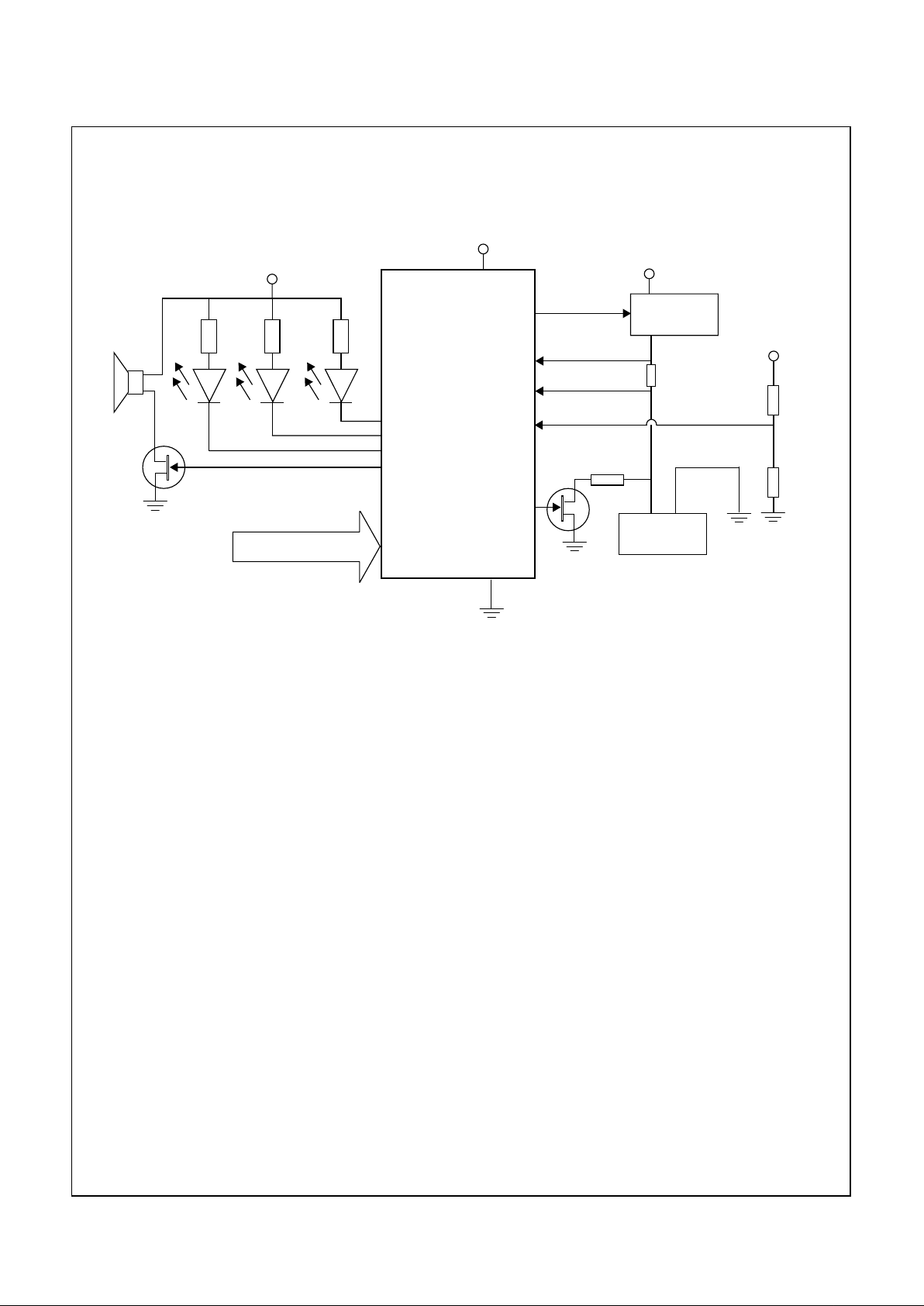
Typical Application
RCIN
SEL1 ... SEL4
DISCHG
PMW
CS
CEL
TEMP
LED1
LED2
LED3
BUZZER
LM3647
BATTERY
CONTROL
CURRENT
VOLT AGE
TEMPERATURE
POWER
UNREGULATED
DC VOLTAGE (MAX 20V)
CONFIGURATIONS
Vcc
Vcc
Vcc
NTC
Current
Source
Resistor
Page 3
3 www.national.com
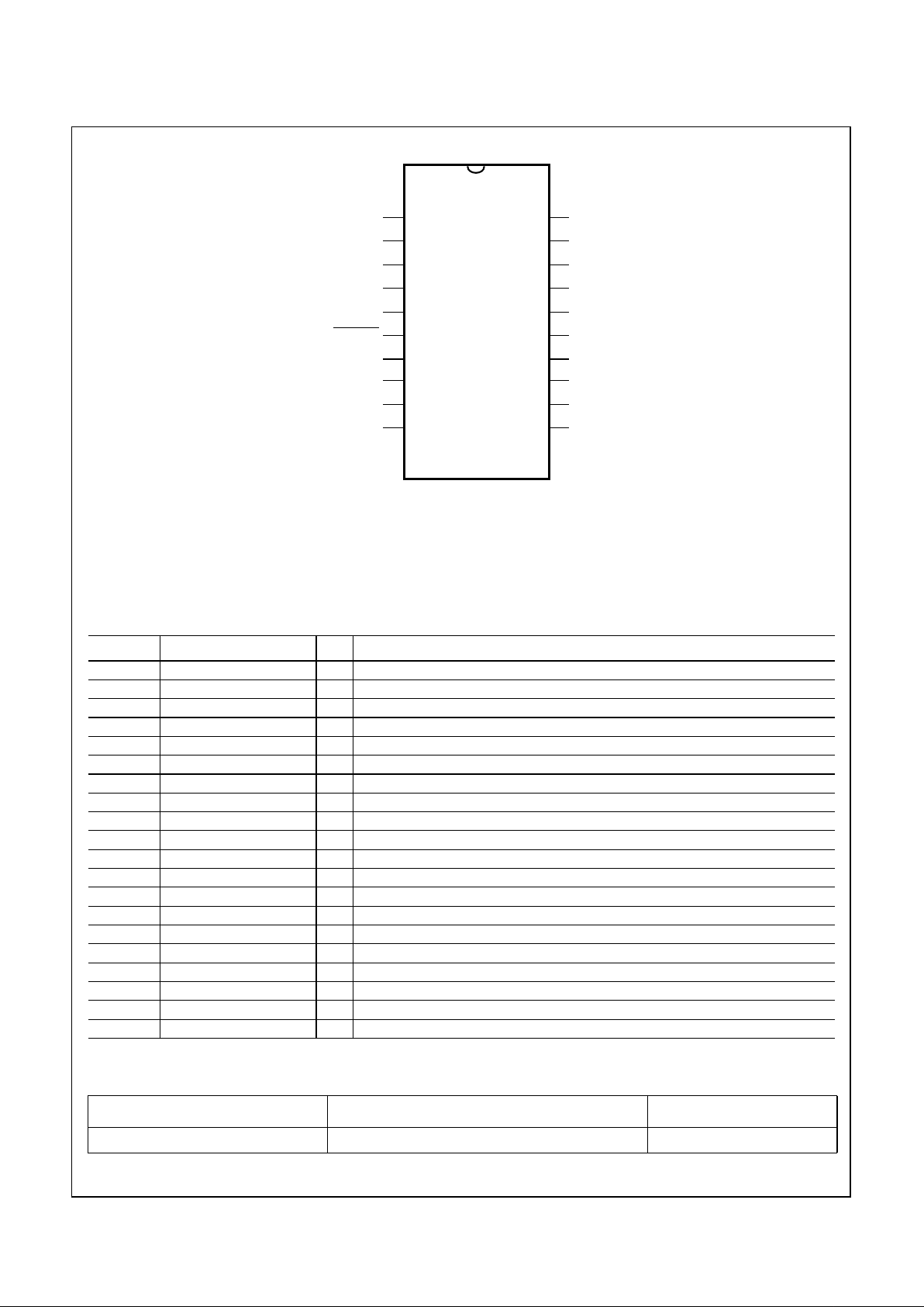
2. Connection Diagram
2.1 Pin Descriptions
2.2 Ordering Information
Pin No. Name I/O Description
1 SEL3 I Input to select charge mode: high = pulse, low = constant
2 SEL4 I Input to select maintenance time out, connected to an RC-network
3 RCIN RC-timing pin
4 GND Ground
5 Vcc 5V, power supply
6 RESET I Reset pin, active low
7 LED1 O LED output
8 LED2 O LED output
9 LED3 O LED output
10 VREF I Voltage reference analog input
11 CEXT External Capacitor
12 CEL I Battery voltage input (through resistor divider)
13 CS I Current sense input
14 TEMP I NTC-temperature sensor input
15 DISCHG O High when discharging, else low
16 SYSOK O System Monitor Output
17 BUZZER O Buzzer output
18 PWM O PWM-output filtered to a DC-level (controls the current)
19 SEL1 I Tri-level input, used to select charge type
20 SEL2 I Tri-level input, used to select NiCd, NiMH, Li-Ion
Device Package Temperature
LM3647IM 20 SOIC -40˚C to +85˚C
RESET
TEMP
CS
CEL
CEXT
BUZZER
DISCHG
SEL2
SEL1
PWM
20-PIN
SOIC
SEL3
SEL4
RCIN
GND
V
CC
LED1
LED2
LED3
Top View
1
2
3
4
5
6
7
8
9
10
20
19
18
17
16
15
14
13
12
11
V
REF
SYSOK
Order Number LM3647IM
NS Package Number M20B
Page 4
4 www.national.com
3.0 Electrical Characteristics
Absolute Maximum Ratings
Note: If Military/Aerospace specified devices are required
please contact the National Semiconductor Sales Office/Distributors for availability and specifications.
Note: Absolute maximum ratings indicate limits beyond
which damage to the device mayoccur.DC and AC electrical
specifications are not ensured when operating the device at
absolute maximum ratings.
DC Electrical Characteristics: -40˚C ≤ T
A
≤ +85˚C unless otherwise specified
AC Electrical Characteristics
Supply Voltage (VCC)7V
Voltage at Any Pin –0.3V to V
CC
+ 0.3V
Total Current into V
CC
Pin (Source) 100 mA
Total Current out of GND Pin (Sink) 110 mA
Storage Temperature Range –65˚C to +140˚C
Parameter Conditions Min Typ Max Units
Operating Voltage 4.5 5.5 V
Supply Current 2.5 mA
LED-pin Sink Current 7.5 15 mA
Temperature Input Levels
Ni-Cd / Ni-MH Upper limit (Voltage at TEMP-pin) 3.15 V
Li-Ion Upper limit (Voltage at TEMP-pin) 3.0 V
Lower Limit (Voltage at TEMP-pin) 0.5 V
Start limit (Voltage at TEMP-pin) 2.2 V
Li-Ion (for both 4.1 and 4.2V Cells)
Maintenance Charge Minimum Voltage (CEL pin) 2.6 V
Maintenance Charge Restart Voltage (CEL pin) 2.153 V
Good Battery Threshold (CEL pin) 1.2 V
Maintenance Current (Voltage at CS-pin) 2.3 V
Maintenance Current Lower Threshold (Voltage at CS-pin) 2.42 V
Minimum Current Fast Charge Termination (Voltage at CS-pin) 2.3 V
Qualification Current (Voltage at CS-pin) 2.3 V
Maximum Charging Current (Voltage at CS-pin) 1.5 V
Ni-Cd/Ni-MH
Maximum Battery Voltage (CEL pin) 3.017 V
Maximum Battery Current (Voltage at CS-pin) 1.5 V
Battery Presence Limit (CEL pin) 1.0 V
Discharged Battery Limit (CEL pin) 1.7 V
Good Battery Threshold (CEL pin) 1.2 V
Soft Start Current (Voltage at CS-pin) 2.3 V
Topping Charge Current (Voltage at CS-pin) 2.3 V
Maintenance Charge Current (Voltage at CS-pin) 2.425 2.45 V
V
REF
2.5 V
Parameter Conditions Min Typ Max Units
RCIN frequency R = 3.3kΩ, C = 68pF 2.5 MHz
Fast-PWM frequency 250 Hz
Slow-PWM frequency 0.1 Hz
Page 5
5 www.national.com
4.0 Functional Description
4.1 General
The LM3647 can be configured to charge three different
types of batteries: Ni-Cd, Ni-MH and Li-Ion. The charger behavior for Ni-Cd and Ni-MH is similar but the charge curves
will appear slightly different due to the differences in chemistry. The Ni-Cd/Ni-MH charging algorithm is divided into four
phases:
Soft Start: The LM3647 detects that a battery is connected
and verifies that the temperature is within limit.
Charging starts with a current of 0.2C and switches into next phase on timeout. Error termination
will be triggered by Maximum Battery Voltage
(CEL-pin > 3.017V) or if the battery voltage never
reaches the Defective Battery Level (CEL-pin <
1.2V).
Fast Charge: Constant current is applied to the battery and
the LM3647 monitors voltage and temperature
(optional). Switch into next phase will appear as a
voltage drop in the charging curve: (Ni-Cd ~
50mV/cell) and (Ni-MH ~ 17mV/cell). Error termination will be triggered by over-temperature.
Topping Charge: A current of 0.2C is applied to the battery
for a user defined time (RC network at SEL4)
Maintenance Charge: Is user selectable and is a fixed per-
centage of the Fast Charge rate.
Discharge before charge is user selectable.
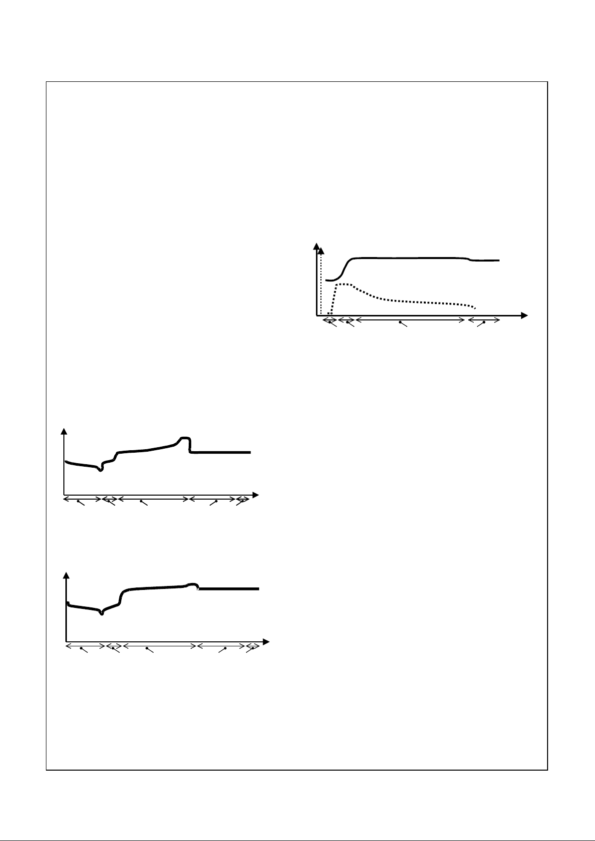
Ni-Cd Charging Curve:
Ni-MH Charging Curve:
The Li-Ion charging algorithm is also divided into four phases:
■ Qualification: The LM3647 detects that a battery is con-
nected and verifies that the temperature (optional but
highly recommended for safety reasons) is within limit.
Charging starts with a current of 0.2C and switches into
next phase on timeout (~ 1 minute). Error termination will
be triggered if the battery voltage does not reach the LiIon Battery Qualification Level (CEL-pin < 1.2V) within
one minute.
■ Fast Charge Constant Current: Battery voltage will rise
until Maximum Battery Voltage (CEL-pin = 2.675V or
2.74V depending on SEL3) is reached.
■ Fast Charge Constant Voltage: Keeps the voltage con-
stant until the current has decreased below the threshold
(CS at 2.3V).
■ Maintenance Charge: Is user selectable and is a fixed
percentage of the Fast Charge rate.
4.2 Advanced Pin Descriptions
SEL1 is a selection pin to set the LM3647 in different charge
behavior. The pin has three states: tied to Vcc, GND, or unconnected (Hi-Z). When the charger is configured to charge
Ni-Cd or Ni-MH batteries, this pin determines if the charger
discharges the battery before charging or if the charger shall
only maintenance charge the battery. When the charger is
configured for Li-Ion batteries, this pin determines how the
charger behaves during maintenance charge.
SEL2 is a selection pin to determine the battery type to be
charged. The pin has three states: tied to Vcc (Ni-MH), GND
(Ni-Cd), or unconnected (Li-lon).
SEL3 is a selection pin used to set charger hardware modes.
The pin has two states: tied to Vcc or GND. When configured
for Ni-Cd/Ni-MH batteries, this pin determines whether the
PWM is fast and has current feedback, or slow and has external current control. When configured for Li-Ion batteries,
this pin changes the regulation point for maximum voltage,
2.675V (4.1V Cell) or 2.74V (4.2V Cell).
Note: SEL3 must be hard wired to Vcc if a charger that supports both Li-Ion and Ni-Cd Ni-MH is implemented.
SEL4 is connected to a RC-network that determines the
charge time-outs. This RC-network is also connected to the
output LED1.
RCIN is a high-speed timing pin, used to drive the charger at
the right frequency connected to a RC-network.
GND is the ground pin.
Vcc is the power-supply pin. This pin should have a 100nF
capacitor tied to GND.
RESET is a reset pin.
LED1 is an active-low output used to indicate charge phase.
It is also used when measuring the charge timeout value.
Voltage
Time
Discharge Soft Start Fast Charge
Topping
Charge
Maintenance
Charge
Voltage
Time
Discharge Soft Start Fast Charge
Topping
Charge
Maintenance
Charge
Voltage
Time
Qualification
Fast Charge
Constant Current
Fast Charge
Constant Voltage
Maintenance
Charge
Current
Page 6
6 www.national.com
LED2 is an active-low output used to indicate charge or discharge. It also sends out digitally what the LM3647 has read
at the mode selection pins and charge timeout.
LED3 is an active-low output used to indicate charge start/
stop and error.
VREF is the voltage reference analog input. The LM3647
uses this pin as a reference when measuring the other analog inputs.
CEXT is a timing pin used by the LM3647, it must be connected to a low loss capacitor.
CEL is an analog input that measures the battery voltage via
a resistor divider network.
CS is an analog input that is connected to a differential amplifier that measures the voltage overa small current sensing
resistor.
TEMP is an analog input thatis connected to the temperature
sensing NTC-resistor (if used). If no temperature sensor is
used, the input must be biased to approximate 1.5-2V.
DISCHG is a digital output that controls a power-FET that
dischargesthe batteries before charging them. If thisfunction
is not used then leave this pin unconnected.
SYSOK is an open drain output that resets the LM3647 in the
rare case of an internal illegal operating condition. This pin is
connected to the RESET pin to increase reliable operation of
the device in hostile operating environments (e.g., noisy environments).
BUZZER is a digital output that controls a small FET and
turns the buzzer on and off. The buzzer must have it’s own
oscillator drive circuitry.
PWM is a digital output that controls the charge voltage or
turns the external current source on and off (depending on
mode-selection).
4.3 Configurations
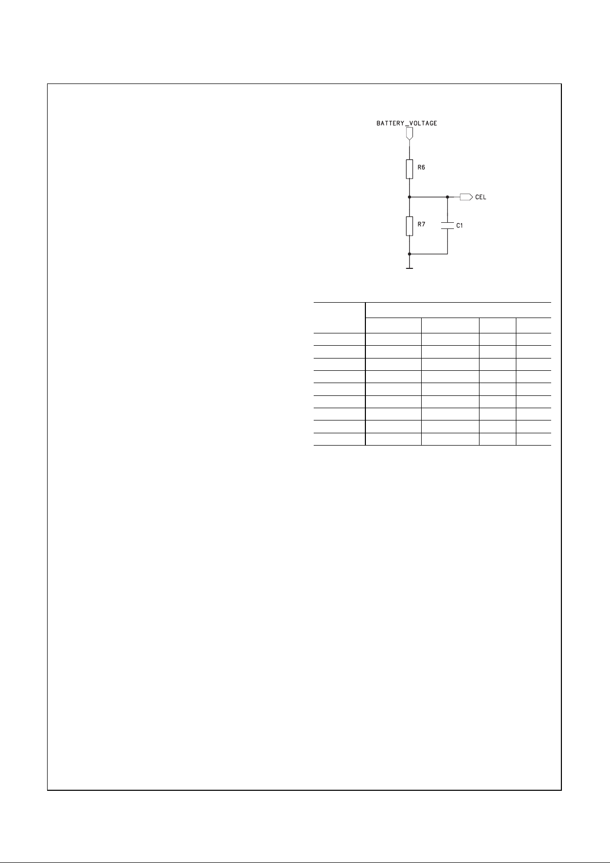
4.3.1 Maximum Battery Voltage
The maximum battery voltage corresponds to the number of
battery cells. The resistor network in the figure below scales
the battery voltage to a level suitable for the LM3647. For NiCd/Ni-MH batteries the tolerance of the network is not critical, and only defines the maximum battery voltage (which is
used as a backup termination method). For Li-Ion batteries
the network must be more accurate, and resistors with low
tolerances must be used (1% or better).
Ni-Cd/Ni-MH:
Each battery cell is at nominal voltage 1.2V, but the critical
voltage is rather the maximum voltage per cell specified at
1.85V. By multiplying the number of cells with the maximum
cell voltage, the Maximum Battery Voltage is achieved.
When the maximum battery voltage has been determined,
the voltagedivider network can bedimensioned using the following formula:
Resistor network selection Quick Guide:
Example: A standard 9V Ni-Cd block battery is composed of
6 small Ni-Cd cells and therefore have a nominal voltage of
7.2V. See table above for resistor values.
Li-Ion:
The voltage divider network for Li-Ion must be selected with
great care for maximum utilization of the batteries. Li-Ion battery cells have a nominal voltage of 3.6V or 3.7V and the
maximumvoltageper cell is specified at 4.1V or 4.2V respectively.By multiplying the number of battery cells with the maximum cell voltage, it is possible to determine the Maximum
Voltage of the Battery Pack.When the maximumbattery voltage has been determined, the voltage divider network has to
be dimensioned using the following formula:
(2.740V if SEL3 is set to Vcc)
The LM3647 supports two different user selectable battery
input voltages on the cell pins. These are 2.675V (SEL3 tied
to GND) and 2.740V (SEL3 tied to Vcc). This selection pin
can be used to configure the charger to handle both 3.6V and
3.7V Li-Ion-cells, without changing resistor values. SEL3 can
also be used if there is problem in finding the right values in
the resistor network.
MaximumBatteryVoltage
R7
R6 R7+()
------------------------ -
× CEL= 3.017V=
No. of Cells
Ni-Cd/Ni-MH
Normal Max R6 R7
2 2.4V 3.7V
3 3.6V 5.55V
4 4.8V 7.4V 16k 11k
5 6V 9.25V 62k 30k
6 7.2V 11.1V 15k 5.6k
7 8.4V 12.95V
8 9.6V 14.8V 39k 10k
9 10.8V 16.65V
10 12V 18.5V 22k 3.9k
MaximumBatteryVoltage
R7
R6 R7+()
------------------------ -
× CEL= 2.675V=
Page 7

7 www.national.com
Resistor network selection Quick Guide:
4.3.2 Charge Timeout
The LM3647 uses the charge timeout value as a backup termination method if the normal termination methods fail. The
charge timeout also controls the length of some of the phases, (e.g., the Topping Charge phase). The timeout is selectable between a charge rate of 3.2C down to 0.4C. The table
below shows R-C values and their resulting timeout.
4.3.3 Charge Current
The charge-current is selected by setting the current sensing
resistor and the gain of the differential amplification stage.
The current sensing resistor (R5) should be dimensioned
such that a voltage drop over it is not too small, because the
signal will be more susceptibleto noise and offsets in the amplification-stage. The resistance should not be too large either (especially in high-current applications), because this
will only generate more heat from the component. A suitable
value is one that develops about 50mV across the resistor
when maximum current flows through it.
The current-sensing signal is amplified, inverted and centered on the 2.5V reference by the operational amplifier and
fed into the CS pin on the LM3647. The amplification stage
must be dimensioned by setting the appropriate ratio between R1 (R3) and R2 (R4). The figure below is dimensioned
for a maximum current of about 1.1A. This was dimensioned
using the following formula:
4.3.4 Dimensioning the reset circuitry
The reset-circuitry is designed to hold the RESET-pin until
the power supply to the LM3647 has stabilized. The RC-network (R21 and C4) should be dimensioned in the following
way:
The diode D2 discharges the capacitance C4 when power
loss occurs. The resistor R20 is used to protect the SYSOKpin,and its value is not critical (typical value is 2kΩ). The con-
No. of Cells
Li-Ion (3.6V cell)
Normal Max R6 R7
1 3.6V 3.675V 16k 30k
2 7.2V 7.35V 62k 30k
3 10.8V 11.025V 27k 7.5k
4 14.4V 14.7V 22k 3.9k
No. of Cells
Li-Ion (3.7V cell)
Normal Max R6 R7
1 3.7V 3.74V 16k 30k
2 7.4V 7.48V 62k 30k
3 11.1V 11.22V 27k 7.5k
4 14.8V 14.96V 22k 3.9k
R Value C Value Appropriate Charge Rates
100 kΩ internal 3.2C
100 kΩ 10 nF 2.4C
100 kΩ 15 nF 1.4C
100 kΩ 22 nF 1.2C
100 kΩ 33 nF 0.9C
100 kΩ 47 nF 0.7C
100 kΩ 68 nF 0.5C
100 kΩ 100 nF 0.4C
R1
R2
MaxCurrent
R2()R1()⁄
R5
---------------------------
=
R1 R3= R2 R4=
R2 5.1kΩ= R1 100kΩ= R5 0.047Ω=
MaxCurrent 1.09Ampere≈
R21 C4×()5xPowerSupplyRiseTime>
Page 8

8 www.national.com
nection between RESET and SYSOK is optional but highly
recommended for safe operation of the LM3647.
4.3.5 Dimensioning the RCIN circuitry
The RC-circuitry is designed to time the charger so it charges
and regulates at the correct frequency. The values of the R
and C are important, because a change in the RC-value
gives a higher or lower operating frequency which affects
charge quality. The capacitance should be a ceramic type
and preferablyan NP0 type, which gives the least frequency
deviation with temperature change.
4.3.6 Dimensioning the DISCHARGE circuitry
The discharge-circuitry controls the discharge rate during the
discharge phase (if used). The discharge output turns on the
transistor Q2, and a current flows from the battery through
the discharge resistor R8. The current through R8 depends
on battery voltage and the value of R8. This value depends
on the maximum discharge rate for the battery-pack. The approximate value can be calculated using the formula below:
The resistor R7 keeps the transistor Q2 off until the LM3647
has been powered up and is in control of the circuitry.
4.3.7 BUZZER output circuitry
The buzzer-circuitry turns the transistor Q3 on when the
buzzershouldsound. If the current consumption forthebuzzer is lower than 0.3mA then the buzzer may be directly connected to the BUZZER-pin. Please note that the BUZZERpin does not generate a PWM-signal, such buzzers must
havetheir own drive-circuitry. If an electromagnetic buzzer is
used, then the transistor mayneed a reverse-biaseddiode to
protect it from harmful voltage spikes.
4.3.8 PWM filter circuitry
The PWM-pin can either output a fast PWM-signal, or a slow
on/offoutput (for controlling external constant current source,
Ni-Cd/Ni-MH mode only).
Fast PWM-mode:
The RC-network R6, C9 and R5, C1||C2 lowpass-filters the
PWM-signal from the LM3647 to a DC-level that is fed into
the operational amplifier. The resistor R22 is required to preventDC-outputbeforethe LM3647 has control of the RC-networks.
R8
MaximumBatteryVoltage
MaximumDisch eRatearg
-------------------------------------------------------------------
≈
Q3
Page 9

9 www.national.com
Slow PWM-mode:
The PWM-pin turns the external current source on and off at
a rate of 0.1Hz. (This example is just one of many possible
design solutions.) The PWM-pin (SLOW_PWM) turns the
transistor Q1 on and off. When the transistor is off the current
source is on, and when the transistor is on the current source
is off (V_OUT at approximate 0.7V). The value of R1 depends on the size of the charge current (see formula):
The PWM duty cycle for the different charge cycles are listed
below:
4.3.9 User Interface
The user interface consists of three LEDs and one buzzer.
The LEDs have four different states:
On, off, slow flash (~1 Hz) and fast flash (~10 Hz). The buzzer has three different states: off, one short beep (~100ms)
and one long beep (~1s).
The user interface is designed in a flexible way. Use of the
buzzeror the LEDs is optional, depending on design requirements. It is possible to use the LM3647 with one, two or all
three LEDs.
A single Charged Status LED can be implemented with a 2input NAND gate on LED1 and LED3. In this implemention,
note that a pull-up resistor is required on LED1 and LED3.
Ni-Cd/Ni-MH User Interface Scheme
C2
1uF
C1
1uF
C9
1uF
R5
10k
R6
10k
R22
10k
PWM
DC-PWM
CURRENT-LIMITER
I
out
=V
d
= Voltage Drop Across D1
1.25 - V
d
R1
Charge Phase: PWM Duty Cycle:
Soft Start 10%
Fast Charge 100%
Topping Charge 10%
Maintenance Charge 5%
Charge phase LED1 status LED2 status LED3 status Buzzer status
No battery Off Off Off Off
New battery / Temp-test Fast flash Off Off Short beep
Softstart charge Slow flash Off Off Off
Charging On Slow flash Off Off
Topping charge On Fast flash Off Off
Maintenance On Off On Long beep
Discharge Off Slow flash Off Off
Temperature error 2 Fast flashes Off On Short beep
Error Fast flash Off Fast flash Short beep
Page 10

10 www.national.com
Li-Ion User Interface Scheme
Charge phase LED1 status LED2 status LED3 status Buzzer status
No battery Off Off Off Off
New battery / Temp-test Fast flash Off Off Short beep
Qualification charge Slow flash Off Off Off
Charging CC On Slow flash Off Off
Charging CV On Fast flash Off Off
Maintenance On Off On Long beep
Temperature error 2 Fast flashes Off On Short beep
Error Fast flash Off Fast flash Short beep
Page 11

11 www.national.com
4.4 Typical Circuit Configurations
4.4.1 Common Circuitry used for both Ni-Cd/Ni-MH and Li-Ion
Page 12

12 www.national.com
4.4.2 Circuitry used only for Ni-Cd/Ni-MH
Page 13

13 www.national.com
4.4.3 Circuitry used for Li-Ion (can also be used for Ni-Cd and Ni-MH if those chemestries are to be supported with the
same charger)
Note: D7 is required to protect Q4 from reverse current.
Page 14

14 www.national.com
4.4.4 Li-Ion Application Example
Figure 1. Li-lon Charger Application
UNREGULATED_DC (MAX20V)
14
Page 15

15 www.national.com
4.4.5 Ni-Cd/Ni-MH, Application Example
Figure 2. Ni-Cd/NiMH Charger Application
UNREGULATED_DC (MAX20V)
15
Page 16

16 www.national.com
4.5 Recommended dimensioning for the NTC
The voltage at TEMP-input must be between 2.2V and 0.5V
for the charger to start. While charging the voltage, must stay
between 3.0V (maximum temperature) for Li-Ion, or 3.15V
(maximum temperature) for Ni-Cd/Ni-MH, and 0.5V (mini-
mum temperature) or the charger will register a temperature
fault and abort the charge. These voltages correspond to the
upper and lower limits for the battery pack temperature.
When no NTC is used the TEMP-input pin must be biased to
a voltage level between 2.2V and 0.5V.
Typical configuration curve, (NTC characteristics: 3kΩ @ 25°C, β=3988:
0
0.5
1
1.5
2
2.5
3
3.5
-10-505101520253035404550
Temperature in °C
Voltage at Temperature input
Page 17

National does not assume any responsibility for use of any circuitry described, no circuit patent licenses are implied, and National reserves the right, at any time without notice, to change said circuitry or specification.
LIFE SUPPORT POLICY
NATIONAL’S PRODUCTS ARE NOT AUTHORIZED FOR USE AS CRITICAL COMPONENTS IN LIFE SUPPORT
DEVICES OR SYSTEMS WITHOUT THE EXPRESS WRITTEN APPROVAL OF THE PRESIDENT OF NATIONAL
SEMICONDUCTOR CORPORATION. As used herein:
1. Life support devices or systems are devices or systems
which,(a) are intended for surgical implant into thebody,
or (b) support or sustain life, and whose failure to perform,whenproperlyused in accordance withinstructions
for use provided in the labeling, can be reasonably expected to result in a significant injury to the user.
2. A critical component is any component of a life support
device or system whose failure to perform can be reasonably expected to cause the failure of the life support
device or system, or to affect its safety or effectiveness.
National Semiconductor
Corporation
Tel: 1-800-272-9959
Fax: 1-800-737-7018
Email: support@nsc.com
National Semiconductor
Europe
Fax: +49 (0) 180-530 85 86
Email: europe.support@nsc.com
Deutsch Tel: +49 (0) 69 9508 6208
English Tel: +44 (0) 870 24 0 2171
Francais Tel: +33 (0) 1 41 91 8790
National Semiconductor
Japan Ltd.
Tel: 81-3-5620-6175
Fax: 81-3-5620-6179
www.national.com
National Semiconductor
Asia Pacific
Customer Response Group
Tel: 65-254-4466
Fax: 65-250-4466
Email: sea.support@nsc.com
LM3647 Universal Battery Charger for Li-Ion, Ni-MH and Ni-Cd Batteries
Physical Dimensions inches (millimeters) unless otherwise noted
Molded SO Wide Body Package (WM)
Order Number LM3647IM
See NS Package Number M20B
 Loading...