

Page 1
LM363 Precision Instrumentation Amplifier
General Description
The LM363 is a monolithic true instrumentation amplifier. It
requires no external parts for fixed gains of 10, 100 and
1000. High precision is attained by on-chip trimming of offset voltage and gain. A super-beta bipolar input stage gives
very low input bias current and voltage noise, extremely low
offset voltage drift, and high common-mode rejection ratio.
A two-stage amplifier design yields an open loop gain of
10,000,000 and a gain bandwidth product of 30 MHz, yet
remains stable for all closed loop gains. The LM363 operates with supply voltages from
g
5V tog18V with only
1.5 mA current drain.
The LM363’s low voltage noise, low offset voltage and offset voltage drift make it ideal for amplifying low-level, lowimpedance transducers. At the same time, its low bias current and high input impedance (both common-mode and
differential) provide excellent performance at high impedance levels. These features, along with its ultra-high common-mode rejection, allow the LM363 to be used in the
most demanding instrumentation amplifier applications, replacing expensive hybrid, module or multi-chip designs. Because the LM363 is internally trimmed, precision external
resistors and their associated errors are eliminated.
The 16-pin dual-in-line package provides pin-strappable
gains of 10, 100 or 1000. Its twin differential shield drivers
eliminate bandwidth loss due to cable capacitance. Compensation pins allow overcompensation to reduce bandwidth and output noise, or to provide greater stability with
capacitive loads. Separate output force, sense and reference pins permit gains between 10 and 10,000 to be programmed using external resistors.
On the 8-pin metal can package, gain is internally set at 10,
100 or 500 but may be increased with external resistors.
The shield driver and offset adjust pins are omitted on the
8-pin versions.
The LM363 is rated for 0
Features
Y
Offset and gain pretrimmed
Y
12 nV/0Hz input noise (Ge500/1000)
Y
130 dB CMRR typical (Ge500/1000)
Y
2 nA bias current typical
Y
No external parts required
Y
Dual shield drivers
Y
Can be used as a high performance op amp
Y
Low supply current (1.5 mA typ)
Cto70§C.
§
LM363 Precision Instrumentation Amplifier
April 1991
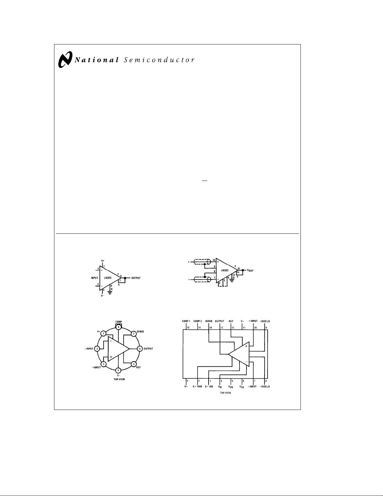
Typical Connections
8-Pin Package
TL/H/5609– 1
16-Pin Package
Ge10 2, 3, 4, open
e
100 3 –4 shorted
G
e
1000 2 –4 shorted
G
TL/H/5609– 33
Connection Diagrams
Metal Can Package 16-Pin Dual-In-Line Package
Order Number LM363H-10,
LM363H-100 or LM363H-500
See NS Package Number H08C
C
1995 National Semiconductor Corporation RRD-B30M115/Printed in U. S. A.
TL/H/5609
Order Number 363D
See NS Package Number D16C
TL/H/5609– 2
Page 2
Absolute Maximum Ratings (Note 5)
If Military/Aerospace specified devices are required,
please contact the National Semiconductor Sales
Office/Distributors for availability and specifications.
g
g
18V
g
10V
20 mA
Supply Voltage
Differential Input Voltage
Input Current
Input Voltage Equal to Supply Voltage
Reference and Sense Voltage
Lead Temp. (Soldering, 10 sec.) 300§C
ESD rating to be determined.
LM363 Electrical Characteristics (Notes 1 and 2)
LM363
Parameter Conditions
Typ Limit Limit
FIXED GAIN (8-PIN)
Input Offset Voltage Ge500 30 150 400 mV
e
G
100 50 250 700 mV
e
G
10 0.5 2.5 6 mV
Input Offset Voltage Drift Ge500 1 4 mV/§C
e
G
100 2 8 mV/§C
e
G
10 20 75 mV/§C
Gain Error Ge500 0.1 0.8 0.9 %
g
(
10V Swing, 2 kX Load) Ge100 0.07 0.7 0.8 %
e
G
10 0.05 0.6 0.7 %
PROGRAMMABLE GAIN (16-PIN)
Input Offset Voltage Ge1000 50 250 500 mV
e
G
100 100 450 900 mV
e
G
10 1 3.5 8 mV
Input Offset Voltage Drift Ge1000 1 5 mV/§C
e
G
100 2 10 mV/§C
e
G
10 10 100 mV/§C
Gain Error Ge1000 2.0 3.0 3.5 %
g
(
10V Swing, 2 kX Load) Ge100 0.1 0.7 0.8 %
e
G
10 0.6 2.0 2.3 %
FIXED GAIN AND PROGRAMMABLE
Gain Temperature Coefficient Ge1000 40 ppm/§C
e
G
500 20 ppm/§C
e
G
100, 10 10 ppm/§C
Gain Non-Linearity Ge10, 100 0.01 0.03 0.04 %
g
(
10V Swing, 2 kX Load) Ge500, 1000 0.01 0.05 0.06 %
Tested Design
(Note 3) (Note 4)
g
Units
25V
2
Page 3
LM363 Electrical Characteristics (Continued) (Notes 1 and 2)
LM363
Parameter Conditions
Typ Limit Limit
Common-Mode Rejection Ge1000, 500 130 114 104 dB
Ratio (
b
10VsV
s
10V) Ge100 120 94 84 dB
CM
Ge10 105 90 80 dB
Positive Supply Rejection Ge1000, 500 130 110 100 dB
Ratio (5V to 15V) G
e
100 120 100 95 dB
e
G
10 100 85 78 dB
Negative Supply Rejection Ge1000, 500 120 100 90 dB
b
Ratio (
5V tob15V) Ge100 106 85 75 dB
e
G
10 86 70 60 dB
Input Bias Current 2 10 20 nA
Input Offset Current 1 3 5 nA
Common-Mode Input 100 8 GX
Resistance
Differential Mode Input Ge1000, 500 0.2 GX
Resistance G
e
100 2 GX
Ge10 20 GX
Input Offset Current Change
b
11VsV
s
13V 20 100 300 pa/V
CM
Reference and Sense 50 kX
Resistance Min 30 27 kX
Max 80 83 kX
Open Loop Gain G
e
1000, 500 10 1 V/mV
CL
Supply Current Positive 1.2 2.4 3.0 mA
Negative 1.6 2.8 3.4 mA
a
b
e
eb
Note 1: These conditions apply unless otherwise noted; V
e
25§C.
T
j
Note 2: Boldface limits are guaranteed over full temperature range. Operating ambient temperature range is 0
Note 3: Guaranteed and 100% production tested.
Note 4: Guaranteed but not 100% tested. These limits are not used in determining outgoing quality levels.
Note 5: Maximum rated junction temperature is 100
for the ceramic DIP (D).
15V, V
C for the LM363. Thermal resistance, junction to ambient, is 150§C/W for the TO-99(H) package and 100§C/W
§
15V, V
e
0V, R
CM
L
Tested Design
(Note 3) (Note 4)
e
2kX, reference pin grounded, sense pin connected to output and
Cto70§C for the LM363.
§
Units
3
Page 4
Typical Performance Characteristics T
Parameter
e
25§C
A
Fixed Gain and Programmable
1000/500 100 10
Input Voltage Noise, rms, 1 kHz 12 18 90 nV/SHz
Input Voltage Noise (Note 6) 0.4 1.5 10 mVp-p
Input Current Noise, rms, 1 kHz 0.2 0.2 0.2 pA/SHz
Input Current Noise (Note 6) 40 40 40 pAp-p
Bandwidth 30 100 200 kHz
Slew Rate 1 0.36 0.24 V/ms
Settling Time, 0.1% of 10V 70 25 20 ms
Offset Voltage Warm-Up Drift (Note 7) 5 15 50 mV
Offset Voltage Stability (Note 8) 5 10 100 mV
Gain Stability (Note 8) 0.01 0.005 0.05 %
Note 6: Measured for 100 seconds in a 0.01 Hz to 10 Hz bandwidth.
Note 7: Measured for 5 minutes in still air, V
a
b
e
eb
15V, V
15V. Warm-up drift is proportionally reduced at lower supply voltages.
Units
Common-Mode Input
Voltage Limit
Output Swing Referred to
Supplies
Supply Current vs Supply
Voltage
Supply Current vs
Temperature
Input Bias Current vs
Temperature
Input Offset Current vs
Temperature
TL/H/5609– 3
4
Page 5
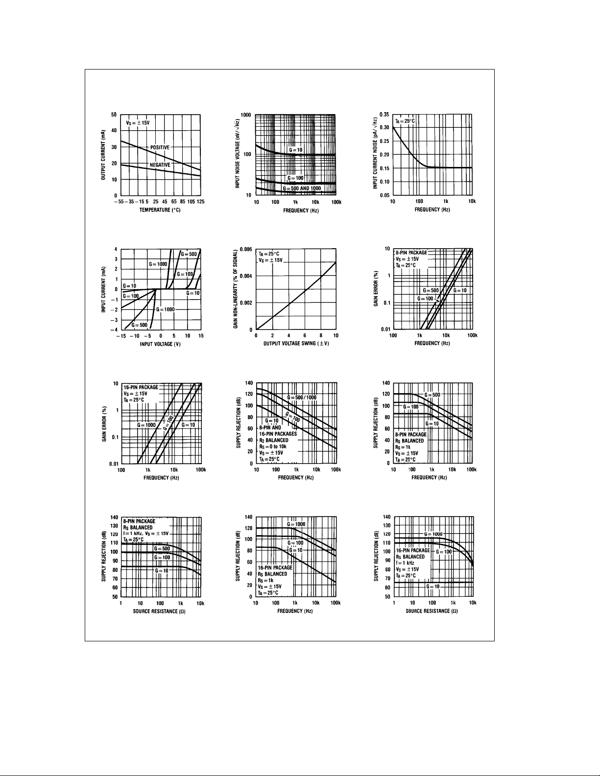
Typical Performance Characteristics (Continued)
Output Current Limit Input Noise Voltage Input Current Noise
Input Current vs Voltage
Overdrive Gain Non-Linearity Gain Error vs Frequency*
*Trimmed to zero at 100 Hz
Gain Error vs Frequency* Rejection Rejection
Positive Power Supply Negative Power Supply
*Trimmed to zero at 100 Hz
Negative Power Supply Negative Power Supply Negative Power Supply
Rejection Rejection Rejection
5
TL/H/5609– 4
Page 6
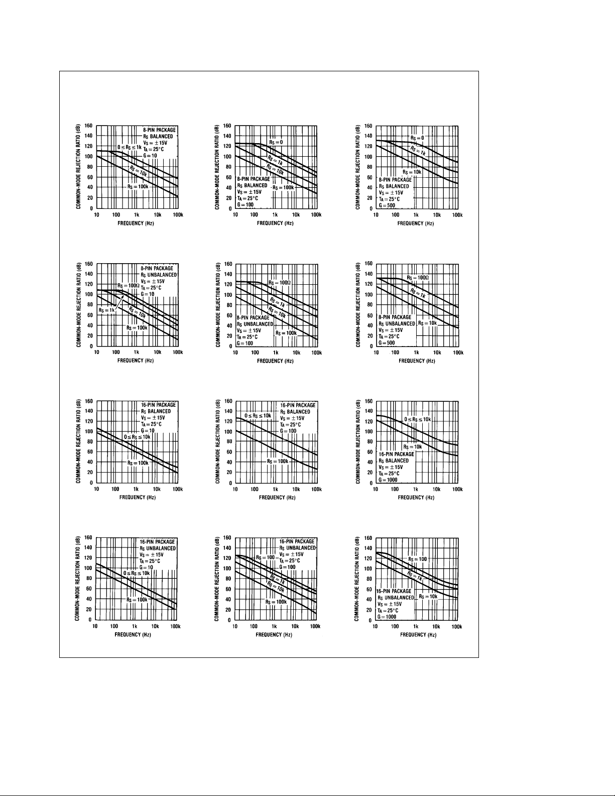
Typical Performance Characteristics (Continued)
CMRR with Balanced CMRR with Balanced CMRR with Balanced
Source Resistance Source Resistance Source Resistance
CMRR with Unbalanced CMRR with Unbalanced CMRR with Unbalanced
Source Resistance Source Resistance Source Resistance
CMRR with Balanced CMRR with Balanced CMRR with Balanced
Source Resistance Source Resistance Source Resistance
CMRR with Unbalanced CMRR with Unbalanced CMRR with Unbalanced
Source Resistance Source Resistance Source Resistance
TL/H/5609– 5
6
Page 7
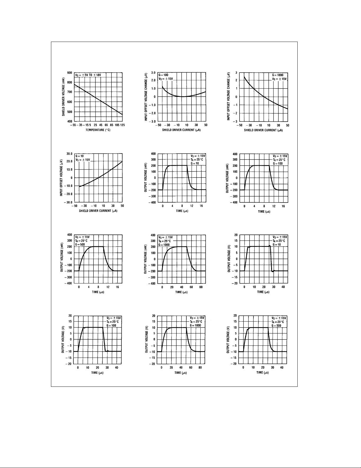
Typical Performance Characteristics (Continued)
Shield Driver Bias Voltage Shield Driver Loading Error Shield Driver Loading Error
Shield Driver Loading Error Response
Small Signal Transient
Response
Large Signal Transient
Response
Small Signal Transient
Small Signal Transient
Response
Large Signal Transient
Response
Small Signal Transient
Response
Large Signal Transient
Response
Large Signal Transient
Response
TL/H/5609– 6
7
Page 8

Simplified Schematic (pin numbers in parentheses are for 8-pin package)
TL/H/5609– 7
Theory of Operation
Referring to the Simplified Schematic, it can be seen that
the input voltage is applied across the bases of Q1 and Q2
and appears between their emitters. If R
ance across these emitters, a differential current equal to
V
IN/RE1-2
stage amplifier shown maintains Q1 and Q2 at equal collec-
flows from Q1’s emitter to Q2’s. The second
tor currents by negative feedback to Q4. The emitter currents of Q3 and Q4 must therefore be unbalanced by an
amount equal to the current flow across R
eR5a
R
E3-4
of Q4 to Q3 is equal to
R6, the differential voltage across the emitters
V
IN
c
R
E 1-2
E3-4
R
.
is the resist-
E1-2
E1-2
. Defining
This voltage divided by the attenuation factor
R4
R3aR4
e
R1aR2
R2
is equal to the output-to-reference voltage. Hence, the overall gain is given by
V
R3aR4
OUT
e
e
G
V
IN
R4
R
E3-4
c
.
R
E1-2
8
Page 9

Application Hints
The LM363 was designed to be as simple to use as possible, but several general precautions must be taken. The differential inputs are directly coupled and need a return path
to power supply common. Worst-case bias currents are only
10 nA for the LM363, so the return impedance can be as
high as 100 MX. Ground drops between signal return and IC
supply common should not be ignored. While the LM363
has excellent common-mode rejection, signals must remain
within the proper common-mode range for this specification
to apply. Operating common-mode range is guaranteed
b
from
10V toa10V withg15V supplies.
The high-gain (500 or 1000) versions have large gain-bandwidth products (15 MHz or 30 MHz) so board layout is fairly
critical. The differential input leads should be kept away
from output force and sense leads, especially at high impedances. Only 1 pF from output to positive input at 100 kX
source impedance can cause oscillations. The gain adjust
leads on the 16-pin package should be treated as inputs
and kept away from the output wiring.
POWER SUPPLY
The LM363 may be powered from split supplies from
g
to
18V (or single-ended supplies from 10V to 36V). Positive supply current is typically 1.2 mA independent of supply
voltage. The negative supply current is higher than the positive by the current drawn through the voltage dividers for the
reference and sense inputs (typ 600 mA total). The LM363’s
excellent PSRR often makes regulated supplies unnecessary. Actually, supply voltage can be as low as 7V total but
PSRR is severely degraded, so that well-regulated supplies
are recommended below 10V total. Split supplies need not
be balanced; output swing and input common-mode range
will simply not be symmetrical with unbalanced supplies. For
example, at
range is typically
to
a
12V andb5V supplies, input common-mode
a
b
4V.
10.5V tob2V and output swing isa11V
When using ultra-low offset versions, best results are ob-
g
tained at
set voltage is guaranteed within 150 mVat
Running at
ror of 10V (
15V supplies. For example, the LM363-500’s off-
g
5V results in a worst-case negative PSRR er-
b
15V tob5V) multiplied by 3.2X10
g
or 32 mV, increasing the worst-case offset. Positive PSRR
results in another 10 mV worst-case change.
INPUTS
The LM363 input circuitry is depicted in the Simplified Schematic. The input stage is run relatively rich (50 mA) for low
voltage noise and wide bandwidth; super-beta transistors
and bias-current cancellation (not shown) keep bias currents low. Due to the bias-current cancellation circuitry, bias
current may be either polarity at either input. While input
current noise is high relative to bias current, it is not significant until source resistance approaches 100 kX.
Input common-mode range is typically from 3V above V
1.5V below V
a
, so that a large potential drop between the
input signal and output reference can be accommodated.
However, a return path for the input bias current must be
provided; the differential input stage is not isolated from the
supplies. Differential input swing in the linear region is equal
to output swing divided by gain, and typically ranges from
1.3V at G
e
10 to 13 mV at Ge1000.
Clamp diodes are provided to prevent zener breakdown and
resulting degradation of the input transistors. At large input
g
5V
15V at 25§C.
b
6
(110 dB)
b
overdrives these diodes conduct, greatly increasing input
currents. This behavior is illustrated in the I
the Typical Performance Characteristics. (The graph is not
symmetrical because at large input currents a portion of the
current into the device flows out the V
The input protection resistors allow a full 10V differential
input voltage without degradation even at G
voltages more than one diode drop below V
drops above V
a
input, current increases rapidly. Diode
b
terminal.)
vs VINplot in
IN
e
1000. At input
b
or two diode
clamps to the supplies, or external resistors to limit current
to 20 mA, will prevent damage to the device.
REFERENCE AND SENSE INPUTS
The equivalent circuit is shown in the schematic diagram.
Limitations for correct operation are as follows. Maximum
differential
cally
swing between reference and sense pins is typi-
g
15V (g10V guaranteed). If this limit is exceeded, the
sense pin no longer controls the output, which then pegs
high or low. The
b
V
. (This is permissible because R2 and R4 are returned to
a node biased higher than V
negative
common-mode limit is 1.5V below
b
.) If large
positive
voltages are
applied to the reference and sense pins, the common-mode
range of the signal inputs begins to suffer as the drop
across R13 and R16 increases. For example, at
plies, V
b
range drops to
pins can be as much as 10V above V
ed signal common-mode range (
e
REF
12V toa13.5V. At V
e
V
SENSE
b
11V toa13.5V. The reference and sense
0V, signal input range is typically
e
V
REF
SENSE
a
b
10V min) can be tolerat-
g
15V sup-
e
15V, signal input
as long as a restrict-
ed.
For maximum bipolar output swing at
g
15V supplies, the
reference pin should be returned to a voltage close to
ground. At lower supply voltages, the reference pin need
not be halfway between the supplies for maximum output
swing. For example, at V
grounding the reference pin still allows a
a
ea
12V and V
a
b
eb
5V,
11V tob4V
swing. For single-supply systems, the reference pin can be
tied to either supply if a single output polarity is all that is
required. For a bipolar input and output, create a low impedance reference with an op amp and voltage divider or a
regulator (e.g., LM336, LM385, LM317L). This forms the reference for all succeeding signal-processing stages. (Don’t
connect the reference terminal directly to a voltage divider;
this degrades gain error.) See
to
a. Usual configuration maximizes bipolar output swing.
b. Unequal supplies, output ground referred. Full output swing pre-
served referred to supplies.
Figure 1
.
TL/H/5609– 8
FIGURE 1. Reference Connections
9
Page 10

Application Hints (Continued)
c. Single Supply, Unipolar Output d. Single Supply, Bipolar Output
FIGURE 1. Reference Connections (Continued)
OUTPUTS
The LM363’s output can typically swing within 1V of the
supplies at light loads. While specified to drivea2kXload
g
to
10V, current limit is typically 15 mA at room temperature. The output can stably drive capacitive loads up to
400 pF. For higher load capacitance, the amplifier may be
overcompensated (see COMPENSATION section, following). The output may be continuously shorted to ground
without damaging the device.
OFFSET VOLTAGE
The LM363’s offset voltage is internally trimmed to a very
low value. Note that data sheet values are given at
e
T
25§C, V
j
tions, warm-up drift, temperature drift, common-mode rejec-
CM
e
0V and V
a
b
e
e
V
15V. For other condi-
tion and power supply rejection must be taken into account.
Warm-up drift, due to chip and package thermal gradients, is
an effect separate from temperature drift. Typical warm-up
drift is tabulated in the Electrical Characteristics; settling
time is approximately 5 minutes in still air. At load currents
up to 5 mA, thermal feedback effects are negligible
s
(DV
2mVatGe1000).
OS
Care must be taken in measuring the extremely low offset
voltages of the high gain amplifiers. Input leads must be
held isothermal to eliminate thermocouple effects. Oscillations, due to either heavy capacitive loading or stray capacitance from input to output, can cause erroneous readings.
In either case, overcompensation will help. High frequency
noise fed into the inputs may be rectified internally, and pro-
TL/H/5609– 9
duce an offset shift. A simple low-pass RC filter will usually
cure this problem (
Figure 2
). Use film type resistors for their
low thermal EMF. In highly noisy environments, LC filters
can be substituted for increased RF attenuation.
FIGURE 2. Low Pass Filter Prevents RF Rectification
TL/H/5609– 10
Instrumentation amplifiers have both an input offset voltage
(V
) and an output offset voltage (V
IOS
referred offset voltage (V
tation amplifier gain (G) as follows: V
) is related to the instrumen-
OSRTI
G. The offset voltage given in the LM363 specifications is
). The total input-
OOS
e
V
OSRTI
IOS
a
V
OOS
the total input-referred offset. As long as only one gain is
used, offset voltage can be nulled at either input or output
as shown in
used at multiple gain settings, both V
be nulled to get minimum offset at all gains, as shown in
Figure 3c
output at G
Figures 3a
. The correct procedure is to trim V
e
10, then trim V
and3b. When the 16-pin device is
and V
IOS
at Ge1000.
IOS
OOS
OOS
should
for zero
/
FIGURE 3. Offset Voltage Trimming
10
TL/H/5609– 11
Page 11

Application Hints (Continued)
Because the LM363’s offset voltage is so low to begin with,
offset nulling has a negligible effect on offset temperature
drift. For example, zeroing a 100 mV offset, assuming external
resistor TC of 200 ppm/
TC, results in an additional drift component of 0.08 mV/
For this reason, drift specifications are guaranteed, with or
C and worst-case internal resistor
§
C.
§
without external offset nulling.
GAIN ADJUSTMENT
Gain may be increased by adding an external voltage divider between output force and sense and reference; the preferred connection is shown in
sense and reference pins look like 50 kX (
Figure 4
. Since both the
g
20 kX)toVb,
impedances presented to both pins must be equal to avoid
offset error. For example, a 100X imbalance can create a
R1 and R2 should be as low as possible to avoid errors due to 50 k X
input impedance of reference and sense pins. Total resistance
a
2R1) should be above 4 kX, however, to prevent excessive load
(R2
TL/H/5609– 12
on the LM363 output. The exact formula for calculating gain (G) is:
G
G
The last term may be ignored in applications where gain accuracy is not
critical. The table below gives suggested values for R1 and R2 along
with the calculated error due to ‘‘closest value’’ standard 1% resistors.
Total gain error tolerance includes contributions from LM363 G
and resistor tolerance (
every case.
Pinout shown is for 16-pin package. This same technique can also be
used with 8-pin versions.
e
G
e
O
2R1
a
1
O
R2
#
preset gain
Gain Increase 1.522.5345678910
R1 1.21k 1.21k 2k 2k 1.78k 2k 2.49k 2.94k 3.48k 3.92k 4.42k
R2 5k 2.49k 2.74k 2.05k 1.21k 1k 1k 1k 1k 1k 1k
Error (typ)
a
0.6%b0.2% 0
b
0.3%b0.6%a0.8%a0.5%b0.9%a0.4%b0.9%b0.7%
FIGURE 4. Increasing Gain
worst-case output offset of 50 mV, creating an input-referred error of 5 mV at G
e
10 or 50 mVatGe1000.
Increasing gain this way increases output offset error. An
LM363H-100 may have an output offset of 5 mV, resulting in
input referred offset component of 50 mV. Raising the gain
to 200 yields a 10 mV error at the output and changes input
referred error by an additional 50 mV.
External resistors connected to the reference and sense
pins can only
ance is not critical, the technique in
increase
the gain. If ultra-low output imped-
Figure 5
trim the gain to nominal value. Alternatively, the V
ment terminals on the 16-pin package may be used to trim
the gain (
R1
a
50k
J
g
1%) and works out to approximately 2.5% in
Figure 10b
).
error
O
can be used to
adjust-
OS
FIGURE 5. Adjusting Gain, Alternate Technique
11
Pinout shown is for 8-pin versions.
This same technique can also be used
with 16-pin version.
TL/H/5609– 13
Page 12

Application Hints (Continued)
COMPENSATION AND OUTPUT CLAMPING
The LM363 is internally compensated for unity feedback
from output to sense. Increasing gain with external dividers
will decrease the bandwidth and increase stability margin.
Without external compensation, the amplifier can stably
drive capacitive loads up to 400 pF. When used as an op
amp (sense and reference pins grounded, feedback to inverting input), the LM363 is stable for gains of 100 or more.
For greater stability, the device may be over-compensated
as in
Figure 6
tion components along with the resulting changes in large
and small signal bandwidth for the 8-pin and 16-pin packages, respectively.
Note that the RC network from pin 8 of the 8-pin device to
ground has a large effect on power bandwidth, especially at
low gains. The Miller capacitance utilized for overcompensating the 16-pin device permits higher slew rate and larger
load capacitance for the same bandwidth, and is preferred
when bandwidth must be greatly reduced (e.g., to reduce
output noise).
. Tables I and II depict suggested compensa-
TABLE I. Overcompensation on 8-Pin Package
Compensation Network 3 dB Bandwidth Capacitive
Gain
500 1000 pF, 5k 45 1.8k 800
100 1000 pF, 5k 80 1.8k 1200
10 1000 pF, 5k 90 1.8k 1200
*Also stable for C
²
Pin 15 to ground on 16-pin package
(Pin 8 to Ground)
Ð 125 100k 400
100 pF, 15k 95 15k 600
0.01 mF,500X 10 200 1000*
0.1 mF 1 20 1000*
Ð 240 100k 400
100 pF, 15k 170 15k 900
0.01 mF, 500X 20 200 1600*
0.1 mF 2 20 2000*
Ð 240 100k 400
100 pF, 15k 170 15k 900
0.01 mF, 500X 20 200 1600*
0.1 mF 2 20 2000*
t
0.05 mF
L
Small Signal Power Maximum
²
Bandwidth (g10V Swing) Load
TABLE II. Overcompensation on 16-Pin Package
Gain Capacitor
1000 100 pF 2.5k 2.5k 2500*
100 100 pF 7.5k 7.5k 2000*
*Also stable for C
Compensation
(Pin 15 to 16)
Ð 45k 45k 1000*
10 pF 16k 16k 2000*
1000 pF 250 250 3000*
0.01 mF 25 25 3000*
Ð 140k 100k 900
10 pF 50k 50k 1600
1000 pF 750 750 2000*
0.01 mF 75 75 2000*
Ð 180k 90k 600
10 100 pF 9k 9k 1600
10 pF 60k 50k 1100
1000 pF 900 900 2000*
0.01 mF 90 90 2000*
t
0.05 mF
L
Small Signal Power Maximum
3 dB Bandwidth Capacitive
Bandwidth (
(Hz) (Hz) (pF)
Heavy Miller overcompensation on the 16-pin package can
degrade AC PSRR. A large capacitor between pins 15 and
16 couples transients on the positive supply to the output
buffer. Since the amplifier bandwidth is severely rolled off it
cannot keep the output at the correct state at moderate
frequencies. Hence, for good PSRR, either keep the Miller
capacitance under 1000 pF or use the pin 15-to-ground
compensation shown in Table I.
FIGURE 6. Overcompensation
(kHz) (Hz) (pF)
g
10V Swing) Load
12
TL/H/5609– 14
Page 13

Application Hints (Continued)
Because the LM363’s output voltage is approximately one
diode drop below the voltage at pin 15 (pin 8 for the 8-pin
device), this point may be used to limit output swing as seen
in
Figure 7a
that zeners must have a sharp breakdown to clamp accurately. Alternatively, a diode tied to a voltage source could
be used as in
. Current available from this pin is only 50 mA, so
Figure 7b
.
50 pF to ground at both shield driver outputs. Do not use
only one shield driver for a single-ended signal as oscillations can result; shield driver to input capacitance must be
roughly balanced (
g
30%). To further reduce noise pickup,
the shielded signal lines may be enclosed together in a
grounded shield. If a large amount of RF noise is the problem, the only sure cure is a filter capacitor at both inputs;
otherwise the RFI may be internally rectified, producing an
offset.
DC loading on the shield drivers should be minimized. The
drivers can only source approximately 40 mA; above this
value the input stage bias voltages change, degrading V
and CMRR. While the shield drivers can sink several mA,
V
may degrade severely at loads above 100 mA (see
OS
Shield Driver Loading Error curve in Typical Performance
OS
Characteristics). Because the shield drivers are one diode
drop above the input levels, unbalanced leakage paths from
shield to input can produce an input offset at high source
impedances. Buffering with emitter-followers (
Figure 8b
) reduces this leakage current by reducing the voltage differential and eliminates any loading on the amplifier.
FIGURE 7. Output Clamp
TL/H/5609– 15
SHIELD DRIVERS
When differential signals are sent through long cables, three
problems occur. First, noise, both common-mode and differential, is picked up. Second, signal bandwidth is reduced by
the RC low-pass filter formed by the source impedance and
the cable capacitance. Finally, when these RC time constants are not identical (unbalanced source impedance
and/or unbalanced capacitance), AC common-mode rejection is degraded, amplifying both induced noise and
‘‘ground’’ noise. Either filtering at the amplifier inputs or
slowing down the amplifier by overcompensating will indeed
reduce the noise, but the price is slower response. The
LM363D’s dual shield drivers can actually increase bandwidth while reducing noise.
The way this is done is by bootstrapping out shield capacitance. The shield drivers follow the input signal. Since both
sides of the shield capacitance swing the same amount, it is
effectively out of the circuit at frequencies of interest.
Hence, the input signal is not rolled off and AC CMRR is not
degraded (
Figure 8
). The LM363D’s shield drivers can handle capacitances (shield to center conductor) as high as
1000 pF with source resistances up to 100 kX.
For best results, identical shielded cables should be used
for both signal inputs, although small mismatches in shield
driver to ground capacitance (
s
500 pF) do not cause problems. At certain low values of cable capacitance (50 pF –
200 pF), high frequency oscillations can occur at high
source resistance (
t
10 kX). This is alleviated by adding
FIGURE 8. Driving Shielded Cables
TL/H/5609– 16
MISCELLANEOUS TRIMMING
The V
pin package may be used to trim the other parameters besides offset voltage, as illustrated in
adjust and shield driver pins available on the 16-
OS
Figure 10
. The bias-current trim relies on the fact that the voltage on the shield
driver and gain setting pins is one diode drop respectively
above and below the input voltage. Input bias current can
be held to within 100 pA over the entire common-mode
range, and input offset current always stays under 30 pA.
The CMRR trims use the shield driver pins to drive the V
adjust pins, thus maintaining the LM363’s ultra-high input
OS
impedance.
13
Page 14

Application Hints (Continued)
If power supply rejection is critical, frequently only the negative PSRR need be adjusted, since the positive PSRR is
more tightly specified. Any or all of the trim schemes of
Figure 10
ter tap of the 100k trimpot is returned to a voltage 200 mV
below V
can be combined as desired. As long as the cen-
a
, the trim schemes shown will not greatly affect
TL/H/5609– 17
VOS. Both the gain and DC CMRR trims can degrade positive PSRR; the positive PSRR can then be nulled out if desired. The correct order of trimming from first to last is bias
current, gain, CMRR, negative PSRR, positive PSRR and
V
.
OS
Top Trace: Cable Shield Grounded
Bottom Trace: Cable Shield Bootstrapped
FIGURE 9. Improved Response using Shield Drivers
FIGURE 10. Other Trims for 16-Pin Package
TL/H/5609– 18
TL/H/5609– 19
14
Page 15

Typical Applications
4 mA-20 mA Two Wire Current Transmitter
The LM329 reference provides excellent line regulation and gain stability. When bridge is balanced
e
4 mA), there’s no drop across R3 and R4, so that gain and offset adjustments are non-in-
(I
OUT
teractive. The LM334 configured as a zero-TC current source supplies quiescent current to circuit.
R11 provides current limiting.
Design Equations
e
I
(I
OS
R6
DI
OUT
e
Gain
DV
when A
V
e
Pick I
334
e
I
I
MAX
334
I
BRIDGE(MAX)
R2
a
a
IR7)#1
R1
A
R2
V
j
X
R1
R3aR4
IN
e
LM363 voltage gain
0.68V
68 mV
a
R9
R10
b
V
2.4V
Z
a
R11
j
I
334-I363-IZ
e
J
aR3a
e
4mA
j
3.8 mA
26 mA
j
R4
j
1.5mA
10 mA
mV
Precision Current Source (Low Output Current)
R1eR2
V
IN
e
I
TL/H/5609– 21
OUT
GR1
,
Precision Voltage to Current Converter (Low Input Voltage)
TL/H/5609– 20
s
V
10V
l
l
IN
R1eR2
e
Req
R1ll50 kX
GV
GV
IN
Req
IN
e
1kX
e
I
OUT
TL/H/5609– 22
15
Page 16

Typical Applications (Continued)
Curvature Corrected Platinum RTD Thermometer
TL/H/5609– 23
*70k and 2k should track to 5 ppm/§C
**Less than 5 ppm/
²
Less than 100 ppm/§C drift
²²
These resistors should track to 20 ppm/§C
³
Equivalent circuit, showing lead resistance
This thermometer is capable of 0.01
a
150§C. A unique trim arrangement eliminates cumbersome trim interactions so that zero, gain, and nonlinearity correction can be trimmed in
one oven trip. Extra op amps provide full Kelvin sensing on the sensor
without adding drift and offset terms found in other designs. A2 is configured as a Howland current pump, biasing the sensor with a fixed
current.
Resistors R2, R3, R4 and R5 from a bridge driven into balance by A1. In
balance, both inputs of A1 are at the same voltage. Since R6
draws equal currents from both legs of the bridge. Any loading of the
R4/R5 leg by the sensor would unbalance the bridge; therefore, both
bridge taps are given to the sensor open circuit voltage and no current
is drawn.
C drift
§
C accuracy overb50§Cto
§
e
R7, A1
*Ultronix 105A wirewound
e
Thermistor
Setpoint stability
Yellow SpringsÝ44032
e
2.5X10
Precision Temperature Controller
TL/H/5609– 24
b
4
C/Hr
§
16
Page 17

Typical Applications (Continued)
Low Frequency Rolloff (AC Coupling)
1
e
f1
2qC1(50 k X)
e
f2
100 f1e100Hz
Reduced DC voltage gain
attenuates offset error and
1/f noise by a factor of 100.
TL/H/5609– 25
Precision Comparator with Balanced Inputs and Variable Offset Boosted Current Source with Limiting
j
t
15 mS at 1 mV overdrive
pd
eV2a
DV
Hysteresis
Offset
OUT
e
DV
G(R1aR2)
e
V
SENSE
g
1.3V range
OUT
0.6V
e
2mV
/G
e
1Hz
R1
I
I
MAX
e
R2
GV
IN
e
O
R2
V
BE
e
R2
j
60 mA
TL/H/5609– 26
Thermocouple Amplifier with Cold Junction Compensation
Input protection circuitry allows
thermocouple to short to 120 V
damaging amplifier.
Calibration:
1) Apply 50 mV signal in place of thermocouple.
Trim R3 for V
2) Reconnect thermocouple. Trim R9 for correct
output.
OUT
17
e
12.25V.
without
AC
TL/H/5609– 27
Page 18

Typical Applications (Continued)
Synchronous Demodulator
*Use square wave drive produced by optical chopper to run LF13333 switch inputs.
Pulsed Bridge Driver/Amplifier
TL/H/5609– 28
TL/H/5609– 29
18
Page 19

Typical Applications (Continued)
**Parallel trim for 28.00×Hge0V
²
Parallel trim for 32.00×Hge4V out
*B.L.H. Electronics
Pressure Transducer,
350X input impedance.
e
Output
Ý
DHF-444114
1 mV/volt excitation/psi
Precision Barometer
TL/H/5609– 30
Removing Large DC Offsets
*Optional bandlimiting to reduce noise.
e
Pick R1C1
f
l
LM363 bias currents flowing into R1 and R2.
R2C2eR3C3/10
1
e
2qf
l
e
0.1 Hz for values shown. Integrator nulls out offset error to
Removing Small DC Offsets
*Optional bandlimiting to reduce noise.
Low frequency break
frequency f
Accommodates out referred offset of several volts. Limit is set by max
differential between reference and sense terminals.
e
l
2qR1C1
1
e
0.01 Hz
TL/H/5609– 31
TL/H/5609– 32
19
Page 20

20
Page 21

Physical Dimensions inches (millimeters)
Order Number LM363H-10, LM363H-100 or LM363H-500
Metal Can Package (H)
NS Package Number H08C
21
Page 22

Physical Dimensions inches (millimeters) (Continued)
Hermetic Dual-In-Line Package (D)
LM363 Precision Instrumentation Amplifier
Order Number LM363D
NS Package Number D16C
LIFE SUPPORT POLICY
NATIONAL’S PRODUCTS ARE NOT AUTHORIZED FOR USE AS CRITICAL COMPONENTS IN LIFE SUPPORT
DEVICES OR SYSTEMS WITHOUT THE EXPRESS WRITTEN APPROVAL OF THE PRESIDENT OF NATIONAL
SEMICONDUCTOR CORPORATION. As used herein:
1. Life support devices or systems are devices or 2. A critical component is any component of a life
systems which, (a) are intended for surgical implant support device or system whose failure to perform can
into the body, or (b) support or sustain life, and whose be reasonably expected to cause the failure of the life
failure to perform, when properly used in accordance support device or system, or to affect its safety or
with instructions for use provided in the labeling, can effectiveness.
be reasonably expected to result in a significant injury
to the user.
National Semiconductor National Semiconductor National Semiconductor National Semiconductor
Corporation Europe Hong Kong Ltd. Japan Ltd.
1111 West Bardin Road Fax: (
Arlington, TX 76017 Email: cnjwge@tevm2.nsc.com Ocean Centre, 5 Canton Rd. Fax: 81-043-299-2408
Tel: 1(800) 272-9959 Deutsch Tel: (
Fax: 1(800) 737-7018 English Tel: (
National does not assume any responsibility for use of any circuitry described, no circuit patent licenses are implied and National reserves the right at any time without notice to change said circuitry and specifications.
Fran3ais Tel: (
Italiano Tel: (
a
49) 0-180-530 85 86 13th Floor, Straight Block, Tel: 81-043-299-2309
a
49) 0-180-530 85 85 Tsimshatsui, Kowloon
a
49) 0-180-532 78 32 Hong Kong
a
49) 0-180-532 93 58 Tel: (852) 2737-1600
a
49) 0-180-534 16 80 Fax: (852) 2736-9960
 Loading...