

Page 1
LM3620
Lithium-Ion Battery Charger Controller
General Description
The LM3620 series of controllers are monolithic integrated
circuits designed to control the charging and end-of-charge
control for lithium-ion rechargeable batteries. The LM3620 is
available in two versions for one or two cell charger applications. Each version provides the option of selecting the appropriate termination voltage for either coke or graphite anode lithium cells.
The LM3620 can operate from a wide range of DC input
sources (4V to 30V). With no charger supply connected, the
controller drawsaquiescent current of only 10nA to minimize
discharging of a connected battery pack.
The LM3620 consists of an operational transconductance
amplifier,a bandgap voltage reference, a NPN driver transistor and precision voltage setting resistors. The output of the
amplifier is made available to drive an external power transistor if higher drive currents are required.
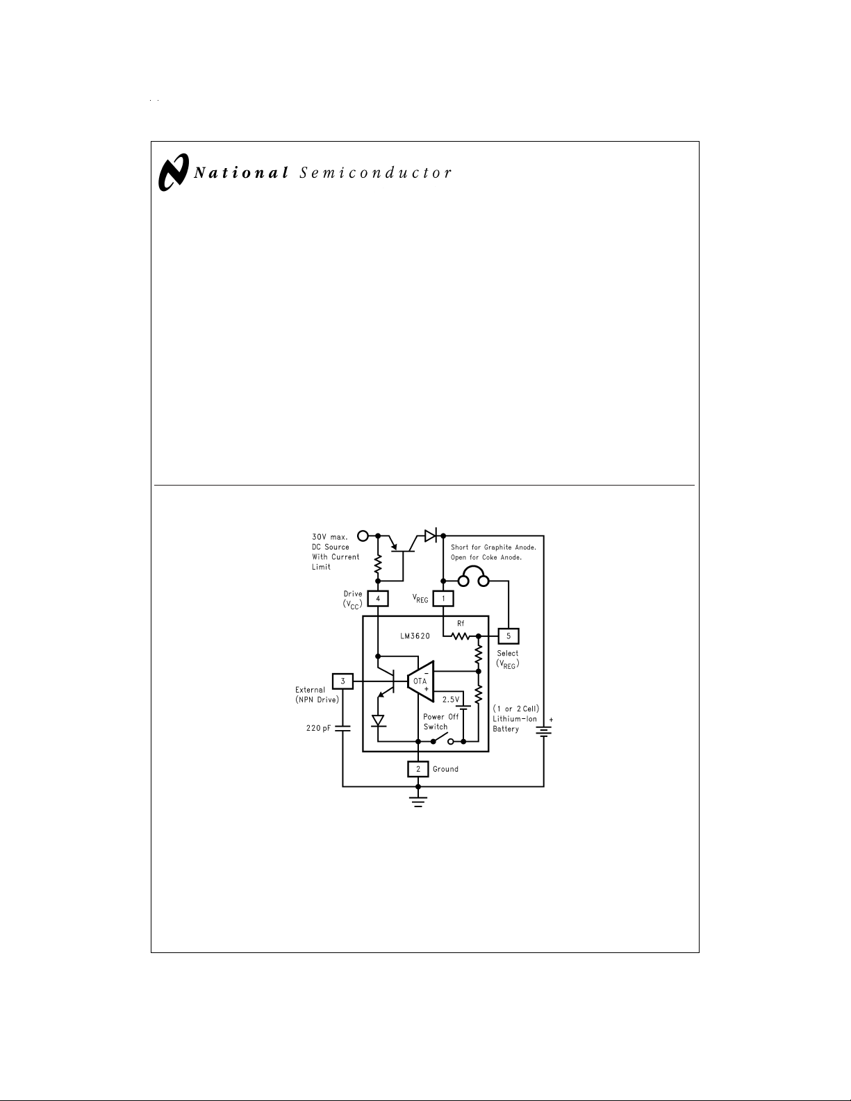
Typical Application
With a trimmed output voltage regulation of
curacy, the LM3620 provides a simple, precise solution for
end-of-charge control of lithium-ion rechargeable cells.
The LM3620 is packaged in a miniature 5-lead SOT-23 surface mount package for very compact designs.
Features
n Voltage options for charging 1 or 2 cell stacks
n Adjustable output voltage for coke or graphite anodes
n Precision end-of-charge voltage control
n Wide input voltage range (4V to 30V)
n Low off state current (
n Drive provided for external power stage
n Tiny SOT-23 package
<
10nA)
June 1999
±
1.2%initial ac-
LM3620 Lithium-Ion Battery Charger Controller
DS100841-10
© 1999 National Semiconductor Corporation DS100841 www.national.com
Page 2
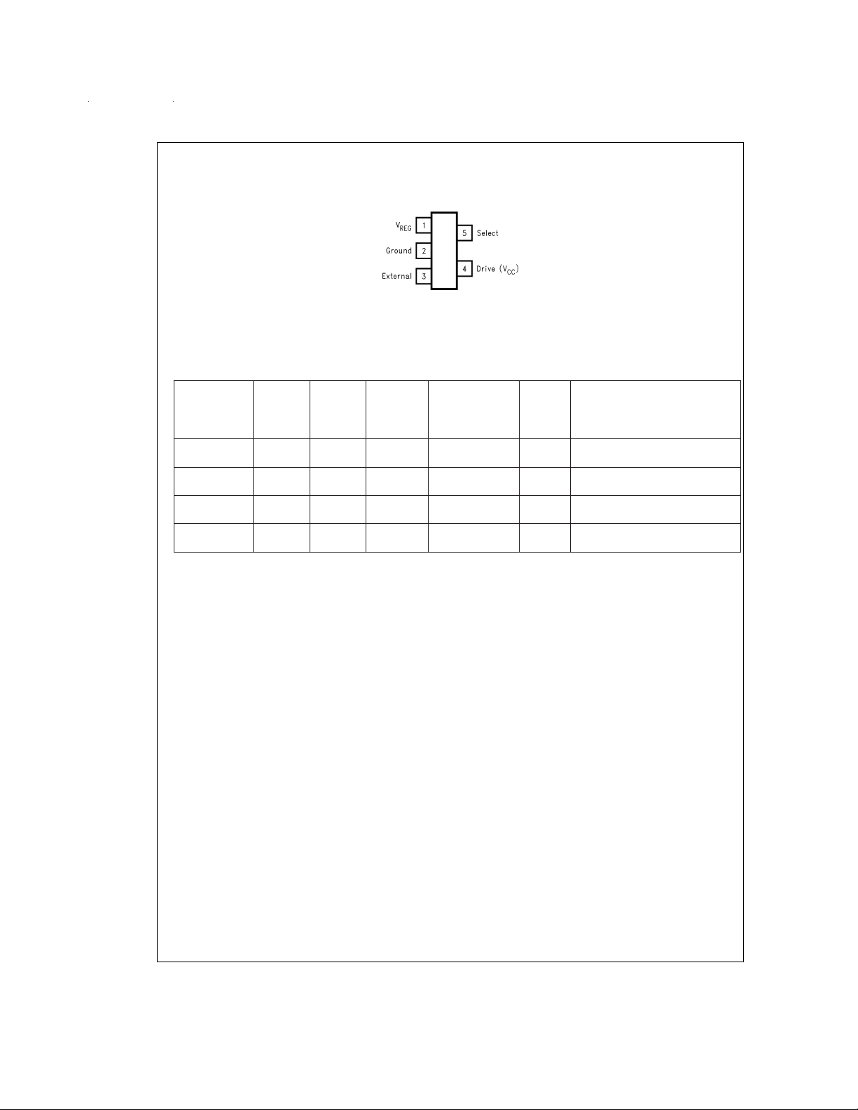
Connection Diagram
5-Lead SOT23-5 Surface Mount Package
Refer to the Ordering Information Table in
this Data Sheet for Specific Part Number
Ordering Information
Device Order
Number
LM3620M5-4 D10B 4.1V/4.2V 1.2
LM3620M5X-4 D10B 4.1V/4.2V 1.2
LM3620M5-8 D11B 8.2V/8.4V 1.2
LM3620M5X-8 D11B 8.2V/8.4V 1.2
Package
Marking
Output
Voltage
Accuracy
See NS Package MA05B
Initial
(25˚C)
%
%
%
%
Over
Temperature
Accuracy
(0 to 70˚C)
%
2
%
2
%
2
%
2
DS100841-1
Number
of Cells
1
1
2
2
Supplied as
250 Unit increments on Tape and
Reel
3k Unit increments on Tape and
Reel
250 Unit increments on Tape and
Reel
3k Unit increments on Tape and
Reel
The small physical size of the SOT23-5 Package does not allow for the full part number marking. Devices will be marked with the
designation shown in the column Package Marking.
The devices are shipped in tape-and-reel format. The standard quantity is 250 units on a reel (indicated by the letters “M5” in the
part number), or 3000 units on a reel (indicated by the letters “M5X” in the part number).
www.national.com 2
Page 3

Absolute Maximum Ratings (Note 1)
If Military/Aerospace specified devices are required,
please contact the National Semiconductor Sales Office/
Power Dissipation (T
(Note 2)
ESD Susceptibility (Note 3) 2000V
=
25˚C)
A
Distributors for availability and specifications.
Input Voltage (V
V
EXT
) 35V
DRIVE
1.5V
Junction Temperature 150˚C
Storage Temperature −65 to +150˚C
Lead Temp. Soldering
Vapor Phase (60 sec.)
Infrared (15 sec.)
215˚C
220˚C
Operating Ratings (Note 1)
Ambient Temp. Range 0˚C to 70˚C
Junction Temp. Range 0˚C to 125˚C
Thermal Resistance (Junction to
Ambient, θ
Input Voltage (V
)
J-A
) 4Vto30V
DRIVE
280˚C/W
Electrical Characteristics
LM3620-4
=
V
limits with standard typeface apply for T
DRIVE
5V, I
Symbol Parameter Conditions Typical Limit Units
V
REG
V
REG/VDRIVE
I
Q
I
OFF
I
DRIVE
Gm
(DRIVE)
I
EXT
Gm
(EXT)
R
IN
R
F
=
2mA. Limits with boldface type apply over the full operating ambient temperature range, 0˚C to +70˚C,
DRIVE
Regulated Output Voltage (pin
1 to ground)
=
25˚C.
A
Pin 5 shorted to pin 1 (graphite
anode)
4.1 4.051/4.018 V(min)
4.149/4.182 V(max)
Pin 5 open (coke anode) 4.2 4.150/4.116 V(min)
4.250/4.284 V(max)
Regulated Output Voltage
Either Pin 5 setting
±
1.2/±2.0
Tolerance
Supply Sensitivity V
Quiescent Current V
Off State Current V
Drive Pin Sink Current V
Drive Pin Transconductance ∆I
External Pin Source Current V
External Pin Transconductance ∆I
V
Input Resistance Pin 1 to Ground.
REG
for 5V ≤ V
REG
=
4.5V, V
REG
open circuited (Note 5) 10 200 nA(max)
DRIVE
=
5.0V 20 15 mA(min)
DRIVE
/∆V
DRIVE
2mA ≤ I
0mA ≤ I
REG
DRIVE
=
1V (Note 6) 3 2.5 mA(min)
EXT
/∆V
EXT
REG,VEXT
≤ 2.5mA
EXT
Circuit biased with V
open circuited
V
DRIVE
≤ 30V 100 µV/V(max)
DRIVE
=
1.0V (Note 4) 400 750 µA(max)
EXT
≤15mA
=
DRIVE
1V
applied
3 A/V
0.8 A/V
46 kΩ
42 MΩ
Feedback Resistance Pin 1 to Pin 5 1500 Ω
300mW
%
www.national.com3
Page 4

LM3620-8
=
V
limits with standard typeface apply for T
DRIVE
5V, I
Symbol Parameter Conditions Typical Limit Units
V
REG
V
REG/VDRIVE
I
Q
I
OFF
I
DRIVE
Gm
(DRIVE)
I
EXT
Gm
(EXT)
R
IN
R
F
Note 1: Absolute Maximum Ratings indicate limits beyond which damage to the device may occur. Operating Ratings indicate conditions for which the device is intended to be functional, but do not guarantee specific performance limits. For guaranteed specifications and test conditions, see the Electrical Characteristics.
Note 2: The maximum power dissipation must be derated at elevated temperatures and is limited by T
(junction-to-ambient thermal resistance) and TA(ambient temperature). The maximum power dissipation at any temperature is: PDiss
the value listed in the Absolute Maximum Ratings.
Note 3: Rating is for the human body model, a 100 pF capacitor discharged through a 1.5kΩ resistor into each pin.
Note 4: Quiescent current is all current flowing to ground when the voltage at the V
Note 5: Off current is all of the current flowing to ground including all leakage current that would be drawn from the battery connected to the V
Note 6: Whenthe External pin is being used as the driving source, it is recommended to keep the operating point of V
would bias I
DRIVE
=
2mA. Limits with boldface type apply over the full operating ambient temperature range, 0˚C to + 70˚C,
DRIVE
Regulated Output Voltage (pin
1 to ground)
=
25˚C.
A
Pin 5 shorted to pin 1 (graphite
anode)
8.2 8.102/8.036 V(min)
8.298/8.364 V(max)
Pin 5 open (coke anode) 8.4 8.299/8.232 V(min)
8.501/8.568 V(max)
Regulated Output Voltage
Either Pin 5 setting
±
1.2/±2.0
Tolerance
Supply Sensitivity V
Quiescent Current V
Off State Current V
Drive Pin Sink Current V
Drive Pin Transconductance ∆I
External Pin Source Current V
External Pin Transconductance ∆I
V
Input Resistance Pin 1 to Ground.
REG
for 5V ≤ V
REG
=
8.7V, V
REG
open circuited (Note 5) 10 200 nA(max)
DRIVE
=
5.0V 20 15 mA(min)
DRIVE
/∆V
DRIVE
2mA ≤ I
0mA ≤ I
REG
DRIVE
=
1V (Note 6) 3 2.5 mA(min)
EXT
/∆V
EXT
REG,VEXT
≤ 2.5mA
EXT
Circuit biased with V
open circuited
V
DRIVE
≤ 30V 200 µV/V(max)
DRIVE
=
1.0V (Note 4) 400 750 µA(max)
EXT
≤15mA
=
DRIVE
1V
applied
1.5 A/V
0.4 A/V
110 kΩ
42 MΩ
Feedback Resistance Pin 1 to Pin 5 2900 Ω
(maximum junction temperature), θ
JMAX
pin is forced to be above the nominal regulating voltage (V
REG
≤ 1V.Ifgreater than 1V,theinternal circuitry
to conduct up to the current limit level continuously causing unnecessary power dissipation in the device.
EXT
MAX
=
(T
JMAX−TA
REG
terminal.
REG
)/θ
J-A
).
%
up to
J-A
www.national.com 4
Page 5

Typical Performance Characteristics Unless otherwise specified, T
LM3620M5-4
Normalized Regulation Voltage
Change vs I
DRIVE
LM3620M5-4
Normalized Regulation Voltage
Change vs V
DRIVE
LM3620M5-4
Normalized Regulation Voltage
Change vs I
=
25˚C.
A
EXT
LM3620M5-4
Quiescent Current
vs V
DRIVE
LM3620M5-4
Bode Plot (∆V
DRIVE
/∆V
REG
DS100841-4
DS100841-5
)
LM3620M5-4
Off State Current vs V
DRIVE
DS100841-8
DS100841-6
DS100841-7
LM3620M5-4
Off State Current
vs Temperature
DS100841-3
DS100841-9
www.national.com5
Page 6

Physical Dimensions inches (millimeters) unless otherwise noted
LM3620 Lithium-Ion Battery Charger Controller
SOT23-5 Package
5-Lead Small-Outline Package (M5)
For Ordering, Refer to Ordering Information Table
NS Package Number MA05B
LIFE SUPPORT POLICY
NATIONAL’S PRODUCTS ARE NOT AUTHORIZED FOR USE AS CRITICAL COMPONENTS IN LIFE SUPPORT
DEVICES OR SYSTEMS WITHOUT THE EXPRESS WRITTEN APPROVAL OF THE PRESIDENT AND GENERAL
COUNSEL OF NATIONAL SEMICONDUCTOR CORPORATION. As used herein:
1. Life support devices or systems are devices or
systems which, (a) are intended for surgical implant
into the body, or (b) support or sustain life, and
whose failure to perform when properly used in
accordance with instructions for use provided in the
2. A critical component is any component of a life
support device or system whose failure to perform
can be reasonably expected to cause the failure of
the life support device or system, or to affect its
safety or effectiveness.
labeling, can be reasonably expected to result in a
significant injury to the user.
National Semiconductor
Corporation
Americas
Tel: 1-800-272-9959
Fax: 1-800-737-7018
Email: support@nsc.com
www.national.com
National does not assume any responsibility for use of any circuitry described, no circuit patent licenses are implied and National reserves the right at any time without notice to change said circuitry and specifications.
National Semiconductor
Europe
Fax: +49 (0) 1 80-530 85 86
Email: europe.support@nsc.com
Deutsch Tel: +49 (0) 1 80-530 85 85
English Tel: +49 (0) 1 80-532 78 32
Français Tel: +49 (0) 1 80-532 93 58
Italiano Tel: +49 (0) 1 80-534 16 80
National Semiconductor
Asia Pacific Customer
Response Group
Tel: 65-2544466
Fax: 65-2504466
Email: sea.support@nsc.com
National Semiconductor
Japan Ltd.
Tel: 81-3-5639-7560
Fax: 81-3-5639-7507
 Loading...