

Page 1

LM160/LM360
High Speed Differential Comparator
General Description
The LM160/LM360 is a very high speed differential input,
complementary TTL output voltage comparator with improved characteristics over the µA760/µA760C, for which it
is a pin-for-pin replacement. The device has been optimized
for greater speed, input impedance and fan-out, and lower
input offset voltage. Typicallydelay varies only 3 ns for overdrive variations of 5 mV to 400 mV.
Complementary outputs having minimum skew are provided.
Applications involve high speed analog to digital convertors
and zero-crossing detectors in disk file systems.
Features
n Guaranteed high speed: 20 ns max
n Tight delay matching on both outputs
n Complementary TTL outputs
n High input impedance
n Low speed variation with overdrive variation
n Fan-out of 4
n Low input offset voltage
n Series 74 TTL compatible
Connection Diagrams
Metal Can Package
DS005707-4
Order Number LM160H/883 (Note 1) or LM360H
See NS Package Number H08C
Dual-In-Line Package
DS005707-5
Order Number LM360M or LM360N
See NS Package Number M08A or N08E
Note 1: Also available in SMD#5962-8767401
May 1999
LM160/LM360 High Speed Differential Comparator
© 1999 National Semiconductor Corporation DS005707 www.national.com
Page 2

Absolute Maximum Ratings (Notes 6, 8)
If Military/Aerospace specified devices are required,
please contact the National Semiconductor Sales Office/
Distributors for availability and specifications.
Positive Supply Voltage +8V
Negative Supply Voltage −8V
Peak Output Current 20 mA
Differential Input Voltage
±
5V
Input Voltage V
+
≥ VIN≥ V
−
ESD Tolerance (Note 9) 1600V
Operating Temperature Range
LM160 −55˚C to +125˚C
LM360 0˚C to +70˚C
Storage Temperature Range −65˚C to +150˚C
Lead Temperature
(Soldering, 10 sec.) 260˚C
Soldering Information
Dual-In-Line Package
Soldering (10 seconds) 260˚C
Small Outline Package
Vapor Phase (60 seconds) 215˚C
Infrared (15 seconds) 220˚C
See AN-450 “Surface Mounting Methods and Their Effect
on Product Reliability” for other methods of soldering
surface mount devices.
Electrical Characteristics
(T
MIN
≤ TA≤ T
MAX
)
Parameter Conditions Min Typ Max Units
Operating Conditions
Supply Voltage V
CC
+
4.5 5 6.5 V
Supply Voltage V
CC
−
−4.5 −5 −6.5 V
Input Offset Voltage R
S
≤ 200Ω 25mV
Input Offset Current 0.5 3 µA
Input Bias Current 520µA
Output Resistance (Either Output) V
OUT
=
V
OH
100 Ω
Response Time T
A
=
25˚C, V
S
=
±
5V (Notes 2, 7) 13 25 ns
T
A
=
25˚C, V
S
=
±
5V (Notes 3, 7) 12 20 ns
T
A
=
25˚C, V
S
=
±
5V (Notes 4, 7) 14 ns
Response Time Difference between Outputs
(t
pd
of +V
IN1
)−(tpdof −V
IN2
)T
A
=
25˚C (Notes 2, 7) 2 ns
(t
pd
of +V
IN2
)−(tpdof −V
IN1
)T
A
=
25˚C (Notes 2, 7) 2 ns
(t
pd
of +V
IN1
)−(tpdof +V
IN2
)T
A
=
25˚C (Notes 2, 7) 2 ns
(t
pd
of −V
IN1
)−(tpdof −V
IN2
)T
A
=
25˚C (Notes 2, 7) 2 ns
Input Resistance f=1 MHz 17 kΩ
Input Capacitance f=1 MHz 3 pF
Average Temperature Coefficient of R
S
=
50Ω 8 µV/˚C
Input Offset Voltage
Average Temperature Coefficient of 7 nA/˚C
Input Offset Current
Common Mode Input Voltage Range V
S
=
±
6.5V
±
4
±
4.5 V
Differential Input Voltage Range
±
5V
Output High Voltage (Either Output) I
OUT
=
−320 µA, V
S
=
±
4.5V 2.4 3 V
Output Low Voltage (Either Output) I
SINK
=
6.4 mA 0.25 0.4 V
Positive Supply Current V
S
=
±
6.5V 18 32 mA
Negative Supply Current V
S
=
±
6.5V −9 −16 mA
Note 2: Response time measured from the 50%point of a 30 mVp-p 10 MHz sinusoidal input to the 50%point of the output.
Note 3: Response time measured from the 50%point of a 2 Vp-p 10 MHz sinusoidal input to the 50%point of the output.
Note 4: Response time measured from the start of a 100 mV input step with 5 mV overdrive to the time when the output crosses the logic threshold.
Note 5: Typical thermal impedances are as follows:
Cavity DIP (J): θ
jA
135˚C/W Header (H) θ
jA
165˚C/W (Still Air)
Molded DIP (N): θ
jA
130˚C/W 67˚C/W (400LF/min Air Flow)
θ
jC
25˚C/W
Note 6: The device may be damaged if used beyond the maximum ratings.
Note 7: Measurements are made in AC Test Circuit, Fanout=1
Note 8: Refer to RETS 160X for LM160H, LM160J-14 and LM160J military specifications.
www.national.com 2
Page 3
Electrical Characteristics (Continued)
Note 9: Human body model, 1.5 kΩ in series with 100 pF.
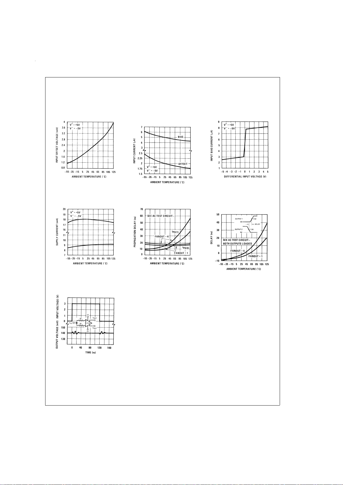
Typical Performance Characteristics
Offset Voltage
DS005707-8
Input Current vs Ambient
Temperature
DS005707-9
Input Characteristics
DS005707-10
Supply Current vs Ambient
Temperature
DS005707-11
Propagation Delay vs
Ambient Temperature
DS005707-12
Delay of Output 1 With
Respect to Output 2 vs
Ambient Temperature
DS005707-13
Common-Mode
Pulse Response
DS005707-14
www.national.com3
Page 4

AC Test Circuit
DS005707-3
V
IN
=
±
50 mV FANOUT=1 FANOUT=4
V
+
=
+5V R=2.4k R=630Ω
V
−
=
−5V C=15 pF C=30 pF
www.national.com 4
Page 5

Schematic Diagram
DS005707-1
www.national.com5
Page 6

Physical Dimensions inches (millimeters) unless otherwise noted
Metal Can Package (H)
Order Number LM160H/883 or LM360H
NS Package Number H08C
Molded Dual-In-Line Package (M)
Order Number LM360M
NS Package Number M08A
www.national.com 6
Page 7

Physical Dimensions inches (millimeters) unless otherwise noted (Continued)
LIFE SUPPORT POLICY
NATIONAL’S PRODUCTS ARE NOT AUTHORIZED FOR USE AS CRITICAL COMPONENTS IN LIFE SUPPORT
DEVICES OR SYSTEMS WITHOUT THE EXPRESS WRITTEN APPROVAL OF THE PRESIDENT AND GENERAL
COUNSEL OF NATIONAL SEMICONDUCTOR CORPORATION. As used herein:
1. Life support devices or systems are devices or
systems which, (a) are intended for surgical implant
into the body, or (b) support or sustain life, and
whose failure to perform when properly used in
accordance with instructions for use provided in the
labeling, can be reasonably expected to result in a
significant injury to the user.
2. A critical component is any component of a life
support device or system whose failure to perform
can be reasonably expected to cause the failure of
the life support device or system, or to affect its
safety or effectiveness.
National Semiconductor
Corporation
Americas
Tel: 1-800-272-9959
Fax: 1-800-737-7018
Email: support@nsc.com
National Semiconductor
Europe
Fax: +49 (0) 1 80-530 85 86
Email: europe.support@nsc.com
Deutsch Tel: +49 (0) 1 80-530 85 85
English Tel: +49 (0) 1 80-532 78 32
Français Tel: +49 (0) 1 80-532 93 58
Italiano Tel: +49 (0) 1 80-534 16 80
National Semiconductor
Asia Pacific Customer
Response Group
Tel: 65-2544466
Fax: 65-2504466
Email: sea.support@nsc.com
National Semiconductor
Japan Ltd.
Tel: 81-3-5639-7560
Fax: 81-3-5639-7507
www.national.com
Molded Dual-In-Line Package (N)
Order Number LM360N
NS Package Number N08E
LM160/LM360 High Speed Differential Comparator
National does not assume any responsibility for use of any circuitry described, no circuit patent licenses are implied and National reserves the right at any time without notice to change said circuitry and specifications.
 Loading...