

Page 1
LM359
Dual, High Speed, Programmable, Current Mode (Norton)
Amplifiers
General Description
The LM359 consists of two current differencing (Norton) input amplifiers. Design emphasis has been placed on obtaining high frequency performance and providing user programmable amplifier operating characteristics. Each amplifier is
broadbanded to provide a high gain bandwidth product, fast
slew rate and stable operation for an inverting closed loop
gain of 10 or greater. Pins for additional external frequency
compensation are provided. The amplifiers are designed to
operate from a single supply and can accommodate input
common-mode voltages greater than the supply.
Applications
n General purpose video amplifiers
n High frequency, high Q active filters
n Photo-diode amplifiers
n Wide frequency range waveform generation circuits
n All LM3900 AC applications work to much higher
frequencies
Features
n User programmable gain bandwidth product, slew rate,
input bias current, output stage biasing current and total
device power dissipation
n High gain bandwidth product (I
SET
=
0.5 mA)
400 MHz for A
V
=
10 to 100
30 MHz for A
V
=
1
n High slew rate (I
SET
=
0.5 mA)
60 V/µs for A
V
=
10 to 100
30 V/µs for A
V
=
1
n Current differencing inputs allow high common-mode
input voltages
n Operates from a single 5V to 22V supply
n Large inverting amplifier output swing, 2 mV to V
CC
−
2V
n Low spot noise,
for f>1 kHz
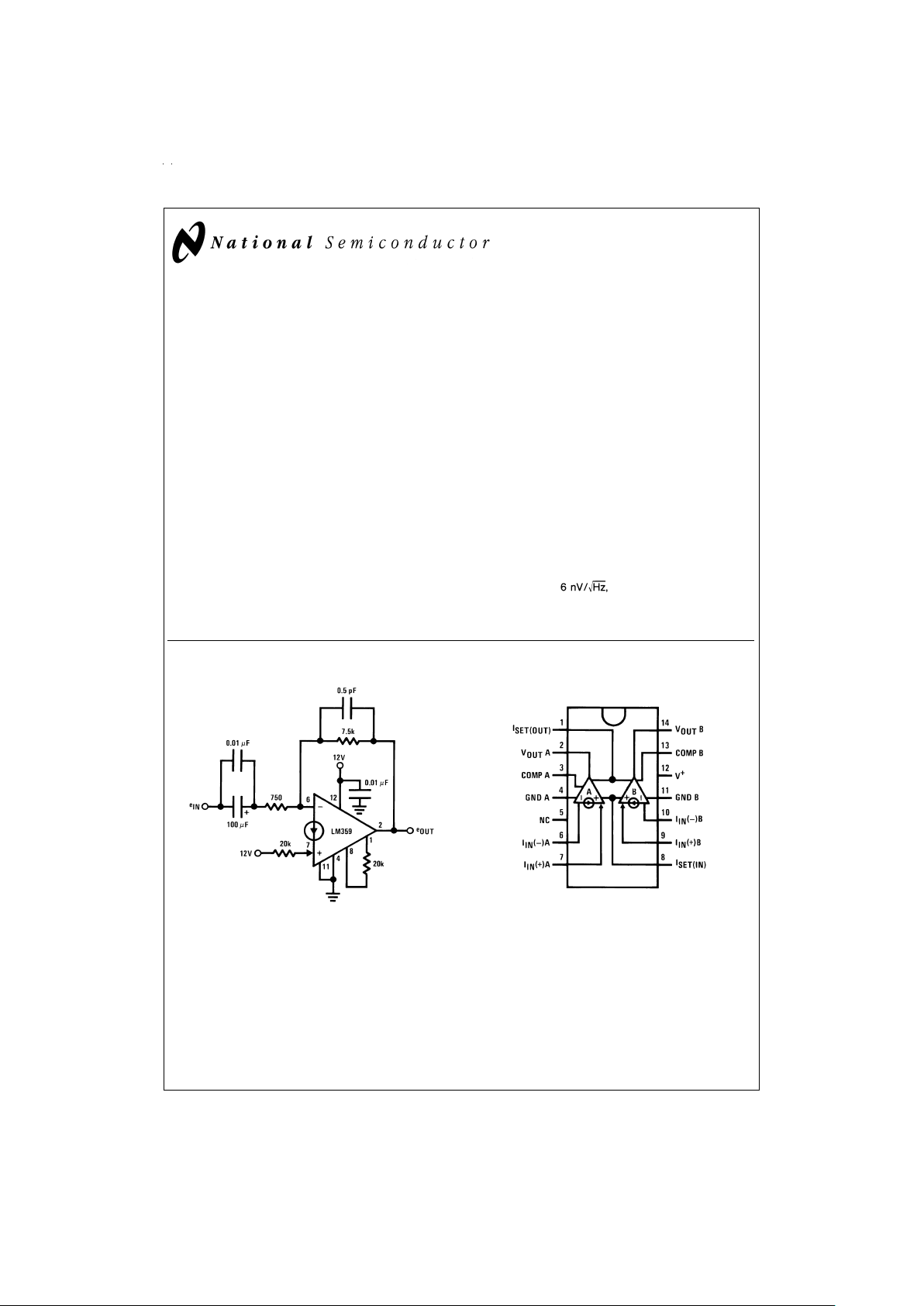
Typical Application Connection Diagram
DS007788-1
•
A
V
=
20 dB
•
−3 dB bandwidth=2.5 Hz to 25 MHz
•
Differential phase error<1˚ at 3.58 MHz
•
Differential gain error<0.5%at 3.58 MHz
Dual-In-Line Package
DS007788-2
Top View
Order Number LM359J, LM359M or LM359N
See NS Package Number J14A, M14A or N14A
October 1998
LM359 Dual, High Speed, Programmable, Current Mode (Norton) Amplifiers
© 1999 National Semiconductor Corporation DS007788 www.national.com
Page 2
Absolute Maximum Ratings (Note 1)
If Military/Aerospace specified devices are required,
please contact the National Semiconductor Sales Office/
Distributors for availability and specifications.
Supply Voltage 22 V
DC
or±11 V
DC
Power Dissipation (Note 2)
J Package 1W
N Package 750 mW
Maximum T
J
J Package +150˚C
N Package +125˚C
Thermal Resistance
J Package
θ
jA
147˚C/W still air
110˚C/W with 400 linear feet/min air flow
N Package
θ
jA
100˚C/W still air
75˚C/W with 400 linear feet/min air flow
Input Currents, I
IN
(+) or IIN(−) 10 mA
DC
Set Currents, I
SET(IN)
or I
SET(OUT)
2mA
DC
Operating Temperature Range
LM359 0˚C to +70˚C
Storage Temperature Range −65˚C to +150˚C
Lead Temperature
(Soldering, 10 sec.) 260˚C
Soldering Information
Dual-In-Line Package
Soldering (10 sec.) 260˚C
Small Outline Package
Vapor Phase (60 sec.) 215˚C
Infrared (15 sec.) 220˚C
See AN-450 “Surface Mounting Methods and Their Effect
on Product Reliability” for other methods of soldering
surface mount devices.
ESD rating to be determined.
Electrical Characteristics
I
SET(IN)
=
I
SET(OUT)
=
0.5 mA, V
supply
=
12V, T
A
=
25˚C unless otherwise noted
Parameter Conditions LM359 Units
Min Typ Max
Open Loop Voltage V
supply
=
12V, R
L
=
1k, f=100 Hz 62 72 dB
Gain T
A
=
125˚C 68 dB
Bandwidth R
IN
=
1kΩ,C
comp
=
10 pF 15 30 MHz
Unity Gain
Gain Bandwidth Product R
IN
=
50Ω to 200Ω 200 400 MHz
Gain of 10 to 100
Slew Rate
Unity Gain R
IN
=
1kΩ,C
comp
=
10 pF 30 V/µs
Gain of 10 to 100 R
IN
<
200Ω 60 V/µs
Amplifier to Amplifier f=100 Hz to 100 kHz, R
L
=
1k −80 dB
Coupling
Mirror Gain at 2 mA I
IN
(+), I
SET
=
5 µA, T
A
=
25˚C 0.9 1.0 1.1 µA/µA
(Note 3) at 0.2 mA I
IN
(+), I
SET
=
5 µA 0.9 1.0 1.1 µA/µA
Over Temp.
at 20 µA I
IN
(+), I
SET
=
5 µA 0.9 1.0 1.1 µA/µA
Over Temp.
∆Mirror Gain at 20 µA to 0.2 mA I
IN
(+) 3 5
%
(Note 3) Over Temp, I
SET
=
5µA
Input Bias Current Inverting Input, T
A
=
25˚C 8 15 µA
Over Temp. 30 µA
Input Resistance (βre) Inverting Input 2.5 kΩ
Output Resistance I
OUT
=
15 mA rms, f=1 MHz 3.5 Ω
Output Voltage Swing R
L
=
600Ω
V
OUT
High IIN(−) and IIN(+) Grounded 9.5 10.3 V
V
OUT
Low IIN(−)=100 µA, IIN(+)=0 2 50 mV
www.national.com 2
Page 3
Electrical Characteristics (Continued)
I
SET(IN)
=
I
SET(OUT)
=
0.5 mA, V
supply
=
12V, T
A
=
25˚C unless otherwise noted
Parameter Conditions LM359 Units
Min Typ Max
Output Currents
Source I
IN
(−) and IIN(+) Grounded, R
L
=
100Ω 16 40 mA
Sink (Linear Region) V
comp
−0.5V=V
OUT
=
1V, I
IN
(+)=0 4.7 mA
Sink (Overdriven) I
IN
(−)=100 µA, IIN(+)=0, 1.5 3 mA
V
OUT
Force=1V
Supply Current Non-Inverting Input 18.5 22 mA
Grounded, R
L
=
∞
Power Supply Rejection f=120 Hz, IIN(+) Grounded 40 50 dB
(Note 4)
Note 1: “Absolute Maximum Ratings” indicate limits beyond which damage to the device may occur. Operating Ratings indicate conditions for which the device is
functional, but do not guarantee specific performance limits.
Note 2: See Maximum Power Dissipation graph.
Note 3: Mirror gain is the current gain of the current mirror which is used as the non-inverting input.
∆Mirror Gain is the%change in AIfor two different mirror currents at any given temperature.
Note 4: See Supply Rejection graphs.
www.national.com3
Page 4
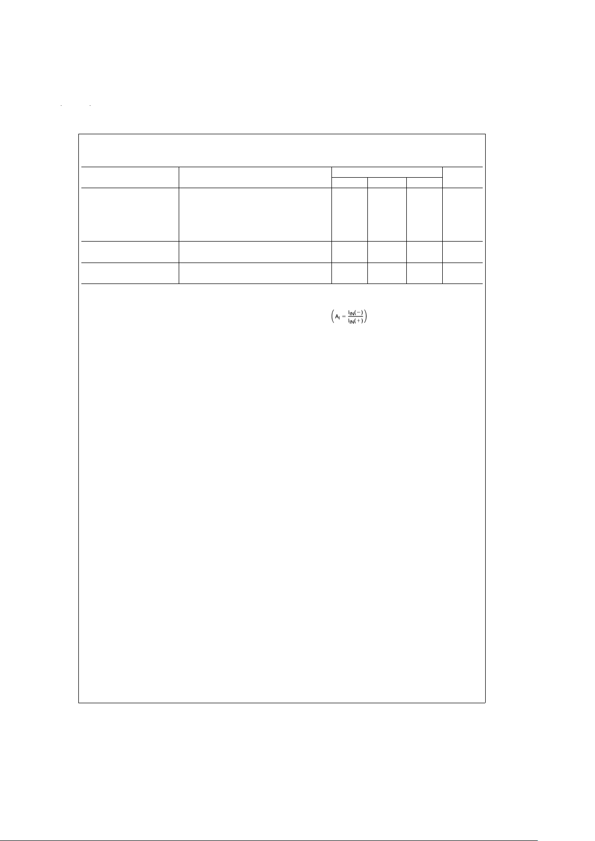
Schematic Diagram
DS007788-3
www.national.com 4
Page 5
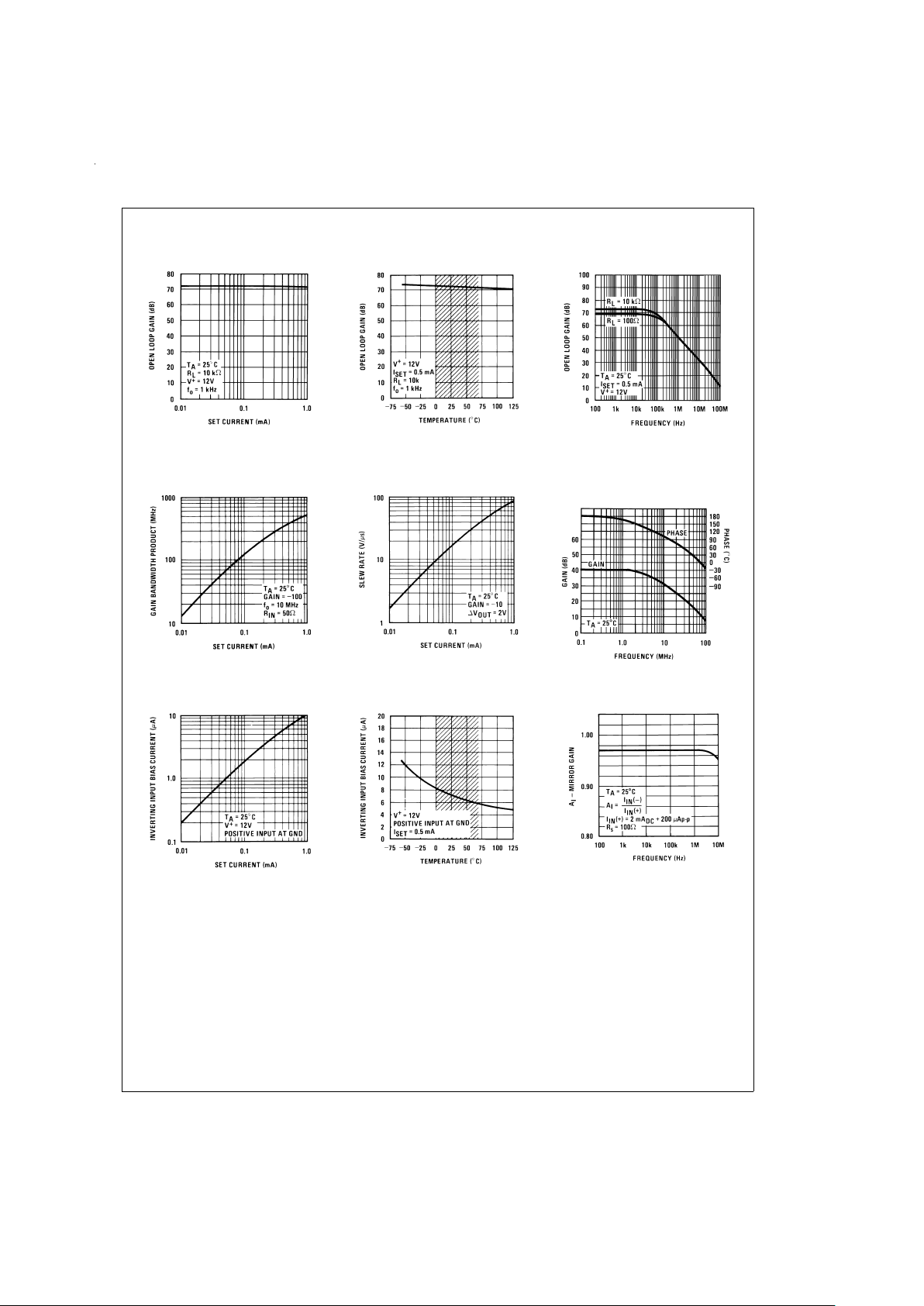
Typical Performance Characteristics
Open Loop Gain
DS007788-39
Open Loop Gain
DS007788-40
Note: Shaded area refers to LM359
Open Loop Gain
DS007788-41
Gain Bandwidth Product
DS007788-42
Slew Rate
DS007788-43
Gain and Phase
Feedback Gain=− 100
DS007788-44
Inverting Input Bias Current
DS007788-45
Inverting Input Bias Current
DS007788-46
Note: Shaded area refers to LM359
Mirror Gain
DS007788-47
www.national.com5
Page 6
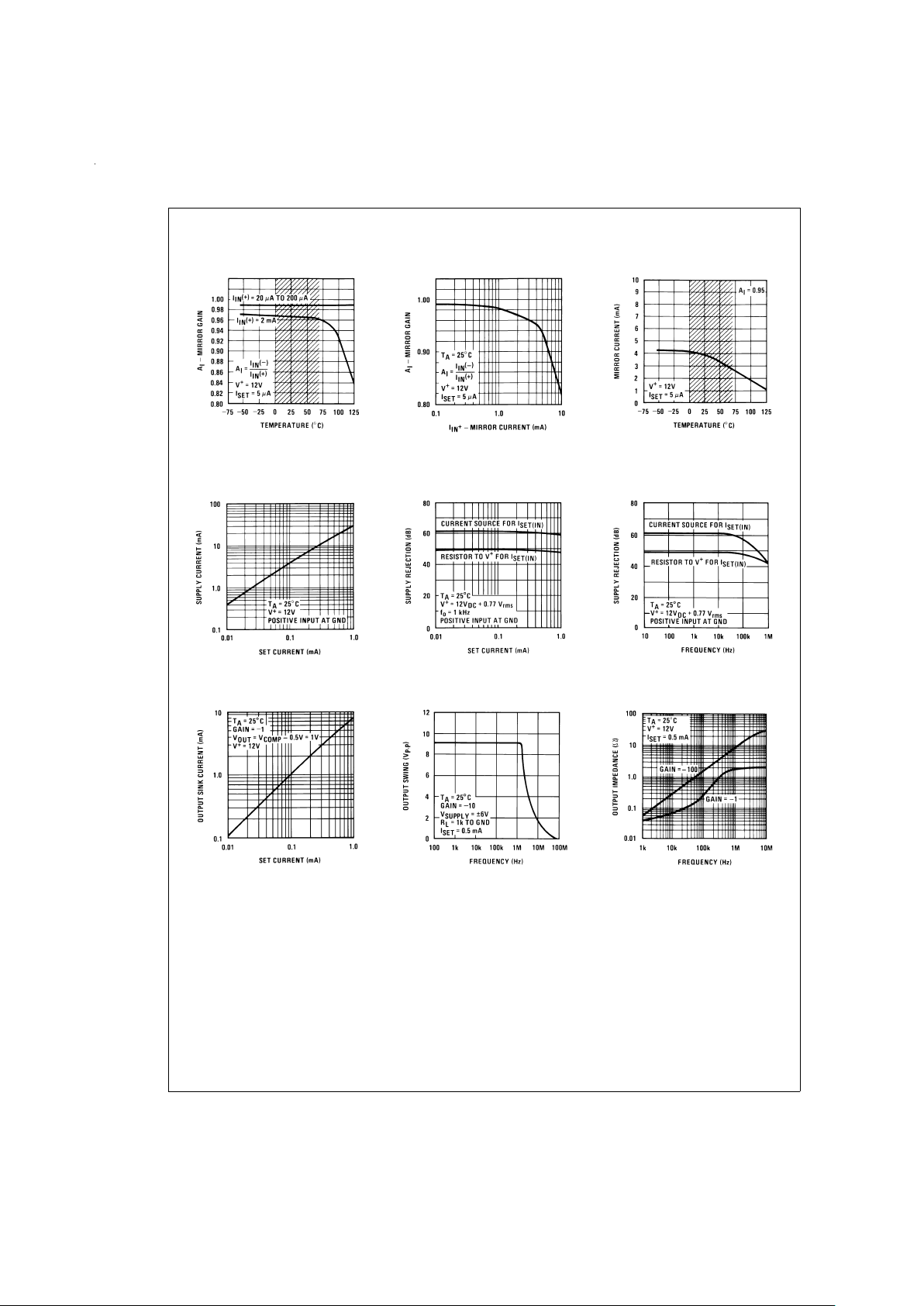
Typical Performance Characteristics (Continued)
Mirror Gain
DS007788-48
Note: Shaded area refers to LM359
Mirror Gain
DS007788-49
Mirror Current
DS007788-50
Note: Shaded area refers to LM359
Supply Current
DS007788-51
Supply Rejection
DS007788-52
Supply Rejection
DS007788-53
Output Sink Current
DS007788-54
Output Swing
DS007788-55
Output Impedance
DS007788-56
www.national.com 6
Page 7
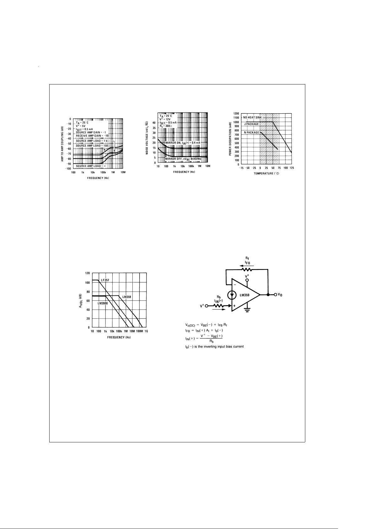
Typical Performance Characteristics (Continued)
Application Hints
The LM359 consists of two wide bandwidth, decompensated
current differencing (Norton) amplifiers. Although similar in
operation to the original LM3900, design emphasis for these
amplifiers has been placed on obtaining much higher frequency performance as illustrated in
Figure 1
.
This significant improvement in frequency response is the
result of using a common-emitter/common-base (cascode)
gain stage which is typical in many discrete and integrated
video and RF circuit designs. Another versatile aspect of
these amplifiers is the ability to externally program many internal amplifier parameters to suit the requirements of a wide
variety of applications in which this type of amplifier can be
used.
DC BIASING
The LM359 is intended for single supply voltage operation
which requires DC biasing of the output. The current mirror
circuitry which provides the non-inverting input for the amplifier also facilitates DC biasing the output. The basic operation of this current mirror is that
the current (both DC and AC)
flowing into the non-inverting input will force an equal
amount of current to flow into the inverting input
. The mirror
gain (A
I
) specification is the measure of how closely these
two currents match. For more details see National Application Note AN-72.
DC biasing of the output is accomplished by establishing a
reference DC current into the (+) input, I
IN
(+), and requiring
the output to provide the (−) input current. This forces the
output DC level to be whatever value necessary (within the
output voltage swing of the amplifier) to provide this DC reference current,
Figure 2
.
The DC input voltage at each input is a transistor V
BE
(≅0.6 VDC) and must be considered for DC biasing. For
most applications, the supply voltage, V
+
, is suitable and
convenient for establishing I
IN
(+). The inverting input bias
current, I
b
(−), is a direct function of the programmable input
stage current (see current programmability section) and to
obtain predictable output DC biasing set I
IN
(+) ≥ 10Ib(−).
Amplifier to Amplifier
Coupling (Input Referred)
DS007788-57
Noise Voltage
DS007788-58
Maximum Power Dissipation
DS007788-59
Note: Shaded area refers to LM359J/LM359N
DS007788-6
FIGURE 1.
DS007788-7
FIGURE 2.
www.national.com7
Page 8
Application Hints (Continued)
The following figures illustrate typical biasing schemes for
AC amplifiers using the LM359:
The nV
BE
biasing configuration is most useful for low noise
applications where a reduced input impedance can be accommodated (see typical applications section).
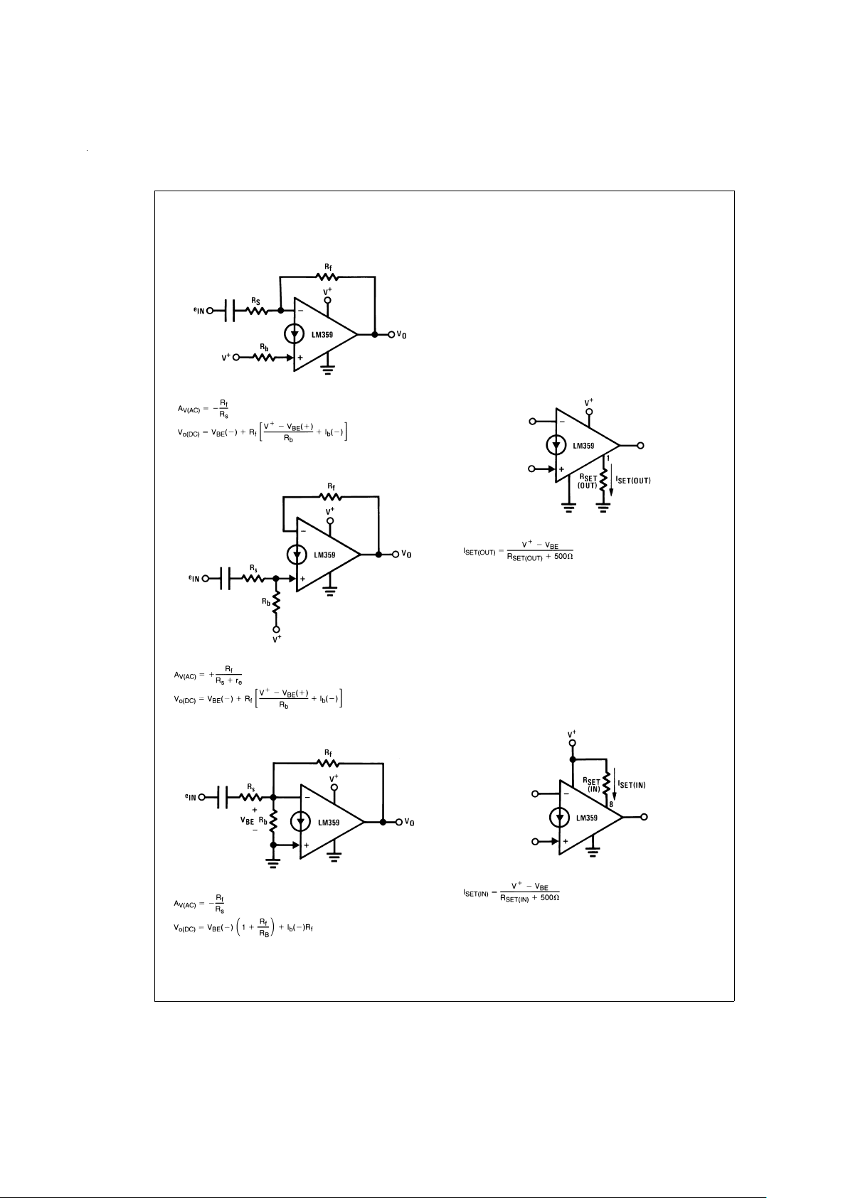
OPERATING CURRENT PROGRAMMABILITY (I
SET
)
The input bias current, slew rate, gain bandwidth product,
output drive capability and total device power consumption
of both amplifiers can be simultaneously controlled and optimized via the two programming pins I
SET(OUT)
and I
SET(IN)
.
I
SET(OUT)
The output set current (I
SET(OUT)
) is equal to the amount of
current sourced from pin 1 and establishes the class A biasing current for the Darlington emitter follower output stage.
Using a single resistor from pin 1 to ground, as shown in
Fig-
ure 6
, this current is equal to:
The output set current can be adjusted to optimize the
amount of current the output of the amplifier can sink to drive
load capacitance and for loads connected to V
+
.
The maximum output sinking current is approximately 10 times
I
SET(OUT)
. This set current is best used to reduce the total
device supply current if the amplifiers are not required to
drive small load impedances.
I
SET(IN)
The input set current I
SET(IN)
is equal to the current flowing
into pin 8. A resistor from pin 8 to V
+
sets this current to be:
I
SET(IN)
is most significant in controlling the AC characteristics of the LM359 as it directly sets the total input stage current of the amplifiers which determines the maximum slew
rate, the frequency of the open loop dominant pole, the input
resistance of the (−) input and the biasing current I
b
(−).All of
DS007788-8
FIGURE 3. Biasing an Inverting AC Amplifier
DS007788-9
FIGURE 4. Biasing a Non-Inverting AC Amplifier
DS007788-10
FIGURE 5. nVBEBiasing
DS007788-11
FIGURE 6. Establishing the Output Set Current
DS007788-12
FIGURE 7. Establishing the Input Set Current
www.national.com 8
Page 9

Application Hints (Continued)
these parameters are significant in wide band amplifier design. The input stage current is approximately 3 times
I
SET(IN)
and by using this relationship the following first order
approximations for these AC parameters are:
where C
comp
is the total capacitance from the compensation
pin (pin 3 or pin 13) to ground, A
VOL
is the low frequency
open loop voltage gain in V/V and an ambient temperature of
25˚C is assumed (KT/q=26 mV and β
typ
=
150). I
SET(IN)
also controls the DC input bias current by the expression:
which is important for DC biasing considerations.
The total device supply current (for both amplifiers) is also a
direct function of the set currents and can be approximated
by:
I
supply
≅
27xI
SET(OUT)
+11xI
SET(IN)
with each set current programmed by individual resistors.
PROGRAMMING WITH A SINGLE RESISTOR
Operating current programming may also be accomplished
using only one resistor by letting I
SET(IN)
equal I
SET(OUT)
. The
programming current is now referred to as I
SET
and it is cre-
ated by connecting a resistor from pin 1 to pin 8 (
Figure 8
).
This configuration does not affect any of the internal set current dependent parameters differently than previously discussed except the total supply current which is now equal to:
I
supply
≅
37xI
SET
Care must be taken when using resistors to program the set
current to prevent significantly increasing the supply voltage
above the value used to determine the set current. This
would cause an increase in total supply current due to the resulting increase in set current and the maximum device
power dissipation could be exceeded. The set resistor value(s) should be adjusted for the new supply voltage.
One method to avoid this is to use an adjustable current
source which has voltage compliance to generate the set
current as shown in
Figure 9
.
This circuit allows I
SET
to remain constant over the entire
supply voltage range of the LM359 which also improves
power supply ripple rejection as illustrated in the Typical Performance Characteristics. It should be noted, however, that
the current through the LM334 as shown will change linearly
with temperature but this can be compensated for (see
LM334 data sheet).
Pin 1 must never be shorted to ground or pin 8 never shorted
to V
+
without limiting the current to 2 mA or less to prevent
catastrophic device failure.
CONSIDERATIONS FOR HIGH FREQUENCY
OPERATION
The LM359 is intended for use in relatively high frequency
applications and many factors external to the amplifier itself
must be considered. Minimization of stray capacitances and
their effect on circuit operation are the primary requirements.
The following list contains some general guidelines to help
accomplish this end:
1. Keep the leads of all external components as short as
possible.
2. Place components conducting signal current from the
output of an amplifier away from that amplifier’s
non-inverting input.
3. Use reasonably low value resistances for gain setting
and biasing.
4. Use of a ground plane is helpful in providing a shielding
effect between the inputs and from input to output.Avoid
using vector boards.
5. Use a single-point ground and single-point supply distri-
bution to minimize crosstalk. Always connect the two
grounds (one from each amplifier) together.
6. Avoid use of long wires (
>
2") but if necessary, use
shielded wire.
7. Bypass the supply close to the device with a low induc-
tance, low value capacitor (typically a 0.01 µF ceramic)
to create a good high frequency ground. If long supply
leads are unavoidable, a small resistor (
z
10Ω) in series
with the bypass capacitor may be needed and using
shielded wire for the supply leads is also recommended.
COMPENSATION
The LM359 is internally compensated for stability with closed
loop inverting gains of 10 or more. For an inverting gain of
less than 10 and all non-inverting amplifiers (the amplifier always has 100%negative current feedback regardless of the
DS007788-13
I
SET(IN)
=
I
SET(OUT)
=
I
SET
FIGURE 8. Single Resistor Programming of I
SET
DS007788-14
FIGURE 9. Current Source Programming of I
SET
www.national.com9
Page 10

Application Hints (Continued)
gain in the non-inverting configuration) some external frequency compensation is required because the stray capacitance to ground from the (−) input and the feedback resistor
add additional lagging phase within the feedback loop. The
value of the input capacitance will typically be in the range of
6 pF to 10 pF for a reasonably constructed circuit board.
When using a feedback resistance of 30 kΩ or less, the best
method of compensation, without sacrificing slew rate, is to
add a lead capacitor in parallel with the feedback resistor
with a value on the order of 1 pF to 5 pF as shown in
Figure
10
.
Another method of compensation is to increase the effective
value of the internal compensation capacitor by adding capacitance from the COMP pin of an amplifier to ground. An
external 20 pF capacitor will generally compensate for all
gain settings but will also reduce the gain bandwidth product
and the slew rate. These same results can also be obtained
by reducing I
SET(IN)
if the full capabilities of the amplifier are
not required. This method is termed over-compensation.
Another area of concern from a stability standpoint is that of
capacitive loading. The amplifier will generally drive capacitive loads up to 100 pF without oscillation problems. Any
larger C loads can be isolated from the output as shown in
Figure 11
. Over-compensation of the amplifier can also be
used if the corresponding reduction of the GBW product can
be afforded.
In most applications using the LM359, the input signal will be
AC coupled so as not to affect the DC biasing of the amplifier. This gives rise to another subtlety of high frequency cir-
cuits which is the effective series inductance (ESL) of the
coupling capacitor which creates an increase in the impedance of the capacitor at high frequencies and can cause an
unexpected gain reduction. Low ESL capacitors like solid
tantalum for large values of C and ceramic for smaller values
are recommended. A parallel combination of the two types is
even better for gain accuracy over a wide frequency range.
AMPLIFIER DESIGN EXAMPLES
The ability of the LM359 to provide gain at frequencies
higher than most monolithic amplifiers can provide makes it
most useful as a basic broadband amplification stage. The
design of standard inverting and non-inverting amplifiers,
though different than standard op amp design due to the current differencing inputs, also entail subtle design differences
between the two types of amplifiers. These differences will
be best illustrated by design examples. For these examples
a practical video amplifier with a passband of 8 Hz to 10 MHz
and a gain of 20 dB will be used. It will be assumed that the
input will come from a 75Ω source and proper signal termination will be considered. The supply voltage is 12 V
DC
and
single resistor programming of the operating current, I
SET
,
will be used for simplicity.
AN INVERTING VIDEO AMPLIFIER
1. Basic circuit configuration:
2. Determine the required I
SET
from the characteristic
curves for gain bandwidth product.
GBW
MIN
=
10x10MHz=100 MHz
For a flat response to 10 MHz a closed loop response to two
octaves above 10 MHz (40 MHz) will be sufficient.
Actual GBW=10x40MHz=400 MHz
I
SET
required=0.5 mA
DS007788-15
C
f
=
1 pF to 5 pF for stability
FIGURE 10. Best Method of Compensation
DS007788-16
FIGURE 11. Isolating Large Capacitive Loads
DS007788-17
www.national.com 10
Page 11

Application Hints (Continued)
3. Determine maximum value for R
f
to provide stable DC
biasing
Optimum output DC level for maximum symmetrical swing
without clipping is:
R
f(MAX)
can now be found:
This value should not be exceeded for predictable DC biasing.
4. Select R
s
to be large enough so as not to appreciably
load the input termination resistance:
R
s
≥ 750Ω; Let R
s
=
750Ω
5. Select R
f
for appropriate gain:
7.5 kΩ is less than the calculated R
f(MAX)
so DC predictability
is insured.
6. Since R
f
=
7.5k, for the output to be biased to 5.1 V
DC
,
the reference current I
IN
(+) must be:
Now Rbcan be found by:
7. Select Cito provide the proper gain for the 8 Hz minimum input frequency:
Alarger value of Ciwill allow a flat frequency response down
to 8 Hz and a 0.01 µF ceramic capacitor in parallel with C
i
will maintain high frequency gain accuracy.
8. Test for peaking of the frequency response and add a
feedback “lead” capacitor to compensate if necessary.
A NON-INVERTING VIDEO AMPLIFIER
For this case several design considerations must be dealt
with.
•
The output voltage (AC and DC) is strictly a function of
the size of the feedback resistor and the sum of AC and
DC “mirror current” flowing into the (+) input.
•
The amplifier always has 100%current feedback so external compensation is required.Add a small (1 pF–5 pF)
feedback capacitance to leave the amplifier’s open loop
response and slew rate unaffected.
•
To prevent saturating the mirror stage the total AC and
DC current flowing into the amplifier’s (+) input should be
less than 2 mA.
•
The output’s maximum negative swing is one diode
above ground due to the V
BE
diode clamp at the (−) input.
Final Circuit Using Standard 5
%
Tolerance Resistor Values:
DS007788-18
Circuit Performance:
DS007788-19
V
o(DC)
=
5.1V
Differential phase error
<
1˚ for 3.58 MHz f
IN
Differential gain error<0.5%for 3.58 MHz f
IN
f
−3 dB
low=2.5 Hz
www.national.com11
Page 12

Application Hints (Continued)
DESIGN EXAMPLE:
e
IN
=
50 mV (MAX), f
IN
=
10 MHz (MAX), desired circuit
BW=20 MHz, A
V
=
20 dB, driving source impedance
=
75Ω,V
+
=
12V.
1. Basic circuit configuration:
2. Select I
SET
to provide adequate amplifier bandwidth so
that the closed loop bandwidth will be determined by R
f
and Cf. To do this, the set current should program an
amplifier open loop gain of at least 20 dB at the desired
closed loop bandwidth of the circuit. For this example,
an I
SET
of 0.5 mA will provide 26 dB of open loop gain at
20 MHz which will be sufficient. Using single resistor programming for I
SET
:
3. Since the closed loop bandwidth will be determined by
to obtain a 20 MHz bandwidth, both Rfand Cfshould be kept
small. It can be assumed that C
f
can be in the range of 1 pF
to 5 pF for carefully constructed circuit boards to insure stability and allow a flat frequency response. This will limit the
value of R
f
to be within the range of:
Also, for a closed loop gain of +10, Rfmust be 10 times R
s
+rewhere reis the mirror diode resistance.
4. So as not to appreciably load the 75Ω input termination
resistance the value of (R
s+re
) is set to 750Ω.
5. For A
v
=
10; R
f
is set to 7.5 kΩ.
6. The optimum output DC level for symmetrical AC swing
is:
7. The DC feedback current must be:
DC biasing predictability will be insured because 640 µA is
greater than the minimum of I
SET
/5 or 100 µA.
For gain accuracy the total AC and DC mirror current should
be less than 2 mA. For this example the maximum AC mirror
current will be:
therefore the total mirror current range will be 574 µA to 706
µA which will insure gain accuracy.
8. R
b
can now be found:
9. Since Rs+rewill be 750Ω and reis fixed by the DC mir-
ror current to be:
Rsmust be 750Ω–40Ω or 710Ω which can be a 680Ω resistor in series with a 30Ω resistor which are standard 5%tolerance resistor values.
10. As a final design step, C
i
must be selected to pass the
lower passband frequency corner of 8 Hz for this example.
A larger value may be used and a 0.01 µF ceramic capacitor
in parallel with C
i
will maintain high frequency gain accuracy.
DS007788-20
www.national.com 12
Page 13

Application Hints (Continued)
Final Circuit Using Standard 5%Tolerance Resistor Values
DS007788-21
Circuit Performance
DS007788-22
V
o(DC)
=
5.4V
Differential phase error
<
0.5˚
Differential gain error
<
2
%
f
−3 dB
low=2.5 Hz
www.national.com13
Page 14

Application Hints (Continued)
GENERAL PRECAUTIONS
The LM359 is designed primarily for single supply operation
but split supplies may be used if the negative supply voltage
is well regulated as the amplifiers have no negative supply
rejection.
The total device power dissipation must always be kept in
mind when selecting an operating supply voltage, the programming current, I
SET
, and the load resistance, particularly
when DC coupling the output to a succeeding stage. To prevent damaging the current mirror input diode, the mirror current should always be limited to 10 mA, or less, which is important if the input is susceptible to high voltage transients.
The voltage at any of the inputs must not be forced more
negative than −0.7V without limiting the current to 10 mA.
The supply voltage must never be reversed to the device;
however,plugging the device into a socket backwards would
then connect the positive supply voltage to the pin that has
no internal connection (pin 5) which may prevent inadvertent
device failure.
Typical Applications
DC Coupled Inputs
Inverting
DS007788-23
Non-Inverting
DS007788-24
•
Eliminates the need for an input coupling capacitor
•
Input DC level must be stable and can exceed the supply voltage of the LM359 provided that maximum input currents are not
exceeded.
www.national.com 14
Page 15

Typical Applications (Continued)
Noise Reduction using nV
BE
Biasing
DS007788-25
nVBEBiasing with a Negative Supply
DS007788-26
•
R1 and C2 provide additional filtering of the negative biasing supply
Typical Input Referred Noise Performance
DS007788-27
Adding a JFET Input Stage
DS007788-28
•
FET input voltage mode op amp
•
For A
V
=
+1; BW=40 MHz, S
r
=
60 V/µs; C
C
=
51 pF
•
For A
V
=
+11; BW=24 MHz, S
r
=
130 V/µs; C
C
=
5pF
•
ForA
V
=
+100; BW=4.5 MHz, S
r
=
150 V/µs; C
C
=
2pF
•
VOSis typically<25 mV; 100Ω potentiometer allows a
V
OS
adjust range of ≈±200 mV
•
Inputs must be DC biased for single supply operation
www.national.com15
Page 16

Typical Applications (Continued)
Photo Diode Amplifier
DS007788-29
D1zRCA N-Type Silicon P-I-N Photodiode
•
Frequency response of greater than 10 MHz
•
If slow rise and fall times can be tolerated the gate on the output can be removed. In this case the rise and the fall time of the
LM359 is 40 ns.
•
T
PDL
=
45 ns, T
PDH
=
50 ns − T
2
L output
www.national.com 16
Page 17

Typical Applications (Continued)
Balanced Line Driver
DS007788-30
•
1 MHz−3 dB bandwidth with gain of 10 and 0 dbm into 600Ω
•
0.3%distortion at full bandwidth; reduced to 0.05%with bandwidth of 10 kHz
•
Will drive C
L
=
1500 pF with no additional compensation,
±
0.01 µF with C
comp
=
180 pF
•
70 dB signal to noise ratio at 0 dbm into 600Ω, 10 kHz bandwidth
www.national.com17
Page 18

Typical Applications (Continued)
Difference Amplifier
DS007788-31
•
CMRR is adjusted for max at expected CM input signal
•
Wide bandwidth
•
70 dB CMRR typ
•
Wide CM input voltage range
Voltage Controlled Oscillator
DS007788-32
•
5 MHz operation
•
T2L output
www.national.com 18
Page 19

Typical Applications (Continued)
Phase Locked Loop
DS007788-33
•
Up to 5 MHz operation
•
T2L compatible input
All diodes=1N914
www.national.com19
Page 20

Typical Applications (Continued)
Squarewave Generator
DS007788-34
f=1 MHz
Output is TTL compatible
Frequency is adjusted by R1&C(R1
!
R2)
Pulse Generator
DS007788-36
Output is TTL compatible
Duty cycle is adjusted by R1
Frequency is adjusted by C
f=1 MHz
Duty cycle=20
%
www.national.com 20
Page 21

Typical Applications (Continued)
Crystal Controlled Sinewave Oscillator
DS007788-37
V
o
=
500 mVp-p
f=9.1 MHz
THD
<
2.5
%
High Performance 2 Amplifier Biquad Filter(s)
DS007788-35
•
The high speed of the LM359 allows the center frequency Qoproduct of the filter to be: foxQo≤5 MHz
•
The above filter(s) maintain performance over wide temperature range
•
One half of LM359 acts as a true non-inverting integrator so only 2 amplifiers (instead of 3 or 4) are needed for the biquad filter
structure
www.national.com21
Page 22

Typical Applications (Continued)
DC Biasing Equations for V
01(DC)
≅
V
02(DC)
≅
V+/2
Type I
Type II
Type III
Analysis and Design Equations
Type V
O1VO2CiRi2Ri1
f
o
Q
o
fZ(notch) H
o(LP)
H
o(BP)
H
o(HP)
H
o(BR)
IBPLPOR
i2
∞
RQ/R — R/Ri2RQ/R
i2
——
II HP BP C
i
∞∞
RQ/R — — RQCi/RC Ci/C —
III Notch/BR—C
i
∞
R
i1
RQ/R
———
Triangle Waveform Generator
DS007788-38
V2 output is TTL compatible
R2 adjusts for symmetry of the triangle waveform
Frequency is adjusted with R5 and C
www.national.com 22
Page 23

Physical Dimensions inches (millimeters) unless otherwise noted
Ceramic Dual-In-Line Package (J)
Order Number LM359J
NS Package Number J14A
S.O. Package (M)
Order Number LM359M
NS Package Number M14A
www.national.com23
Page 24

Physical Dimensions inches (millimeters) unless otherwise noted (Continued)
LIFE SUPPORT POLICY
NATIONAL’S PRODUCTS ARE NOT AUTHORIZED FOR USE AS CRITICAL COMPONENTS IN LIFE SUPPORT
DEVICES OR SYSTEMS WITHOUT THE EXPRESS WRITTEN APPROVAL OF THE PRESIDENT OF NATIONAL
SEMICONDUCTOR CORPORATION. As used herein:
1. Life support devices or systems are devices or
systems which, (a) are intended for surgical implant
into the body, or (b) support or sustain life, and
whose failure to perform when properly used in
accordance with instructions for use provided in the
labeling, can be reasonably expected to result in a
significant injury to the user.
2. A critical component is any component of a life
support device or system whose failure to perform
can be reasonably expected to cause the failure of
the life support device or system, or to affect its
safety or effectiveness.
National Semiconductor
Corporation
Americas
Tel: 1-800-272-9959
Fax: 1-800-737-7018
Email: support@nsc.com
National Semiconductor
Europe
Fax: +49 (0) 1 80-530 85 86
Email: europe.support@nsc.com
Deutsch Tel: +49 (0) 1 80-530 85 85
English Tel: +49 (0) 1 80-532 78 32
Français Tel: +49 (0) 1 80-532 93 58
Italiano Tel: +49 (0) 1 80-534 16 80
National Semiconductor
Asia Pacific Customer
Response Group
Tel: 65-2544466
Fax: 65-2504466
Email: sea.support@nsc.com
National Semiconductor
Japan Ltd.
Tel: 81-3-5639-7560
Fax: 81-3-5639-7507
www.national.com
Molded Dual-In-Line Package (N)
Order Number LM359N
NS Package Number N14A
LM359 Dual, High Speed, Programmable, Current Mode (Norton) Amplifiers
National does not assume any responsibility for use of any circuitry described, no circuit patent licenses are implied and National reserves the right at any time without notice to change said circuitry and specifications.
 Loading...