

Page 1
LM3526
Dual Port USB Power Switch and Over-Current
Protection
General Description
The LM3526 provides Universal Serial Bus standard power
switch and over-current protection for all host port applications. The dual port device is ideal for Notebook and desktop
PC’s that supply power to more than one port.
A 1 ms delay on the fault flag output prevents erroneous
overcurrent reporting caused by in-rush currents during
hot-plug events.
The dual stage thermal protection circuit in the LM3526 provides individual protection to each switch and the entire device. In a short-circuit/over-current event, the switch dissipating excessive heat is turned off, allowing the second switch
to continue to function uninterrupted.
The LM3526 accepts an input voltage between 2.7V and
5.5V allowing use as a device-based in-rush current limiter
for 3.3V USB peripherals, as well as Root and Self-Powered
Hubs at 5.5V. The Enable inputs accept both 3.3V and 5.0V
logic thresholds.
The small size, low R
ON
, and 1 ms fault flag delay make the
LM3526 a good choice for root hubs as well as per-port
power control in embedded and stand-alone hubs.
Features
n 1 ms fault flag delay filters Hot-Plug events
n Smooth turn-on eliminates in-rush induced voltage drop
n UL recognized component: REF
#
205202
n 1A nominal short circuit output current protects PC
power supplies
n Thermal shutdown protects device in direct short
condition
n 500mA minimum continuous load current
n Small SO-8 package minimizes board space
n 2.7V to 5.5V input voltage range
n 140 mΩ Max. switch resistance
n 1 µA Max. standby current
n 200 µA Max. operating current
n Under-voltage lockout (UVLO)
Applications
n Universal Serial Bus (USB) Root Hubs including
Desktop and Notebook PC
n USB Monitor Hubs
n Other Self-Powered USB Hub Devices
n High Power USB Devices Requiring In-rush Limiting
n General Purpose High Side Switch Applications
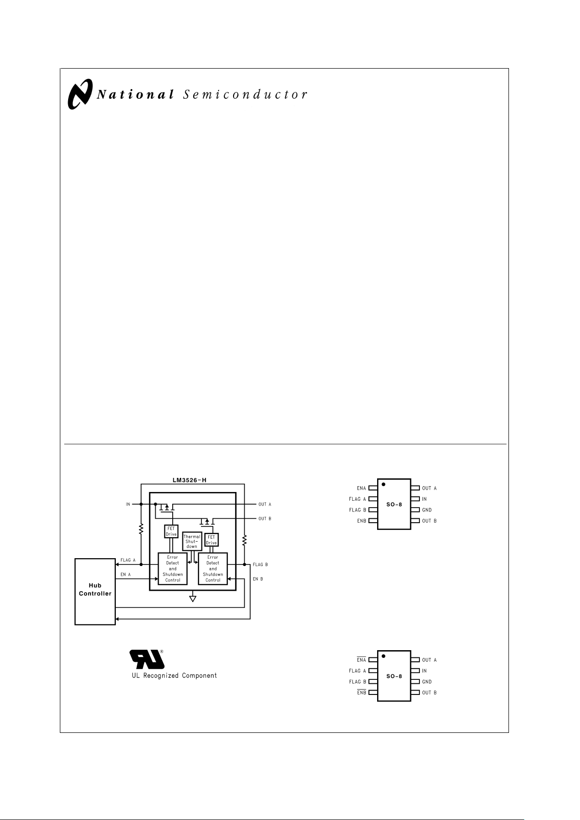
Typical Operating Circuit and Connection Diagram
DS101097-1
DS101097-2
LM3526-H
DS101097-40
DS101097-28
LM3526-L
February 2000
LM3526 Dual Port USB Power Switch and Over-Current Protection
© 2000 National Semiconductor Corporation DS101097 www.national.com
Page 2
Ordering Information
Part Number Enable, Delivery Option Package Type
LM3526M-H Active High Enable, 95 units per rail
SO-8,
NS Package
Number M08A
LM3526M-L Active Low Enable, 95 units per rail
LM3526MX-H Active High Enable, 2500 units per reel
LM3526MX-L Active Low Enable, 2500 units per reel
LM3526
www.national.com 2
Page 3
Absolute Maximum Ratings (Note 1)
If Military/Aerospace specified devices are required,
please contact the National Semiconductor Sales Office/
Distributors for availability and specifications.
Supply Voltage −0.3V to 6V
Output Voltage −0.3V to 6V
Voltage at All Other Pins −0.3V to 5.5V
Power Dissipation (T
A
= 25˚C)
(Note 2) 700 mW
T
JMAX
(Note 2) 160˚C
Operating Ratings
Supply Voltage Range 2.7V to 5.5V
Operating Ambient Range −40˚C to 85˚C
Operating Junction Temperature
Range −40˚C to 125˚C
Storage Temperature Range −65˚C to +150˚C
Lead Temperature
(Soldering, 5 seconds) 260˚C
ESD Rating (Note 3)
ESD Rating Output Only
2kV
8kV
DC Electrical Characteristics
Limits in standard typeface are for T
J
=
25˚C, and limits in boldface type apply over the full operating temperature range. Un-
less otherwise specified: V
IN
=
5.0V, V
EN
=
0V (LM3526-L) or V
EN
=
V
IN
(LM3526-H).
Symbol Parameter Conditions Min Typ Max Units
R
ON
On Resistance
V
IN
=
5V, I
OUT
=
500mA, each switch 100 140
mΩ
V
IN
=
2.7V, I
OUT
=
500mA, each switch 110 180
I
OUT
OUT pins continuous
output current
Each Output 0.5 A
I
SC
Short Circuit Output
Current
Each Output (enable into Load) (Note 4)
V
OUT
=
4.0V
V
OUT
=
0.1V
0.5 1.2
1
1.9
1.5
A
OC
THRESH
Over-current Threshold 2.2 3.2 A
I
LEAK
OUT pins Output
Leakage Current
VEN=VIN(LM3526-L)
VEN= 0V (LM3526-H)
0.01 10 µA
R
FO
FLAG Output Voltage
I
FO
= 10 mA, V
IN
=
5.0V 10 25
ΩI
FO
= 10 mA, V
IN
=
3.3V 11 35
I
FO
= 10 mA, V
IN
=
2.7V 12 40
I
EN
EN/EN Leakage Current VEN/VEN=0VorVEN/VEN=V
IN
−0.5 0.5 µA
V
IH
EN/EN Input Logic High (Note 5) 2.4 1.9 V
V
IL
EN/EN Input Logic Low (Note 5) 1.7 0.8 V
V
UVLO
Under-Voltage Lockout
Threshold
1.8 V
I
DDOFF
Supply Current Switch-Off
−40˚C ≤ T
J
≤ 85˚C
0.2 1
2
µA
I
DDON
Supply Current Switch-On 115 200 µA
Th
SD
Over-temperature
Shutdown Threshold
TJIncreasing, with no shorted output
T
J
Increasing, with shorted output (s)
T
J
Decreasing (Note 4)
150
145
135
˚C
I
FH
Error Flag Leakage
Current
V
flag
=
5V 0.01 1 µA
Note 1: Absolute Maximum Ratings indicate limits beyond which damage to the device may occur. Electrical specifications do not apply when operating the device
beyond its rated operating conditions.
Note 2: The maximum power dissipation must be derated at elevated temperatures and is dictated by T
JMAX
(Maximum junction temperature), θJA(junction to am-
bient thermal resistance), andT
A
(ambient temperature). The maximumallowablepower dissipation at any temperature is P
DMAX
=
(T
JMAX−TA
)/θJAor the number
given in the Absolute Maximum Ratings, which ever is lower. θ
JA
=
150˚C/W.
Note 3: The human body model is a 100 pF capacitor discharged through a 1.5 kΩ resistor into each pin. Enable pin ESD threshold is 1.7kV.
Note 4: Thermal Shutdown will protect the device from permanent damage.
Note 5: For LM3526-L, OFF is EN ≥ 2.4V and ON is EN ≤ 0.8V. For LM3526-H, OFF is EN ≤ 0.8V and ON is EN ≥ 2.4V.
LM3526
www.national.com3
Page 4
AC Electrical Characteristics
Limits in standard typeface are for T
J
=
25˚C, and limits in boldface type apply over the full operating temperature range. Un-
less otherwise specified: V
IN
=
5.0V.
Symbol Parameter Conditions Min Typ Max Units
t
r
OUT Rise Time RL=10Ω 100 µs
t
f
OUT Fall Time RL=10Ω 5µs
t
ON
Turn on Delay, EN to OUT RL=10Ω 150 µs
t
OFF
Turn off Delay, EN to OUT RL=10Ω 5µs
t
OC
Over Current Flag Delay RL=0 1 ms
Pin Description
Pin Number Pin Name Pin Function
1, 4 ENA, ENB
(LM3526-L)
ENA, ENB
(LM3526-H)
Enable (Input): Logic-compatible enable inputs.
2, 3 FLAG A
FLAG B
Fault Flag (Output): Active-low, open-drain outputs. Indicates overcurrent, UVLO or thermal
shutdown.
*
See application section for more information.
6 GND Ground
7 IN Supply Input: This pin is the input to the power switch and the supply voltage for the IC.
8, 5 OUT A
OUT B
Switch Output: These pins are the outputs of the high side switch.
Typical Application Circuit
DS101097-3
LM3526
www.national.com 4
Page 5

Typical Performance Characteristics V
IN
=
5.0V, I
L
=
500 mA, T
A
=
25˚C unless otherwise specified.
R
ON
vs Temperature
DS101097-4
RONvs Temperature
DS101097-5
Quiescent Current vs Input Voltage
DS101097-6
Quiescent Current vs Temperature
DS101097-7
Current Limit vs Output Voltage
DS101097-8
OC Threshold vs Temperature
DS101097-9
LM3526
www.national.com5
Page 6

Typical Performance Characteristics V
IN
=
5.0V, I
L
=
500 mA, T
A
=
25˚C unless otherwise
specified. (Continued)
Fault Flag Delay vs Temperature
DS101097-35
Fault Flag Delay vs Temperature
DS101097-36
Under Voltage Lockout (UVLO)
DS101097-34
Under Voltage Lockout Threshold vs Temperature
DS101097-37
Over Current/Current Limit Response
*
DS101097-10
*
Output is shorted to Ground through a 100 mΩ resistor
Short Circuit Response with
Thermal Cycling
*
DS101097-11
LM3526
www.national.com 6
Page 7

Typical Performance Characteristics V
IN
=
5.0V, I
L
=
500 mA, T
A
=
25˚C unless otherwise
specified. (Continued)
Turn-ON/OFF Response with
47Ω/10µF Load
DS101097-12
Turn-ON/OFF Response with
47Ω/150µF Load
DS101097-13
Thermal Shutdown Response
(Port A output shorted
*
)
DS101097-14
*
Port A is shorted to GND through a 100 mΩ resistor
Thermal Shutdown Response (See Notes)
DS101097-29
Enable into a short
DS101097-30
LM3526
www.national.com7
Page 8

Functional Description
The LM3526-H and LM3526-L are high side P-Channel
switches with active-high and active-low enable inputs, respectively. Fault conditions turn-off and inhibit turn-on of the
output transistor and activate the open-drain error flag transistor sinking current to the ground.
INPUT AND OUTPUT
IN (Input) is the power supply connection to the control circuitry and the source of the output MOSFET.
OUT (Output) is the connection to the drain of the output
MOSFET. In a typical application circuit, current flows
through the switch from IN to OUT towards the load.
If V
OUT
is greater than VINwhen the switch is enabled, current will flow from OUT to IN since the MOSFET is bidirectional.
THERMAL SHUTDOWN
The LM3526 is internally protected against excessive power
dissipation by a two-stage thermal protection circuit. If the
device temperature rises to approximately 145˚C, the thermal shutdown circuitry turns off any switch that is current limited. Non-overloaded switches continue to function normally.
If the die temperature rises above 150˚C, both switches are
turned off and both fault flag outputs are activated. Hysteresis ensures that a switch turned off by thermal shutdown
will not be turned on again until the die temperature is reduced to 135˚C. Shorted switches will continue to cycle off
and on, due to the rising and falling die temperature, until the
short is removed.
UNDERVOLTAGE LOCKOUT
UVLO prevents the MOSFET switch from turning on until input voltage exceeds 1.8V (typical).
If input voltage drops below 1.8V (typical), UVLO shuts off
the MOSFET switch and signals the fault flag. UVLO functions only when device is enabled.
CURRENT LIMIT
The current limit circuit is designed to protect the system
supply, the MOSFET switches and the load from damage
caused by excessive currents. The current limit threshold is
set internally to allow a minimum of 500 mA through the
MOSFET but limits the output current to approximately 1.0A
typical.
FAULT FLAG
The fault flag is an open-drain output capable of sinking
10 mA load current to typically 100 mV above ground.
A parasitic diode exists between the flag pins and V
IN
pin.
Pulling the flag pins to voltages higher than V
IN
will forward
bias this diode and will cause an increase in supply current.
This diode will also clamp the voltage on the flag pins to a diode drop above V
IN
.
The fault flag is active (pulled low) when any of the following
conditions are present: under-voltage, current limit, or thermal shutdown.
A1ms (typ.) delay in reporting the fault condition prevents erroneous fault flags and eliminates the need for an external
RC delay network.
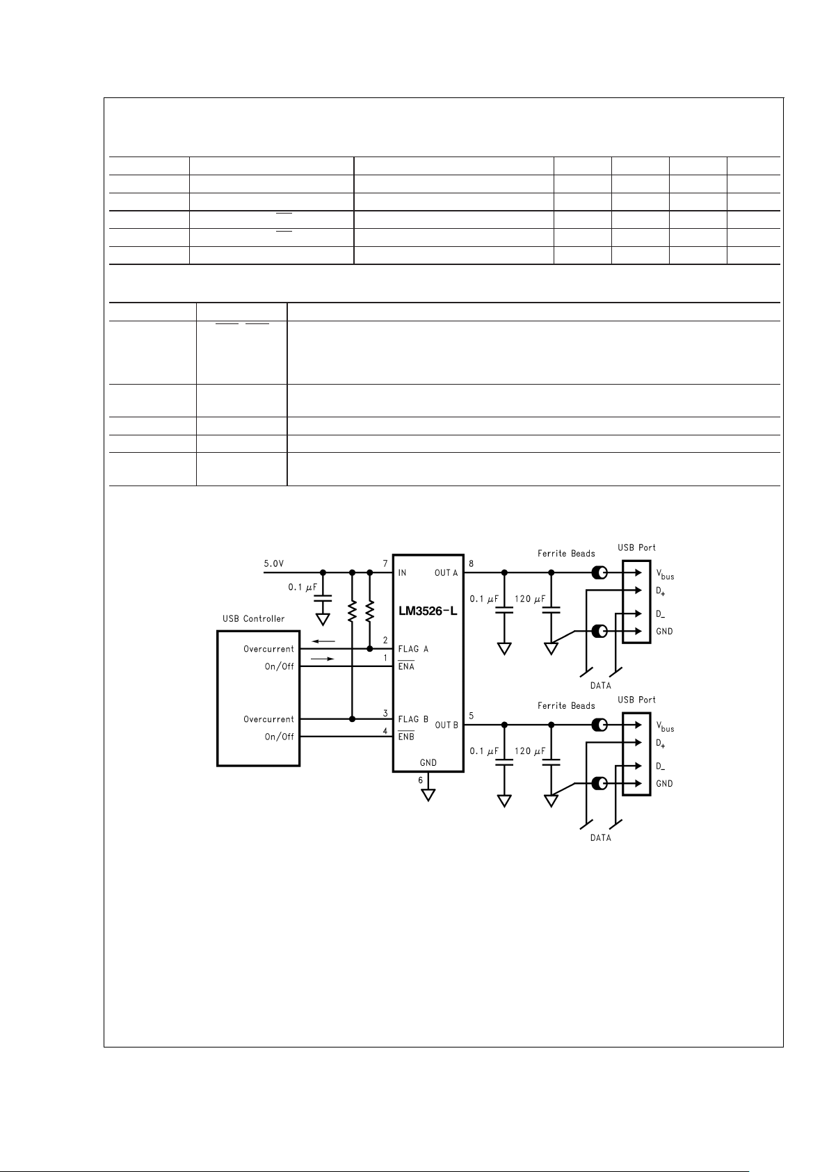
Application Information
FILTERING
The USB specification indicates that “no less than 120 µF
tantalum capacitors” must be used on the output of each
downstream port. This bulk capacitance provides the
short-term transient current needed during a hot plug-in.
Current surges caused by the input capacitance of the down
stream device could generate undesirable EMI signals. Ferrite beads in series with all power and ground lines are recommended to eliminate or significantly reduce EMI.
In selecting a ferrite bead, the DC resistance of the wire used
must be kept to a minimum to reduce the voltage drop.
A 0.01 µF ceramic capacitor is recommended on each port
directly between the V
bus
and ground pins to prevent EMI
damage to other components during the hot-detachment.
Adequate capacitance must be connected to the input of the
device to limit the input voltage drop during a hot-plug event
to less than 330 mV. For a few tens of µs, the host must supply the in-rush current to the peripheral, charging its bulk capacitance to V
bus
. This current is initially supplied by the input capacitor. A 33 µF 16V tantalum capacitor is
recommended.
In choosing the capacitors, special attention must be paid to
the Effective Series Resistance, ESR, of the capacitors to
minimize the IR drop across the capacitor’s ESR.
SOFT START
To eliminate the upstream voltage droop caused by the high
in-rush current drawn by the output capacitors, the maximum
in-rush current is internally limited to 1.5A.
TRANSIENT OVER-CURRENT DELAY
High transient current is also generated when the switch is
enabled and large values of capacitance at the output have
to be rapidly charged. The in-rush currents created could exceed the short circuit current limit threshold of the device
forcing it into the current limit mode. The capacitor is
charged with the maximum available short circuit current set
by the LM3526. The duration of the in-rush current depends
on the size of the output capacitance and load current. Since
this is not a valid fault condition, the LM3526 delays the generation of the fault flag for 1 ms. If the condition persists due
to other causes such as a short, a fault flag is generated aftera1msdelay has elapsed.
The LM3526’s 1 ms delay in issuing the fault flag is adequate
for most applications. If longer delays are required, an RC filter as shown in
Figure 1
may be used.
DS101097-24
FIGURE 1.
LM3526
www.national.com 8
Page 9

Application Information (Continued)
PCB LAYOUT CONSIDERATIONS
In order to meet the USB requirements for voltage drop,
droop and EMI, each component used in this circuit must be
evaluated for its contribution to the circuit performance. The
PCB layout rules and guidelines must be followed.
•
Place the switch as close to the USB connector as possible. Keep all V
bus
traces as short as possible and use at
least 50-mil, 1 ounce copper for all V
bus
traces. Solder
plating the traces will reduce the trace resistance.
•
Avoid vias as much as possible. If vias are used, use multiple vias in parallel and/or make them as large as possible.
•
Place the output capacitor and ferrite beads as close to
the USB connector as possible.
•
If ferrite beads are used, use wires with minimum resistance and large solder pads to minimize connection resistance.
DS101097-23
FIGURE 2. Self-Powered Hub Per-Port Voltage Drop
LM3526
www.national.com9
Page 10

Typical Applications
DS101097-25
FIGURE 3. Dual-Port USB Self-Powered Hub
DS101097-26
FIGURE 4. Soft-Start Application (Single port shown)
DS101097-27
FIGURE 5. In-rush Current-limit Application
LM3526
www.national.com 10
Page 11

Physical Dimensions inches (millimeters) unless otherwise noted
LIFE SUPPORT POLICY
NATIONAL’S PRODUCTS ARE NOT AUTHORIZED FOR USE AS CRITICAL COMPONENTS IN LIFE SUPPORT
DEVICES OR SYSTEMS WITHOUT THE EXPRESS WRITTEN APPROVAL OF THE PRESIDENT AND GENERAL
COUNSEL OF NATIONAL SEMICONDUCTOR CORPORATION. As used herein:
1. Life support devices or systems are devices or
systems which, (a) are intended for surgical implant
into the body, or (b) support or sustain life, and
whose failure to perform when properly used in
accordance with instructions for use provided in the
labeling, can be reasonably expected to result in a
significant injury to the user.
2. A critical component is any component of a life
support device or system whose failure to perform
can be reasonably expected to cause the failure of
the life support device or system, or to affect its
safety or effectiveness.
National Semiconductor
Corporation
Americas
Tel: 1-800-272-9959
Fax: 1-800-737-7018
Email: support@nsc.com
National Semiconductor
Europe
Fax: +49 (0) 180-530 85 86
Email: europe.support@nsc.com
Deutsch Tel: +49 (0) 69 9508 6208
English Tel: +44 (0) 870 24 0 2171
Français Tel: +33 (0) 1 41 91 8790
National Semiconductor
Asia Pacific Customer
Response Group
Tel: 65-2544466
Fax: 65-2504466
Email: ap.support@nsc.com
National Semiconductor
Japan Ltd.
Tel: 81-3-5639-7560
Fax: 81-3-5639-7507
www.national.com
See Order Information Table
NS Package Number M08A
LM3526 Dual Port USB Power Switch and Over-Current Protection
National does not assume any responsibility for use of any circuitry described, no circuit patent licenses are implied and National reserves the right at any time without notice to change said circuitry and specifications.
 Loading...