

Page 1
LM15 0/2 50
LM350
March1993
ADJUSTABLE VOLTAGE REGULATORS
THREE-TERMINAL 3 A
.GUARANTEED 3A OUTPUTCURRENT
.ADJUSTABLE OUTPUT DOWN TO 1.2V
.LINE REGULATIONTYPICALLY 0.005% /V
.LOAD REGULATION TYPICALLY0.1%
.GUARANTEED THERMAL REGULATION
.CURRENT LIMIT CONSTANT WITH TEM-
PERATURE
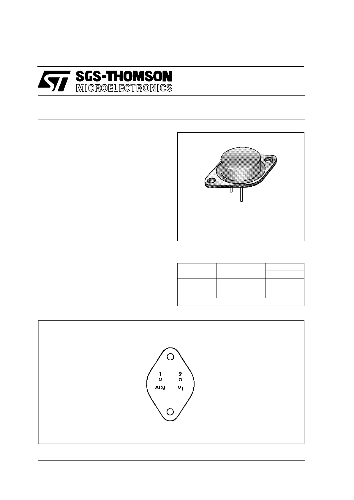
.STANDARD3-LEAD TRANSISTOR PACKAGE
TO3
K SUFFIX
(SteelCan)
ORDER CODE
PART
NUMBER
TEMPERATURE
RANGE
PACKAGE
K
LM150
LM250
LM350
-55
o
C to + 150oC
-25
o
C to + 150oC
0oC to + 125oC
•
•
•
EXAMPLE: LM150K
PIN CONNE CTI O N
(bottom view)
Case is output
1/7
Page 2
ABSOLUTE MAXIMUM RATING
Symbol Parameter Value Unit
P
tot
Power Dissipation Internally Limited W
V
I-VO
Input-Output Voltage DIfferential 35 V
T
oper
Operating Junction Temperature Range LM150
LM250
LM350
-55 to 150
-25 to 150
0 to 125
o
C
T
stg
Storage Temperature Range -65 to 150
o
C
T
lead
Lead Temperature (Soldering, 10 seconds) 300
o
C
THERMAL CHARACTERISTICS
Symbol Parameter Value Unit
R
th(j-c)
Typical Junction-Case Thermal Resistance 1.5
o
C/W
R
th(j-a)
Max Junction-Ambient Thermal Resistance 35
o
C/W
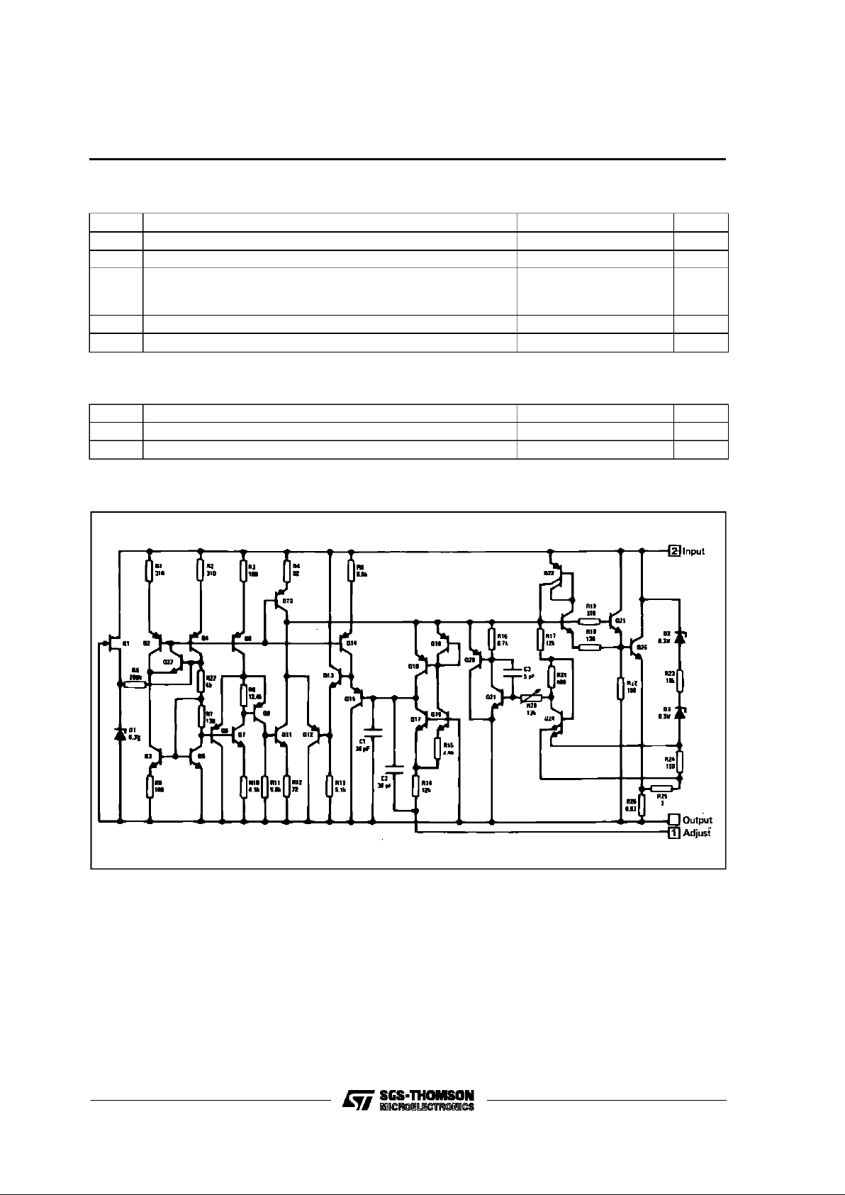
SCHEM ATIC DIA GRA M
LM150-LM250-LM350
2/7
Page 3
ELECTRICAL CHARACTERISTICS
LM150: -55oC ≤ Tj≤ 150oC, VI-VO= 5V, IO= 1.5A
LM250: -25oC ≤ Tj≤ 150oC, VI-VO= 5V, IO= 1.5A
LM350: 0oC ≤ Tj≤ 150oC, VI-VO= 5V, IO= 1.5A
Although power dissipation is internally limited, these specifications apply to power dissipation up to
30W (unless otherwise specified).
Symbol Parameter LM150-LM250 LM350 Unit
Min. Typ. Max. Min. Typ. Max.
K
VI
Line Regulation - (note 1)
T
amb
=25oC, 3 V ≤ (VI-VO)≤35 V
0.005 0.01 0.005 0.03 %/V
K
VO
Load Regulation T
amb
=25oC, 10 mA ≤ IO≤ 3A
VO≤5V - (note 1)
VO≥ 5V - (note 1)
5
0.1150.3
5
0.1250.5
mV
%
Thermal Regulation (pulse = 20 ms) 0.002 0.01 0.002 0.02 %/W
I
adj
Adjustment Pin Current 50 100 50 100 µA
∆I
adj
Adjustment Pin Current Change
10 mA ≤ IL≤ 3A,3V≤(VI-VO)≤35 V
0.2 5 0.2 5 µA
v
(ref)
Reference Voltage
3V ≤ (VI-VO)≤35 V, 10 mA ≤ IO≤ 3A, P ≤ 30W
1.19 1.24 1.29 1.19 1.24 1.29 V
K
VI
Line Regulation - (note 1)
3V≤(VI-VO)≤35 V
0.02 0.05 0.02 0.05 %/V
K
VO
Load Regulation 10 mA ≤ IO≤ 3A
VO≤5V - (note 1)
VO≥ 5V - (note 1)
20
0.3
50
1
20
0.3701.5
mV
%
K
VT
Temperature Stability (T
min
≤ Tj≤ T
max
)11%
I
O(min)
Minimum Load Current (VI-VO≤35 V) 3.5 5 3.5 10 mA
I
O(max)
Current Limit (VI-VO≤10 V)
DC
V
I-VO
=30V
3 4.5
1
3 4.5
1
A
RMS Output Noise, % of V
O
(T
amb
=25oC, 10 Hz ≤ f ≤ 10 KHz)
0.001 0.001 %
R
vf
Ripple Rejection Ratio
VO= 10 V, f = 120 Hz
C
adi
=10µF66
65
86 66
65
86
dB
K
VH
Long Term Stability (T
amb
= 125oC) 0.3 1 0.3 1 %
Note 1 : Regulation is measured at constant junction temperature. Changes in output voltage due to heating effects are taken
into account separately by thermal rejection.
LM150-LM250-LM350
3/7
Page 4

TYPICAL AP PLI CA TI O NS
+ 1.2V to + 25V ADJUSTABLE REGULATOR
APPLICATION HINTS
In operation,the LM350 develops anominal 1.25V
reference voltage, V
(ref)
, between the output and
adjustment terminal. The reference voltage is impressed across program resistor R1and, since the
voltage is constant, aconstant current I1then flows
through theoutput set resistor R2, giving an output
voltage of
VO=V
(ref)
(1+
R
2
R
1
)+I
adjR2
Figure 1.
Since the 50µAcurrent from the adjustment terminal represents an error term, theLM350 was designed to minimize I
adj
and make it very constant
withlineand load changes. To do this, allquiescent
operating current is returned to the output establishing a minimum load currentrequirement. Ifthere
is insufficientloadonthe output, the outputwill rise.
EXTERNAL CAPACITORS
An input bypass capacitor is recommended. A
0.1µFdisc or1µFsolid tantalum on the inputis suitable input by passing for almost all applications.
Thedeviceismore sensitivetothe absenceofinput
bypassing when adjustment or output capacitors
are used byt the above values will eliminate the
possibility of problems.
The adjustment terminal can be bypassed to
ground on the LM350 to improve ripple rejection.
This bypass capacitor prevents ripple form being
amplified as the output voltage is increased. With
a10µF bypass capacitor 75dB ripple rejection is
obtainableatanyoutputlevel.Increases over20µF
do not appreciably improve the ripple rejection at
frequencies above 120Hz. If the bypass capacitor
is used, it is sometimes necessary to include protection diodes to prevent the capacitor from discharging through internal low current paths and
damaging the device.
In general, the best type of capacitors to use are
solid tantalum. Solid tantalumcapacitors have low
impedance even at high frequencies. Depending
upon capacitorconstruction, it takes about 25µFin
aluminumelectrolyticto equal1µFsolid tantalum at
high frequencies. Ceramic capacitors are also
good at high frequencies, but some types have a
large decrease in capacitance at frequencies
around 0.5MHz. For this reason,0.01µF disc may
seem towork better than a0.1µF discas a bypass.
Although the LM350 is stable with no output capacitors, like any feedback circuit, certain values of
external capacitancecan cause excessive ringing.
This occurs with values between 500pF and
5000pF. A 1µF solid tantalum(or 25µF aluminium
electrolytic) on the output swamps this effect and
insures stability.
LOADREGULATION
The LM350is capable ofproviding extremely good
load regulation but a few precautions are needed
to obtain maximum performance. The current set
resistor connected between the adjustment terminal and the output terminal (usually 240Ω) should
be tied directly tothe output of the regulator rather
than near the load. This eliminates line drops from
appearing effectively in series with the reference
and degrading regulation. For example, a 15V
regulator with 0.05Ωresistance between theregulator and loadwill have a load regulationdue to line
resistance of 0.05Ω xIL. If the set resistor is connected near the load the effective line resistance
∆ Needed if device is far from filter capacitors.
*
Optional-improves transient response. Output capacitors in the
range of 1µF to 100µF of aluminium or tantalum electrolytic are
commonlyused toprovide improvedoutput impedance and rejection of transients.
R2
** VO=1.25V(1+ )
R1
*** R1=240Ωfor LM150 and LM250
LM 350
LM 350
LM150-LM250-LM350
4/7
Page 5

will be 0.05Ω(1 + R2/R1)or in this case, 11.5times
worse.
Figure 2showsthe effect of resistance between the
regulator and 140Ω set resistor.
Withthe TO-3package,itis easytominimizetheresistance from the case to the set resistor, by using
2 separate leadsto the case. The ground of R2 can
be returned near the ground of the load to provide
remote ground sensing and improve load regulation.
PROTECTION DIODES
WhenexternalcapacitorsareusedwithanyICregu-
lator it is sometimes necessary to add protection
diodes to prevent the capacitors from discharging
through low current points into the regulator. Most
Figure 2 : Regulator with LineResistance in Out-
put Lead.
20µF capacitors have lowenoughinternal seriesresistance to deliver 20A spikes when shorted. Althoughthe surgeis short,there is enough energy to
damage parts of the IC.
When an output capacitor is connected to a regulator and theinput is shorted, the outputcapacitorwill
discharge into the outputof the regulator. The dischargecurrentdepends on the value of thecapacitor, theoutputvoltage ofthe regulator, and therate
of decrease of VI. Inthe LM350 this discharge path
is through alarge junctionthatisable to sustain25A
surgewithno problem.Thisis nottrue ofother types
of positive regulators. For output capacitors of
100µF or less at output of 15V or less, there is no
need to use diodes.
The bypass capacitor on the adjustment terminal
can discharge through a low current junction. Discharge occurs when either the input or output is
shorted. Internal to the LM350 is a 50Ω resistor
which limits the peakdischargecurrent. No protectionis neededforoutputvoltages of 25V or less and
10µF capacitance. Figure 3 shows an LM350 with
protection diodes included for use with outputs
greaterthan 25Vand high valuesof output capacitance.
Figure 3 : Regulator with Protection Diodes.
LM350
LM350
LM150-LM250-LM350
5/7
Page 6

DIM.
mm inch
MIN. TYP. MAX. MIN. TYP. MAX.
A 11.00 13.10 0.433 0.516
B 0.97 1.15 0.038 0.045
C 1.50 1.65 0.059 0.065
D 8.32 8.92 0.327 0.351
E 19.00 20.00 0.748 0.787
G 10.70 11.10 0.421 0.437
N 16.50 17.20 0.649 0.677
P 25.00 26.00 0.984 1.023
R 4.00 4.09 0.157 0.161
U 38.50 39.30 1.515 1.547
V 30.00 30.30 1.187 1.193
C
D
N
B
V
U
R
A
P
E
G
O
P003F
TO-3 MECHANICAL DATA
LM150-LM250-LM350
6/7
Page 7

Information furnished is believed to be accurate and reliable.However, SGS-THOMSON Microelectronics assumes no responsability for the
consequences of useof such information nor for any infringementof patents or other rights of third parties which may results from its use. No
license isgranted by implication or otherwise underany patent or patent rights ofSGS-THOMSON Microelectronics. Specificationsmentioned
in this publication are subject to changewithout notice.This publication supersedes andreplaces all information previously supplied.
SGS-THOMSON Microelectronicsproductsare not authorized foruse ascritical componentsinlife supportdevices orsystems without express
written approval of SGS-THOMSON Microelectonics.
1994 SGS-THOMSON Microelectronics- All RightsReserved
SGS-THOMSON Microelectronics GROUP OF COMPANIES
Australia - Brazil - France- Germany - Hong Kong - Italy - Japan - Korea - Malaysia - Malta - Morocco - The Netherlands-
Singapore - Spain - Sweden- Switzerland -Taiwan - Thailand - UnitedKingdom -U.S.A
LM150-LM250-LM350
7/7
 Loading...