

Page 1
www.fairchildsemi.com
LM350
3-Terminal 3A Positive Adjustable Voltage
Regulator
Features
• Output adjustable betwe en 1.2V an d 33V
• Guaranteed 3A output current
• Internal thermal overload protection
• Load regulation (Typ: 0.1%)
• Line regulation (Typ: 0.015%/V)
• Internal short-circuit current limit
• Output transistor safe-area compensation
Description
The LM350 is an adjustable 3-terminal positive voltage
regulator capable of supplying in excess of 3.0 A over an
output voltage range of 1.2V to 33 V
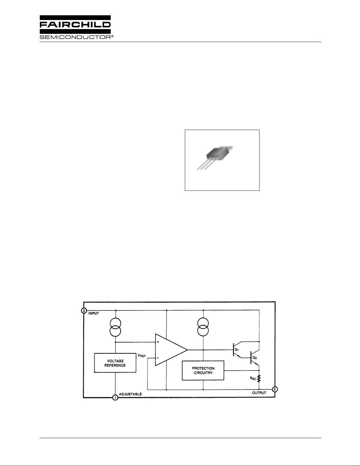
TO-220
1
1. Adj 2. O utput 3. Input
Internal Block Diagram
©2001 Fairchild Semiconductor Corporation
Rev. 1.0.0
Page 2
LM350
Absolute Maximum Ratings
Parameter Symbol Value Unit
Input-Output Voltage Differential V
Lead Temperature (Soldering, 10sec) T
I
LEAD
Power Dissipation P
Operating Temperature Range T
Storage Temperature Range T
- V
D
OPR
STG
O
35 V
300 °C
Internally limited -
0 ~ +125 °C
-65 ~ +150 °C
Electrical Characteristics
(VI-VO=5V, IO=1.5A, TJ=0°C to + 125°C; P
D ≤ PDMAX
, unless otherwise specified)
DC
Parameter Symbol
Line Regulation (Note1) Rline T
Load Regulation (Note1)
Adjustment Pin Current I
Adjustment Pin Current
Change
Rload
ADJ
∆I
ADJ
Thermal Regulation REG
Reference Voltage V
REF
= +25°C, 3V ≤ VI -V
A
T
= +25
A
V
≤ 5V
O
V
≥ 5V
O
3V ≤ VI -V
10mA ≤ I
Pulse = 20ms, TA =+ 25°C - 0.002 - %/W
T
3V ≤ VI -V
Line Regulation Rline 3.0V ≤ V
Load Regulation
Rload
Temperature Stability ST
Maximum Output Current
Minimum Load Current I
RMS Noise, %of V
OUT
Ripple Rejection
Long-Term Stability
I
o(MAX)
L(MIN)VI
V
RR
ST
10mA ≤ I
V
≤ 5.0V
O
V
≥ 5.0V
O
TJ = 0°C to + 125°C-1.0-%
T
VI -V
O
-VO = 30V, P
V
I
-VO = 35V - 3.5 10 mA
10Hz ≤ f ≤ 10KHz, TA= +25
N
V
= 10V, f = 120Hz,
O
C
= 0
ADJ
C
= 10µF66
ADJ
T
=+125
J
Conditions
°C, 3V ≤ V
≤ 35V - 0.015 0.03 %/V
O
≤ 35V
I -VO
Min. Typ. Max. Unit
-5
0.1250.5
- - 50 100 µA
≤ 35V,
O
≤ 3A, PD ≤ P
o
≤ 35V, 10mA ≤I O≤ 3A,P
O
≤ 35V - 0.02 0.07 %/W
I -VO
≤ 3.0A
O
MAX
≤ 30W 1.2 1.25 1.30 V
D
0.2 5.0 µA
-
-20
0.3701.5
≤ 10V, PD ≤ P
≤ P
D
MAX
MAX,TA
= +25°C 0.25 1.0 - A
°C - 0.003 - %/V
3.0 4.5 - A
65
80
°C
0.3 1 %/
-
mV
%
mV
%
o
dB
dB
1000HR
Note:
1. Regulation is measured at con stant junctio n temp eratur e. Cha nges in output v oltage due to he ating e ffect s must be taken in to
account separately. Pulse testing with low duty cycle is used.
2
Page 3
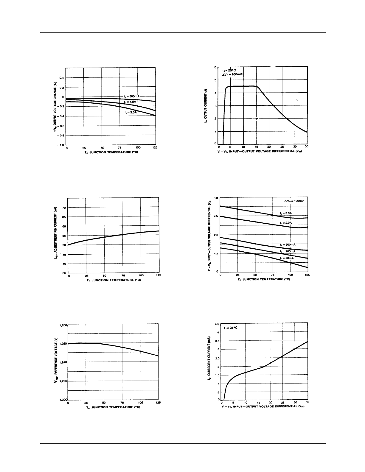
Typical Perfomance Characteristics
LM350
Figure 1. Load Regulation
Figure 3. Adjustment Pin Current
Figure 2. Current Limit
Figure 4. Dropout Voltage
Figure 5. Temperature Stability
Figure 6. Minimum Load Current
3
Page 4

LM350
Typical Perfomance Characteristics (continued)
Figure 7. Ripple Rejection vs Vo
Figure 9. Ripple Re jection vs Frequency
Figure 8. Ripple Rejection vs Io
Figure 10. Output Impedance
Figure 11. Line Transient Response
Figure 12. Load Transient Response
4
Page 5

Typical Application
LM350
Input
C
: CI is required if the regulator is located an appreciable distance from power supply filter.
I
C
: Output capacitors in the range of 1µF to 100µF of aluminum or tantalum electronic are commonly used to provide
O
LM350
Figure 13.
Output
improved out put impedan ce and rejection of transients.
In operation, th e LM 350 deve lops a nom ina l 1. 25V refe ren ce vol tag e, V
reference voltage is impressed across program resistor R
through the output set resistor R
= 1.25V(1+R2/R1) + I
V
O
Since I
mize I
current (less than 100µF) from the adjustment terminal represents an error term, the LM350 was designed to mini-
ADJ
and make it very constant with line and load changes. To do this, all quiescent operating current is returned to the
ADJ
, giving an output voltage of
2
ADJ R2
and, since the voltage is constant, a constant current I1 then flows
1
, between the output and adjustment terminal. The
REF
output establishing a minimum load current requirement. If there is insufficient load on the output, the output voltage will rise.
Since the LM350 is a floating regulator, it is only the voltage differential across the circuit which is important to performance,
and operation at high voltage with respect to ground is possible.
Since I
is controlled to less than 100µA, the error associated with this term is negligible in most applications.
ADJ
5
Page 6

LM350
Mechanical Dimensions
Package
9.90
±0.20
(8.70)
(1.70)
±0.20
9.20
±0.10
1.30
(1.46)
ø3.60
±0.10
(Continued)
(3.70)(3.00)
(45°)
TO-220
±0.10
2.80
±0.20
18.95MAX.
15.90
4.50
1.30
±0.20
+0.10
–0.05
±0.20
13.08
(1.00)
1.27
2.54TYP
±0.20
[2.54
±0.10
]
10.00
±0.20
1.52
±0.10
0.80
±0.10
2.54TYP
±0.20
[2.54
±0.30
10.08
+0.10
0.50
–0.05
2.40
±0.20
]
6
Page 7

Ordering Information
Product Number Package Operating Temperature
LM350T TO-220 0°C to + 125°C
LM350
7
Page 8

LM350
DISCLAIMER
FAIRCHILD SEMICONDUCTOR RESERVES THE RIGHT TO MAKE CHANGES WITHOUT FURT HER NOTICE TO ANY
PRODUCTS HEREI N TO IMPROVE RELIABILITY, FUNCTIO N OR DESIGN. FAIRCH IL D DOES NOT ASSUME ANY
LIABILITY ARISING OUT OF THE APPLICATION OR USE OF ANY PRODUCT OR CIRCUIT DESCRIBED HEREIN; NEITHER
DOES IT CONVEY ANY LICENSE UNDER IT S PATENT RIGHTS, NOR THE RIGHTS OF OTHE RS.
LIFE SUPPORT POL I CY
FAIRCHILD’S PR ODUCTS ARE NOT AUTH ORIZED FOR USE AS C RITICAL COMPONENT S IN LIFE SUPPORT DE VICES
OR SYSTEMS WITHOUT THE EXPRESS WRITTEN APPROVAL OF THE PRESIDENT OF FAIRCHILD SEMICONDUCTOR
CORPORATION. As used herein :
1. Life support devices or systems are devices or systems
which, (a) are intended for surgical implant into the body,
or (b) support or sustain life, and (c) whose failure to
perform when properly used in accordance with
2. A critical component in any component of a life support
device or sy stem whose fai lure to perform can be
reasonably expec ted to cause the failur e of the life support
device or system, or to affect its safety or effec t iv ene ss .
instructions for use provided in the labeling, can be
reasonably expected to result in a significant injury of the
user.
www.fairchildsemi.com
6/1/01 0.0m 001
2001 Fairchild Semiconductor Corporation
Stock#DSxxxxxxxx
 Loading...