

Page 1
November 1, 2007
LM34919
40V, 600 mA Step Down COT Switching Regulator
General Description
The LM34919 Step Down Switching Regulator features all of
the functions needed to implement a low cost, efficient, buck
bias regulator capable of supplying 0.6A to the load. This buck
regulator contains an N-Channel Buck Switch, and is available in a micro SMD package. The constant on-time feedback
regulation scheme requires no loop compensation, results in
fast load transient response, and simplifies circuit implementation. The operating frequency remains constant with line
and load variations due to the inverse relationship between
the input voltage and the on-time. The valley current limit results in a smooth transition from constant voltage to constant
current mode when current limit is detected, reducing the frequency and output voltage, without the use of foldback. Additional features include: VCC under-voltage lockout, thermal
shutdown, gate drive under-voltage lockout, and maximum
duty cycle limiter.
Features
■
Integrated N-Channel buck switch
■
Integrated start-up regulator
■
Input Voltage Range: 8V to 40V
■
No loop compensation required
■
Ultra-Fast transient response
■
Operating frequency remains constant with load current
and input voltage
■
Maximum switching frequency: 1.6 MHz
■
Maximum Duty Cycle Limited During Start-Up
■
Adjustable output voltage
■
Valley Current Limit At 0.64A
■
Precision internal reference
■
Low bias current
■
Highly efficient operation
■
Thermal shutdown
Typical Applications
■
High Efficiency Point-Of-Load (POL) Regulator
■
Non-Isolated Telecommunication Buck Regulator
■
Secondary High Voltage Post Regulator
Package
■
micro SMD
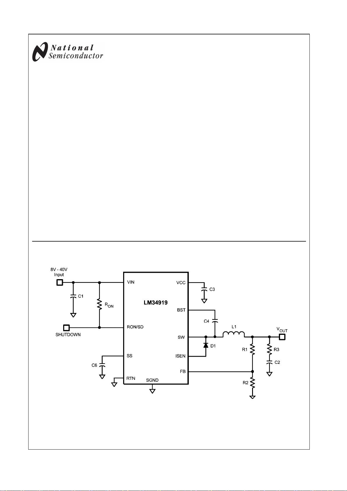
Basic Step Down Regulator
30004431
© 2007 National Semiconductor Corporation 300044 www.national.com
LM34919 40V, 600 mA Step Down COT Switching Regulator
Page 2
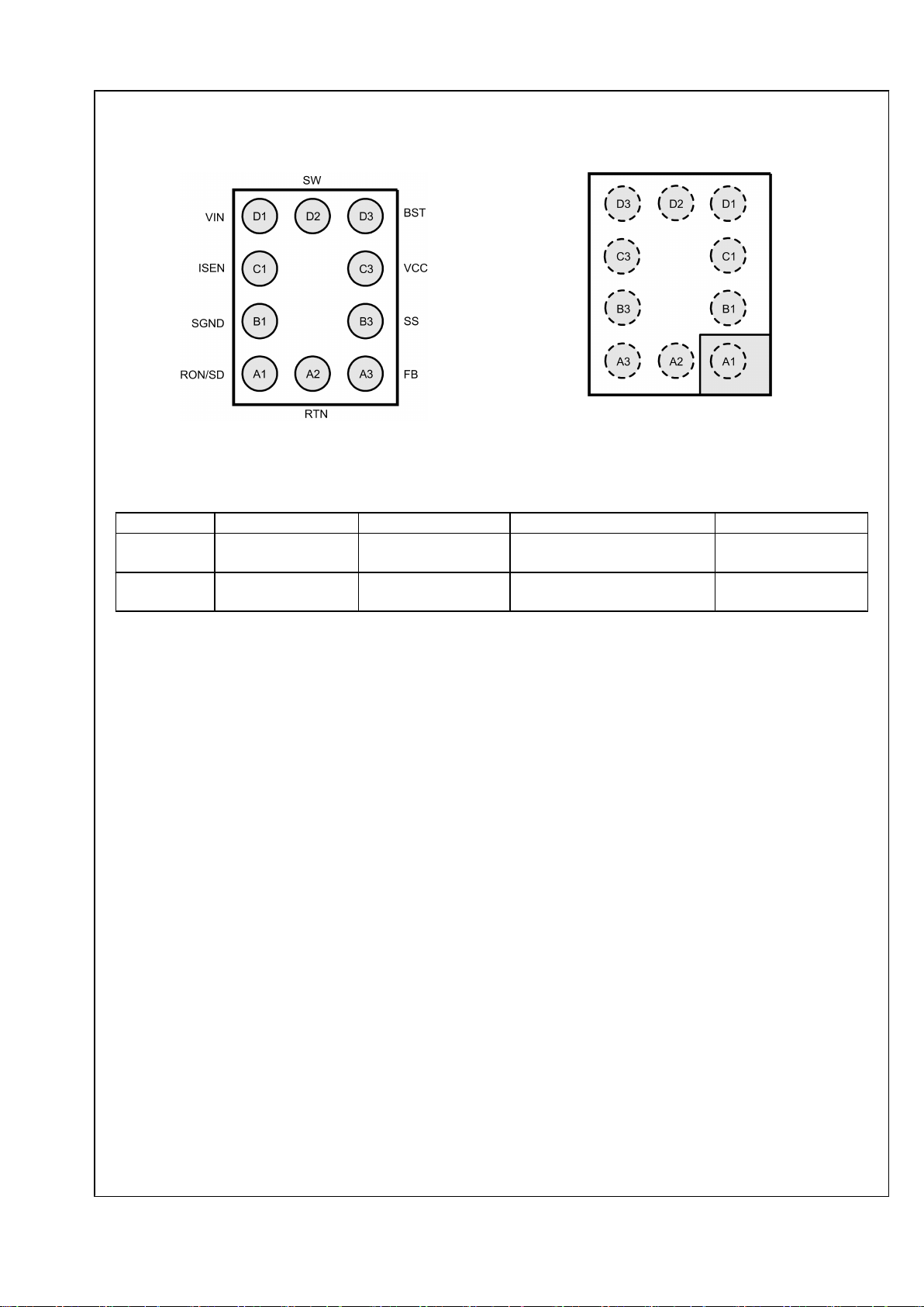
Connection Diagrams
30004402
Bump Side
30004433
Top View
Ordering Information
Order Number Package Type NSC Package Drawing Junction Temperature Range Supplied As
LM34919TL 10-Bump micro SMD TLP10A1A −40°C to + 125°C 250 Units on Tape and
Reel
LM34919TLX 10-Bump micro SMD TLP10A1A −40°C to + 125°C 3000 Units on Tape and
Reel
www.national.com 2
LM34919
Page 3
Pin Descriptions
Pin Number Name Description Application Information
A1 RON/SD On-time control and shutdown An external resistor from VIN to this pin sets the buck switch
on-time. Grounding this pin shuts down the regulator.
A2 RTN Circuit Ground Ground for all internal circuitry other than the current limit
detection.
A3 FB Feedback input from the regulated
output
Internally connected to the regulation and over-voltage
comparators. The regulation level is 2.5V.
B1 SGND Sense Ground Re-circulating current flows into this pin to the current sense
resistor.
B3 SS Softstart An internal current source charges an external capacitor to
2.5V, providing the softstart function.
C1 ISEN Current sense The re-circulating current flows through the internal sense
resistor, and out of this pin to the free-wheeling diode.
Current limit is nominally set at 0.64A.
C3 VCC Output from the startup regulator Nominally regulates at 7.0V. An external voltage (7V-14V)
can be applied to this pin to reduce internal dissipation. An
internal diode connects VCC to VIN.
D1 VIN Input supply voltage Nominal input range is 8.0V to 40V.
D2 SW Switching Node Internally connected to the buck switch source. Connect to
the inductor, free-wheeling diode, and bootstrap capacitor.
D3 BST Boost pin for bootstrap capacitor Connect a 0.022 µF capacitor from SW to this pin. The
capacitor is charged from VCC via an internal diode during
each off-time.
3 www.national.com
LM34919
Page 4
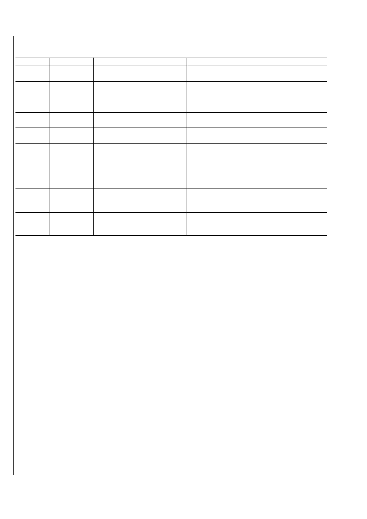
Absolute Maximum Ratings (Note 1)
If Military/Aerospace specified devices are required,
please contact the National Semiconductor Sales Office/
Distributors for availability and specifications.
VIN to RTN 44V
BST to RTN 52V
SW to RTN (Steady State) -1.5V
ESD Rating (Note 2)
Human Body Model 2kV
BST to VCC 44V
VIN to SW 44V
BST to SW 14V
VCC to RTN 14V
SGND to RTN -0.3V to +0.3V
SS to RTN -0.3V to 4V
All Other Inputs to RTN -0.3 to 7V
Storage Temperature Range -65°C to +150°C
JunctionTemperature 150°C
Operating Ratings (Note 1)
VIN 8.0V to 40V
Junction Temperature −40°C to + 125°C
Electrical Characteristics Specifications with standard type are for T
J
= 25°C only; limits in boldface type apply
over the full Operating Junction Temperature (TJ) range. Minimum and Maximum limits are guaranteed through test, design, or
statistical correlation. Typical values represent the most likely parametric norm at TJ = 25°C, and are provided for reference
purposes only. Unless otherwise stated the following conditions apply: VIN = 12V, RON = 200kΩ. See (Note 5).
Symbol Parameter Conditions Min Typ Max Units
Start-Up Regulator, V
CC
VCCReg VCC regulated output 6.6 7 7.4 V
VIN-VCC dropout voltage I
CC
= 0 mA,
VCC = UVLO
VCC
+ 250 mV
1.2 V
VCC output impedance
0 mA ≤ ICC ≤ 5 mA, VIN = 8V
175
Ω
VCC current limit (Note 3) VCC = 0V 9.5 mA
UVLO
VCCVCC
under-voltage lockout threshold VCC increasing 5.7 V
UVLO
VCC
hysteresis VCC decreasing 150 mV
UVLO
VCC
filter delay 100 mV overdrive 3 µs
I
Q
IIN operating current Non-switching, FB = 3V, SW = Open 0.5 0.8 mA
I
SD
IIN shutdown current RON/SD = 0V, SW = Open 75 150 µA
Switch Characteristics
Rds(on) Buck Switch Rds(on) I
TEST
= 200 mA 0.5 1.0
Ω
UVLO
GD
Gate Drive UVLO V
BST
- VSW Increasing 3.0 4.4 5.2 V
UVLOGD hysteresis 480 mV
Softstart Pin
V
SS
Pull-up voltage 2.5 V
Internal current source VSS = 1V 10.5 µA
Current Limit
I
LIM
Threshold Current out of ISEN 0.52 0.64 0.76 A
Resistance from ISEN to SGND 140
mΩ
Response time 150 ns
On Timer
tON - 1 On-time
VIN = 10V, RON = 200 kΩ
2.1 2.77 3.5 µs
tON - 2 On-time
VIN = 40V, RON = 200 kΩ
700 ns
Shutdown threshold Voltage at RON/SD rising 0.45 0.8 1.2 V
Threshold hysteresis Voltage at RON/SD 25 mV
Off Timer
t
OFF
Minimum Off-time 155 ns
Regulation and Over-Voltage Comparators (FB Pin)
V
REF
FB regulation threshold SS pin = steady state 2.440 2.5 2.550 V
FB over-voltage threshold 2.9 V
FB bias current FB = 3V 1 nA
www.national.com 4
LM34919
Page 5
Symbol Parameter Conditions Min Typ Max Units
Thermal Shutdown
T
SD
Thermal shutdown temperature 175 °C
Thermal shutdown hysteresis 20 °C
Thermal Resistance
θ
JA
Junction to Ambient
0 LFPM Air Flow
61 °C/W
Note 1: Absolute Maximum Ratings are limits beyond which damage to the device may occur. Operating Ratings are conditions under which operation of the
device is intended to be functional. For guaranteed specifications and test conditions, see the Electrical Characteristics.
Note 2: The human body model is a 100pF capacitor discharged through a 1.5kΩ resistor into each pin.
Note 3: VCC provides self bias for the internal gate drive and control circuits. Device thermal limitations limit external loading
Note 4: For detailed information on soldering micro SMD package, refer to the Application Note AN-1112.
Note 5: Typical specifications represent the most likely parametric norm at 25°C operation.
5 www.national.com
LM34919
Page 6
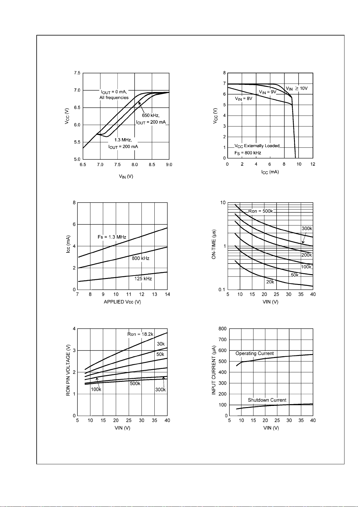
Typical Performance Characteristics
VCC vs V
IN
30004404
VCC vs I
CC
30004405
ICC vs Externally Applied V
CC
30004435
ON-TIME vs VIN and R
ON
30004436
Voltage at the R
ON/SD
Pin
30004437
Shutdown and Operating Current into V
IN
30004438
www.national.com 6
LM34919
Page 7

Typical Application Circuit and Block Diagram
30004401
7 www.national.com
LM34919
Page 8

30004434
FIGURE 1. Start Up Sequence
Functional Description
The LM34919 Step Down Switching Regulator features all the
functions needed to implement a low cost, efficient buck bias
power converter capable of supplying at least 0.6A to the load.
This high voltage regulator contains an N-Channel buck
switch, is easy to implement, and is available in micro SMD
package. The regulator’s operation is based on a constant ontime control scheme, where the on-time is determined by
VIN. This feature allows the operating frequency to remain
relatively constant with load and input voltage variations. The
feedback control requires no loop compensation resulting in
very fast load transient response. The valley current limit detection circuit, internally set at 0.64A, holds the buck switch
off until the high current level subsides. This scheme protects
against excessively high current if the output is short-circuited
when VIN is high.
The LM34919 can be applied in numerous applications to efficiently regulate down higher voltages. Additional features
include: Thermal shutdown, VCC under-voltage lockout, gate
drive under-voltage lockout, and maximum duty cycle limiter.
Control Circuit Overview
The LM34919 buck DC-DC regulator employs a control
scheme based on a comparator and a one-shot on-timer, with
the output voltage feedback (FB) compared to an internal reference (2.5V). If the FB voltage is below the reference the
buck switch is turned on for a time period determined by the
input voltage and a programming resistor (RON). Following the
on-time the switch remains off until the FB voltage falls below
the reference but not less than the minimum off-time. The
buck switch then turns on for another on-time period. Typically, during start-up, or when the load current increases
suddenly, the off-times are at the minimum. Once regulation
is established, the off-times are longer.
When in regulation, the LM34919 operates in continuous conduction mode at heavy load currents and discontinuous conduction mode at light load currents. In continuous conduction
mode current always flows through the inductor, never reaching zero during the off-time. In this mode the operating frequency remains relatively constant with load and line
variations. The minimum load current for continuous conduc-
www.national.com 8
LM34919
Page 9

tion mode is one-half the inductor’s ripple current amplitude.
The operating frequency is approximately:
(1)
The buck switch duty cycle is approximately equal to:
(2)
In discontinuous conduction mode current through the inductor ramps up from zero to a peak during the on-time, then
ramps back to zero before the end of the off-time. The next
on-time period starts when the voltage at FB falls below the
reference - until then the inductor current remains zero, and
the load current is supplied by the output capacitor. In this
mode the operating frequency is lower than in continuous
conduction mode, and varies with load current. Conversion
efficiency is maintained at light loads since the switching losses decrease with the reduction in load and frequency. The
approximate discontinuous operating frequency can be calculated as follows:
(3)
where RL = the load resistance.
The output voltage is set by two external resistors (R1, R2).
The regulated output voltage is calculated as follows:
V
OUT
= 2.5 x (R1 + R2) / R2
Output voltage regulation is based on ripple voltage at the
feedback input,normally obtained from the output voltage ripple through the feedback resistors. The LM34919 requires a
minimum of 25 mV of ripple voltage at the FB pin. In cases
where the capacitor’s ESR is insufficient additional series resistance may be required (R3).
Start-Up Regulator, V
CC
The start-up regulator is integral to the LM34919. The input
pin (VIN) can be connected directly to line voltage up to 40V,
with transient capability to 44V. The VCC output regulates at
7.0V, and is current limited at 9.5 mA. Upon power up, the
regulator sources current into the external capacitor at VCC
(C3). When the voltage on the VCC pin reaches the undervoltage lockout threshold of 5.7V, the buck switch is enabled
and the Softstart pin is released to allow the Softstart capacitor (C6) to charge up.
The minimum input voltage is determined by the regulator’s
dropout voltage, the VCC UVLO falling threshold (≊5.55V),
and the frequency. When VCC falls below the falling threshold
the VCC UVLO activates to shut off the output. If VCC is externally loaded, the minimum input voltage increases.
To reduce power dissipation in the start-up regulator, an auxiliary voltage can be diode connected to the VCC pin. Setting
the auxiliary voltage to between 7V and 14V shuts off the internal regulator, reducing internal power dissipation. The sum
of the auxiliary voltage and the input voltage (VCC + VIN) cannot exceed 52V. Internally, a diode connects VCC to VIN. See
Figure 2.
30004411
FIGURE 2. Self Biased Configuration
9 www.national.com
LM34919
Page 10

Regulation Comparator
The feedback voltage at FB is compared to the voltage at the
Softstart pin (2.5V). In normal operation (the output voltage is
regulated), an on-time period is initiated when the voltage at
FB falls below 2.5V. The buck switch stays on for the programmed on-time, causing the FB voltage to rise above 2.5V.
After the on-time period, the buck switch stays off until the FB
voltage falls below 2.5V. Input bias current at the FB pin is
less than 100 nA over temperature.
Over-Voltage Comparator
The voltage at FB is compared to an internal 2.9V reference.
If the voltage at FB rises above 2.9V the on-time pulse is immediately terminated. This condition can occur if the input
voltage or the output load changes suddenly, or if the inductor
(L1) saturates. The buck switch remains off until the voltage
at FB falls below 2.5V.
ON-Time Timer, and Shutdown
The on-time is determined by the RON resistor and the input
voltage (VIN), and is calculated from:
(4)
The inverse relationship with VIN results in a nearly constant
frequency as VIN is varied. To set a specific continuous conduction mode switching frequency (FS), the RON resistor is
determined from the following:
(5)
In high frequency applicatons the minimum value for tON is
limited by the maximum duty cycle required for regulation and
the minimum off-time of (155 ns, ±15%). The minimum offtime limits the maximum duty cycle achievable with a low
voltage at VIN. At high values of VIN, the minimum on-time is
limited to ≊ 120 ns.
The LM34919 can be remotely shut down by taking the RON/
SD pin below 0.8V. See Figure 3. In this mode the SS pin is
internally grounded, the on-timer is disabled, and bias currents are reduced. Releasing the RON/SD pin allows normal
operation to resume. The voltage at the RON/SD pin is between 1.4V and 4.0V, depending on VIN and the RON resistor.
30004413
FIGURE 3. Shutdown Implementation
Current Limit
Current limit detection occurs during the off-time by monitoring the recirculating current through the free-wheeling diode
(D1). Referring to the Block Diagram, when the buck switch
is turned off the inductor current flows through the load, into
SGND, through the sense resistor, out of ISEN and through
D1. If that current exceeds 0.64A the current limit comparator
output switches to delay the start of the next on-time period.
The next on-time starts when the current out of ISEN is below
0.64A and the voltage at FB is below 2.5V. If the overload
condition persists causing the inductor current to exceed
0.64A during each on-time, that is detected at the beginning
of each off-time. The operating frequency is lower due to
longer-than-normal off-times.
Figure 4 illustrates the inductor current waveform. During normal operation the load current is Io, the average of the ripple
waveform. When the load resistance decreases the current
ratchets up until the lower peak reaches 0.64A. During the
Current Limited portion of Figure 4, the current ramps down
to 0.64A during each off-time, initiating the next on-time (assuming the voltage at FB is <2.5V). During each on-time the
current ramps up an amount equal to:
ΔI = (VIN - V
OUT
) x tON / L1
During this time the LM34919 is in a constant current mode,
with an average load current (I
OCL
) equal to 0.64A + ΔI/2.
Generally, in applications where the switching frequency is
higher than ≊300 kHz and uses a small value inductor, the
higher dl/dt of the inductor's ripple current results in an effectively lower valley current limit threshold due to the response
time of the current limit detection circuit. However, since the
small value inductor results in a relatively high ripple current
amplitude (ΔI in Figure 4), the load current (I
OCL
) at current
limit is typically in excess of 640 mA.
www.national.com 10
LM34919
Page 11

30004414
FIGURE 4. Inductor Current - Current Limit Operation
N - Channel Buck Switch and Driver
The LM34919 integrates an N-Channel buck switch and associated floating high voltage gate driver. The peak current
allowed through the buck switch is 1.5A, and the maximum
allowed average current is 1A. The gate driver circuit works
in conjunction with an external bootstrap capacitor and an internal high voltage diode. A 0.022 µF capacitor (C4) connected between BST and SW provides the voltage to the driver
during the on-time. During each off-time, the SW pin is at approximately -1V, and C4 charges from VCC through the internal diode. The minimum off-time forced by the LM34919
ensures a minimum time each cycle to recharge the bootstrap
capacitor.
Softstart
The softstart feature allows the converter to gradually reach
a steady state operating point, thereby reducing start-up
stresses and current surges. Upon turn-on, after VCC reaches
the under-voltage threshold, an internal 10.5 µA current
source charges up the external capacitor at the SS pin to
2.5V. The ramping voltage at SS (and the non-inverting input
of the regulation comparator) ramps up the output voltage in
a controlled manner.
An internal switch grounds the SS pin if VCC is below the under-voltage lockout threshold, or if the RON/SD pin is grounded.
Thermal Shutdown
The LM34919 should be operated so the junction temperature
does not exceed 125°C. If the junction temperature increases,
an internal Thermal Shutdown circuit, which activates (typically) at 175°C, takes the controller to a low power reset state
by disabling the buck switch. This feature helps prevent catastrophic failures from accidental device overheating. When the
junction temperature reduces below 155°C (typical hysteresis
= 20°C) normal operation resumes.
Applications Information
EXTERNAL COMPONENTS
The procedure for calculating the external components is illustrated with the following design example. Referring to the
Block Diagram, the circuit is to be configured for the following
specifications:
- VOUT = 5V
- VIN = 8V to 40V
- Minimum load current = 200 mA
- Maximum load current = 600 mA
- Switching Frequency = 800 kHz
- Soft-start time = 5 ms
R1 and R2: These resistors set the output voltage. The ratio
of the feedback resistors is calculated from:
R1/R2 = (V
OUT
/2.5V) - 1
For this example, R1/R2 = 1. R1 and R2 should be chosen
from standard value resistors in the range of 1.0 kΩ - 10 kΩ
which satisfy the above ratio. For this example, 2.49kΩ is
chosen for R1 and R2.
RON: This resistor sets the on-time, and (by default) the
switching frequency. The switching frequncy must be less
than 1.6 MHz to ensure the minimum forced off-time does not
interfere with the circuit's proper operation. The RON resistor
is calculated from the following equation, using the minimum
input voltage.
Check that this value resistor does not set an on-time less
than 120 ns at maximum VIN.
A standard value 43.2 kΩ resistor is used, resulting in a nominal frequency of 806 kHz. The minimum on-time is ≊231 ns
at Vin = 40V, and the maximum on-time is ≊875 ns at Vin =
8V. Alternately, RON can be determined using Equation 4 if a
specific on-time is required.
11 www.national.com
LM34919
Page 12

L1: The main parameter affected by the inductor is the in-
ductor current ripple amplitude (IOR). The minimum load current is used to determine the maximum allowable ripple in
order to maintain continuous conduction mode, where the
lower peak does not reach 0 mA. This is not a requirement of
the LM34919, but serves as a guideline for selecting L1. For
this case the maximum ripple current is:
I
OR(MAX)
= 2 x I
OUT(min)
= 400 mA (6)
If the minimum load current is zero, use 20% of I
OUT(max)
for
I
OUT(min)
in equation 6. The ripple calculated in Equation 6 is
then used in the following equation:
(7)
A standard value 15 µH inductor is selected. The maximum
ripple amplitude, which occurs at maximum VIN, calculates to
362 mA p-p, and the peak current is 781 mA at maximum load
current. Ensure the selected inductor is rated for this peak
current.
C2 and R3: Since the LM34919 requires a minimum of 25
mVp-p ripple at the FB pin for proper operation, the required
ripple at V
OUT
is increased by R1 and R2. This necessary ripple is created by the inductor ripple current flowing through
R3, and to a lesser extent by C2 and its ESR. The minimum
inductor ripple current is calculated using equation 7, rearranged to solve for IOR at minimum VIN.
The minimum value for R3 is equal to:
A standard value 0.39Ω resistor is used for R3 to allow for
tolerances. C2 should generally be no smaller than 3.3 µF,
although that is dependent on the frequency and the desired
output characteristics. C2 should be a low ESR good quality
ceramic capacitor. Experimentation is usually necessary to
determine the minimum value for C2, as the nature of the load
may require a larger value. A load which creates significant
transients requires a larger value for C2 than a non-varying
load.
C1 and C5: C1’s purpose is to supply most of the switch current during the on-time, and limit the voltage ripple at VIN, on
the assumption that the voltage source feeding VIN has an
output impedance greater than zero.
At maximum load current, when the buck switch turns on, the
current into VIN suddenly increases to the lower peak of the
inductor’s ripple current, ramps up to the upper peak, then
drops to zero at turn-off. The average current during the ontime is the load current. For a worst case calculation, C1 must
supply this average load current during the maximum on-time,
without letting the voltage at VIN drop below ≊7.5V. The minimum value for C1 is calculated from:
where tON is the maximum on-time, and ΔV is the allowable
ripple voltage (0.5V at VIN = 8V). C5’s purpose is to minimize
transients and ringing due to long lead inductance leading to
the VIN pin. A low ESR, 0.1 µF ceramic chip capacitor must
be located close to the VIN and RTN pins.
C3: The capacitor at the VCC pin provides noise filtering and
stability for the Vcc regulator. C3 should be no smaller than
0.1 µF, and should be a good quality, low ESR, ceramic capacitor. C3’s value, and the VCC current limit, determine a
portion of the turn-on-time (t1 in Figure 1).
C4: The recommended value for C4 is 0.022 µF. A high quality
ceramic capacitor with low ESR is recommended as C4 supplies a surge current to charge the buck switch gate at each
turn-on. A low ESR also helps ensure a complete recharge
during each off-time.
C6: The capacitor at the SS pin determines the softstart time,
i.e. the time for the output voltage, to reach its final value (t
2
in Figure 1). The capacitor value is determined from the following:
D1: A Schottky diode is recommended. Ultra-fast recovery
diodes are not recommended as the high speed transitions at
the SW pin may inadvertently affect the IC’s operation through
external or internal EMI. The diode should be rated for the
maximum input voltage, the maximum load current, and the
peak current which occurs when the current limit and maximum ripple current are reached simultaneously. The diode’s
average power dissipation is calculated from:
PD1 = VF x I
OUT
x (1-D)
where VF is the diode’s forward voltage drop, and D is the ontime duty cycle.
FINAL CIRCUIT
The final circuit is shown in Figure 5, and its performance is
shown in Figure 6 and Figure 7. Current limit measured approximately 650 mA at 8V, and 740 mA at 40V.
www.national.com 12
LM34919
Page 13

30004421
FIGURE 5. Example Circuit
30004440
FIGURE 6. Efficiency vs. Load Current and VIN (Circuit of Figure 5)
30004423
FIGURE 7. Frequency vs. VIN (Circuit of Figure 5)
13 www.national.com
LM34919
Page 14

LOW OUTPUT RIPPLE CONFIGURATIONS
For applications where lower ripple at V
OUT
is required, the
following options can be used to reduce or nearly eliminate
the ripple.
a) Reduced ripple configuration: In Figure 8, Cff is added
across R1 to AC-couple the ripple at V
OUT
directly to the FB
pin. This allows the ripple at V
OUT
to be reduced to a minimum
of 25 mVp-p by reducing R3, since the ripple at V
OUT
is not
attenuated by the feedback resistors. The minimum value for
Cff is determined from:
where t
ON(max)
is the maximum on-time, which occurs at V
IN
(min)
. The next larger standard value capacitor should be used
for Cff. R1 and R2 should each be towards the upper end of
the 2 kΩ to 10 kΩ range.
30004425
FIGURE 8. Reduced Ripple Configuration
b) Minimum ripple configuration: The circuit of Figure 9
provides minimum ripple at V
OUT
, determined primarily by
C2’s characteristics and the inductor’s ripple current since R3
is removed. RA and CA are chosen to generate a sawtooth
waveform at their junction, and that voltage is AC-coupled to
the FB pin via CB. To determine the values for RA, CA and
CB, use the following procedure:
Calculate VA = V
OUT
- (VSW x (1 - (V
OUT/VIN(min)
)))
where VSW is the absolute value of the voltage at the SW pin
during the off-time (typically 1V). VA is the DC voltage at the
RA/CA junction, and is used in the next equation.
where tON is the maximum on-time (at minimum input voltage), and ΔV is the desired ripple amplitude at the RA/CA
junction, typically 100 mV. RA and CA are then chosen from
standard value components to satisfy the above product. Typically CA is 3000 pF to 5000 pF, and RA is 10 kΩ to 300 kΩ.
CB is then chosen large compared to CA, typically 0.1 µF. R1
and R2 should each be towards the upper end of the 2 kΩ to
10 kΩ range.
30004427
FIGURE 9. Minimum Output Ripple Using Ripple Injection
c) Alternate minimum ripple configuration: The circuit in
Figure 10 is the same as that in Figure 5, except the output
voltage is taken from the junction of R3 and C2. The ripple at
V
OUT
is determined by the inductor’s ripple current and C2’s
characteristics. However, R3 slightly degrades the load regulation. This circuit may be suitable if the load current is fairly
constant.
30004428
FIGURE 10. Alternate Minimum Output Ripple
Configuration
Minimum Load Current
The LM34919 requires a minimum load current of 1 mA. If the
load current falls below that level, the bootstrap capacitor (C4)
may discharge during the long off-time, and the circuit will either shutdown, or cycle on and off at a low frequency. If the
load current is expected to drop below 1 mA in the application,
R1 and R2 should be chosen low enough in value so they
provide the minimum required current at nominal V
OUT
.
PC BOARD LAYOUT
Refer to application note AN-1112 for PC board guidelines for
the Micro SMD package.
The LM34919 regulation, over-voltage, and current limit comparators are very fast, and respond to short duration noise
pulses. Layout considerations are therefore critical for optimum performance. The layout must be as neat and compact
as possible, and all of the components must be as close as
possible to their associated pins. The two major current loops
have currents which switch very fast, and so the loops should
be as small as possible to minimize conducted and radiated
EMI. The first loop is that formed by C1, through the VIN to
SW pins, L1, C2, and back to C1.The second current loop is
formed by D1, L1, C2 and the SGND and ISEN pins.
The power dissipation within the LM34919 can be approximated by determining the total conversion loss (PIN - P
OUT
),
and then subtracting the power losses in the free-wheeling
diode and the inductor. The power loss in the diode is approximately:
PD1 = Iout x VF x (1-D)
where Iout is the load current, VF is the diode’s forward voltage drop, and D is the on-time duty cycle. The power loss in
the inductor is approximately:
www.national.com 14
LM34919
Page 15

PL1 = Iout2 x RL x 1.1
where RL is the inductor’s DC resistance, and the 1.1 factor
is an approximation for the AC losses. If it is expected that the
internal dissipation of the LM34919 will produce excessive
junction temperatures during normal operation, good use of
the PC board’s ground plane can help to dissipate heat. Ad-
ditionally the use of wide PC board traces, where possible,
can help conduct heat away from the IC. Judicious positioning
of the PC board within the end product, along with the use of
any available air flow (forced or natural convection) can help
reduce the junction temperatures.
15 www.national.com
LM34919
Page 16

Physical Dimensions inches (millimeters) unless otherwise noted
Note: X1 = 1.514 mm, ±0.030 mm
X2 = 1.970 mm, ±0.030 mm
X3 = 0.60 mm, ±0.075 mm
10 Bump micro SMD Package
NS Package Number TLP10A1A
www.national.com 16
LM34919
Page 17

Notes
17 www.national.com
LM34919
Page 18

Notes
LM34919 40V, 600 mA Step Down COT Switching Regulator
For more National Semiconductor product information and proven design tools, visit the following Web sites at:
Products Design Support
Amplifiers www.national.com/amplifiers WEBENCH www.national.com/webench
Audio www.national.com/audio Analog University www.national.com/AU
Clock Conditioners www.national.com/timing App Notes www.national.com/appnotes
Data Converters www.national.com/adc Distributors www.national.com/contacts
Displays www.national.com/displays Green Compliance www.national.com/quality/green
Ethernet www.national.com/ethernet Packaging www.national.com/packaging
Interface www.national.com/interface Quality and Reliability www.national.com/quality
LVDS www.national.com/lvds Reference Designs www.national.com/refdesigns
Power Management www.national.com/power Feedback www.national.com/feedback
Switching Regulators www.national.com/switchers
LDOs www.national.com/ldo
LED Lighting www.national.com/led
PowerWise www.national.com/powerwise
Serial Digital Interface (SDI) www.national.com/sdi
Temperature Sensors www.national.com/tempsensors
Wireless (PLL/VCO) www.national.com/wireless
THE CONTENTS OF THIS DOCUMENT ARE PROVIDED IN CONNECTION WITH NATIONAL SEMICONDUCTOR CORPORATION
(“NATIONAL”) PRODUCTS. NATIONAL MAKES NO REPRESENTATIONS OR WARRANTIES WITH RESPECT TO THE ACCURACY
OR COMPLETENESS OF THE CONTENTS OF THIS PUBLICATION AND RESERVES THE RIGHT TO MAKE CHANGES TO
SPECIFICATIONS AND PRODUCT DESCRIPTIONS AT ANY TIME WITHOUT NOTICE. NO LICENSE, WHETHER EXPRESS,
IMPLIED, ARISING BY ESTOPPEL OR OTHERWISE, TO ANY INTELLECTUAL PROPERTY RIGHTS IS GRANTED BY THIS
DOCUMENT.
TESTING AND OTHER QUALITY CONTROLS ARE USED TO THE EXTENT NATIONAL DEEMS NECESSARY TO SUPPORT
NATIONAL’S PRODUCT WARRANTY. EXCEPT WHERE MANDATED BY GOVERNMENT REQUIREMENTS, TESTING OF ALL
PARAMETERS OF EACH PRODUCT IS NOT NECESSARILY PERFORMED. NATIONAL ASSUMES NO LIABILITY FOR
APPLICATIONS ASSISTANCE OR BUYER PRODUCT DESIGN. BUYERS ARE RESPONSIBLE FOR THEIR PRODUCTS AND
APPLICATIONS USING NATIONAL COMPONENTS. PRIOR TO USING OR DISTRIBUTING ANY PRODUCTS THAT INCLUDE
NATIONAL COMPONENTS, BUYERS SHOULD PROVIDE ADEQUATE DESIGN, TESTING AND OPERATING SAFEGUARDS.
EXCEPT AS PROVIDED IN NATIONAL’S TERMS AND CONDITIONS OF SALE FOR SUCH PRODUCTS, NATIONAL ASSUMES NO
LIABILITY WHATSOEVER, AND NATIONAL DISCLAIMS ANY EXPRESS OR IMPLIED WARRANTY RELATING TO THE SALE
AND/OR USE OF NATIONAL PRODUCTS INCLUDING LIABILITY OR WARRANTIES RELATING TO FITNESS FOR A PARTICULAR
PURPOSE, MERCHANTABILITY, OR INFRINGEMENT OF ANY PATENT, COPYRIGHT OR OTHER INTELLECTUAL PROPERTY
RIGHT.
LIFE SUPPORT POLICY
NATIONAL’S PRODUCTS ARE NOT AUTHORIZED FOR USE AS CRITICAL COMPONENTS IN LIFE SUPPORT DEVICES OR
SYSTEMS WITHOUT THE EXPRESS PRIOR WRITTEN APPROVAL OF THE CHIEF EXECUTIVE OFFICER AND GENERAL
COUNSEL OF NATIONAL SEMICONDUCTOR CORPORATION. As used herein:
Life support devices or systems are devices which (a) are intended for surgical implant into the body, or (b) support or sustain life and
whose failure to perform when properly used in accordance with instructions for use provided in the labeling can be reasonably expected
to result in a significant injury to the user. A critical component is any component in a life support device or system whose failure to perform
can be reasonably expected to cause the failure of the life support device or system or to affect its safety or effectiveness.
National Semiconductor and the National Semiconductor logo are registered trademarks of National Semiconductor Corporation. All other
brand or product names may be trademarks or registered trademarks of their respective holders.
Copyright© 2007 National Semiconductor Corporation
For the most current product information visit us at www.national.com
National Semiconductor
Americas Customer
Support Center
Email:
new.feedback@nsc.com
Tel: 1-800-272-9959
National Semiconductor Europe
Customer Support Center
Fax: +49 (0) 180-530-85-86
Email: europe.support@nsc.com
Deutsch Tel: +49 (0) 69 9508 6208
English Tel: +49 (0) 870 24 0 2171
Français Tel: +33 (0) 1 41 91 8790
National Semiconductor Asia
Pacific Customer Support Center
Email: ap.support@nsc.com
National Semiconductor Japan
Customer Support Center
Fax: 81-3-5639-7507
Email: jpn.feedback@nsc.com
Tel: 81-3-5639-7560
www.national.com
 Loading...