

Datasheet LM3490IM5-12, LM3490IM5X-5.0, LM3490IM5X-3.3, LM3490IM5X-12, LM3490IM5-5.0 Datasheet (NSC)
...Page 1
LM3490
100 mA, SOT-23, Quasi Low-Dropout Linear Voltage
Regulator with Logic-Controlled ON/OFF
June 1999
LM3490 100 mA, SOT-23, Quasi Low-Dropout Linear Voltage Regulator with Logic-Controlled
ON/OFF
General Description
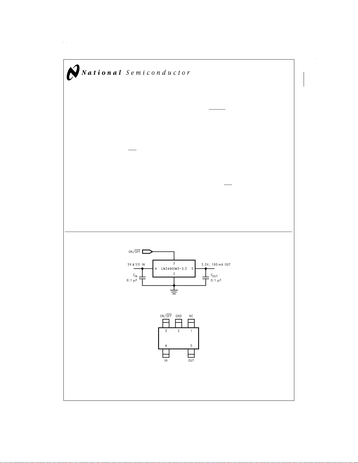
The LM3490 is an integrated linear voltage regulator. It features operation from an input as high as 30V and a guaranteed maximumdropout of 1.2V at the full 100 mA load. Standard packaging for the LM3490 is the 5-lead SOT-23
package. A logic-controlled ON/OFF feature makes the
LM3490 ideal for powering subsystems ON and OFF as
needed.
The 5, 12, and 15V members of the LM3490 series are intended as tiny alternatives to industry standard LM78LXX
series and similar devices. The 1.2V quasi low dropout of
LM3490 series devices makes them a nice fit in many applications where the 2 to 2.5V dropout of LM78LXX series devices precludes their (LM78LXX series devices) use.
The LM3490 series features a 3.3V member. The SOT packaging and quasi low dropout features of the LM3490 series
converge in this device to provide a very nice, very tiny 3.3V,
100 mA bias supply that regulates directly off the system
±
5V
5%power supply.
Typical Application Circuit
Key Specifications
n 30V maximum input for operation
n 1.2V guaranteed maximum dropout over full load and
temperature ranges
n 100 mA guaranteed load current
±
n
5%guaranteed output voltage tolerance over full load
and temperature ranges
n −40 to +125˚C junction temperature range for operation
Features
n 3.3, 5, 12, and 15V versions available
n Logic-controlled ON/OFF
n Packaged in the tiny 5-lead SOT-23 package
Applications
n Tiny alternative to LM78LXX series and similar devices
n Tiny 5V
n Post regulator for switching DC/DC converter
n Bias supply for analog circuits
±
5%to 3.3V, 100 mA converter
DS100071-2
Connection Diagram
DS100071-1
Top View
5-Lead, Molded-Plastic Small-Outline Transistor (SOT) Package
© 1999 National Semiconductor Corporation DS100071 www.national.com
SOT-23 Package
Package Code MA05B(Note 1)
Page 2
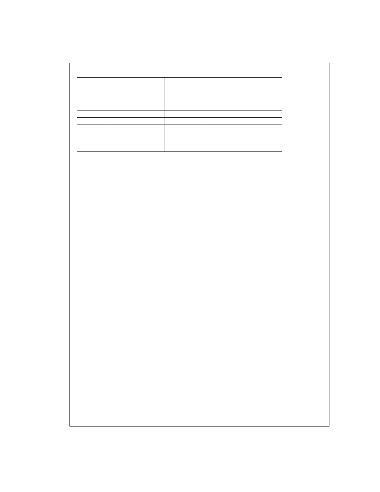
Ordering Information
Output
Voltage
(V)
3.3 LM3490IM5-3.3 L78B 250 Units on Tape and Reel
3.3 LM3490IM5X-3.3 L78B 3k Units on Tape and Reel
5 LM3490IM5-5.0 L79B 250 Units on Tape and Reel
5 LM3490IM5X-5.0 L79B 3k Units on Tape and Reel
12 LM3490IM5-12 L80B 250 Units on Tape and Reel
12 LM3490IM5X-12 L80B 3k Units on Tape and Reel
15 LM3490IM5-15 L81B 250 Units on Tape and Reel
15 LM3490IM5X-15 L81B 3k Units on Tape and Reel
Order
Number
(Note 2)
Package
Marking
(Note 3)
Comments
www.national.com 2
Page 3
Absolute Maximum Ratings (Note 4)
If Military/Aerospace specified devices are required,
please contact the National Semiconductor Sales Office/
ESD (Note 7)
ON/OFF
All Other Pins
Distributors for availability and specifications.
Input Voltage (IN to GND) 35V
Voltage ON/OFF to GND
5.5V
Power Dissipation (Note 5) 400 mW
Junction Temp. (T
) (Note 5) +150˚C
J
Ambient Storage Temp. −65 to +150˚C
Operating Ratings (Note 4)
Maximum Input Voltage (IN to GND) 30V
Voltage ON/OFF to GND
Junction Temperature (T
Maximum Power Dissipation (Note 8) 300 mW
) −40 to +125˚C
J
Soldering Time, Temp. (Note 6)
Wave
Infrared
Vapor Phase
4sec., 260˚C
10sec., 240˚C
75sec., 219˚C
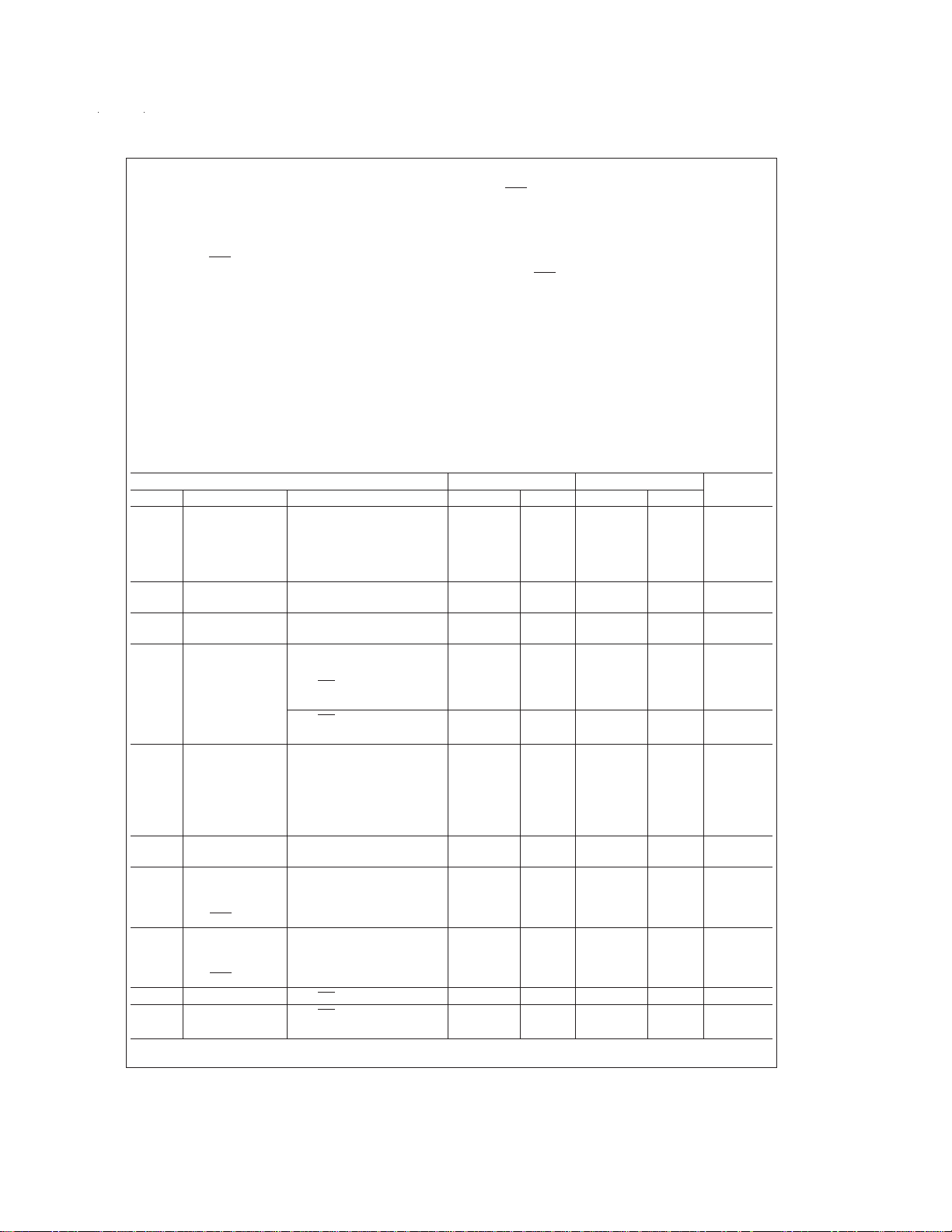
Electrical Characteristics
LM3490-3.3, LM3490-5.0
=
V
IN
pearing in boldface type apply over the entire junction temperature range for operation, −40 to +125˚C. (Notes 9, 10, 11)
+ 1.5V unless otherwise noted. Typicals and limits appearing in normal type apply for T
V
NOM
Nominal Output Voltage (V
) 3.3V 5.0V
NOM
Symbol Parameter Conditions Typical Limit Typical Limit
V
OUT
Output Voltage 1 mA ≤ I
≤ 100 mA 3.30
OUT
3.17
3.14
3.43
3.46
∆V
∆V
I
GND
Line Regulation V
OUT
Load Regulation 10 mA ≤ I
OUT
Ground Pin
Current
+ 1.5V ≤ VIN≤ 30V,
NOM
=
1mA
I
OUT
OUT
V
+ 1.5V ≤ VIN≤ 30V,
NOM
No Load
=
V
ON/OFF
5V
≤ 100 mA 15
7
25
40
22mA
44mA(max)
=
V
ON/OFF
0V
0.1 0.1 µA
55µA(max)
V
-
IN
V
OUT
Dropout Voltage I
=
10 mA 0.7
OUT
=
100 mA 0.9
I
OUT
0.9
1.0
1.1
1.2
e
n
V
IL
Output Noise
Voltage
Maximum Low
Level Input
=
V
10V,
IN
Bandwidth: 10 Hz to 100 kHz
100 150 µV
0.2 0.2 V(max)
Voltage at
ON/OFF
V
IH
Minimum High
Level Input
2.0 2.0 V(min)
Voltage at
ON/OFF
=
I
IL
I
IH
V
V
ON/OFF
ON/OFF
0V
=
5V
11µA
−1 −1 µA(max)
20 20 µA(max)
5.00
9
15
0.7
0.9
=
A
=
T
25˚C. Limits ap-
J
4.80
4.75
5.20
5.25
25
40
0.9
1.0
1.1
1.2
1.0kV
2.0kV
0to5V
Units
V
V(min)
V(min)
V(max)
V(max)
mV
mV(max)
mV
mV(max)
V
V(max)
V(max)
V
V(max)
V(max)
rms
www.national.com3
Page 4

LM3490-12, LM3490-15
=
V
IN
pearing in boldface type apply over the entire junction temperature range for operation, −40 to +125˚C. (Notes 9, 10, 11)
+ 1.5V unless otherwise noted. Typicals and limits appearing in normal type apply for T
V
NOM
Nominal Output Voltage (V
) 12V 15V
NOM
Symbol Parameter Conditions Typical Limit Typical Limit
V
OUT
Output Voltage 1 mA ≤ I
≤ 100 mA 12.00
OUT
11.52
11.40
12.48
12.60
∆V
∆V
I
GND
Line Regulation V
OUT
Load Regulation 10 mA ≤ I
OUT
Ground Pin
Current
+ 1.5V ≤ VIN≤ 30V,
NOM
=
1mA
I
OUT
OUT
V
+ 1.5V ≤ VIN≤ 30V,
NOM
No Load
=
V
ON/OFF
5V
≤ 100 mA 36
14
40
60
22mA
44mA(max)
=
V
ON/OFF
0V
0.1 0.1 µA
55µA(max)
V
-
IN
V
OUT
Dropout Voltage I
=
10 mA 0.7
OUT
=
100 mA 0.9
I
OUT
0.9
1.0
1.1
1.2
e
n
V
IL
Output Noise
Voltage
Maximum Low
Level Input
=
V
10V,
IN
Bandwidth: 10 Hz to 100 kHz
360 450 µV
0.2 0.2 V(max)
Voltage at
ON/OFF
V
IH
Minimum High
Level Input
2.0 2.0 V(min)
Voltage at
ON/OFF
=
I
IL
I
IH
V
V
ON/OFF
ON/OFF
0V
=
5V
11µA
−1 −1 µA(max)
20 20 µA(max)
Note 1: The package code MA05B is internal to National Semiconductor Corporation and indicates a specific version of the SOT-23 package and associated me-
chanical drawings.
Note 2: The suffix “I” indicates the junction temperature range for operation is the industrial temperature range, −40 to +125˚C. The suffix “M5” indicates the die is
packaged in the 5-lead SOT-23 package. The suffix “X” indicates the devices will be supplied in blocks of 3k units as opposed to blocks of 250 units.
Note 3: Because the entire part number does not fit on the SOT-23 package, the SOT-23 package is marked with this code instead of the part number.
Note 4: Absolute Maximum Ratings are limits beyond which damage to the device may occur. Operating Ratings are conditions under which operation of the device
is guaranteed. Operating Ratings do not imply guaranteed performance limits. For guaranteed performance limits and associated test conditions, see the Electrical
Characteristics tables.
Note 5: The Absolute Maximum power dissipation depends on the ambient temperature and can be calculated using P=(T
perature, T
junction temperature, 150˚C, forT
dissipated at higher ambient temperatures. The Absolute Maximum power dissipation can be increased by 4 mW for each ˚C below 50˚C ambient. It must be derated
by 4 mW for each ˚C above 50˚C ambient. A θ
ing enables the safe dissipation of more power. The LM3490 actively limits its junction temperature to about 150˚C.
Note 6: Times shown are dwell times. Temperaturesshown are dwell temperatures. For detailed information on soldering plastic small-outline packages, refer to the
Packaging Databook
Note 7: For testing purposes, ESD was applied using the human-body model, a 100 pF capacitor discharged through a 1.5 kΩ resistor.
Note 8: As with the Absolute Maximum power dissipation, the maximum power dissipation for operation depends on the ambient temperature. The 300 mW rating
appearing under Operating Ratings results from substituting the maximum junction temperature for operation, 125˚C, for T
P=(T
dissipation for operation appearing under Operating Ratings can be increased by 4 mW for each ˚C below 50˚C ambient. It must be derated by 4 mW for each ˚C
above 50˚C ambient. A θ
sipation of more power during operation.
is the ambient temperature, and θJAis the junction-to-ambient thermal resistance. The 400 mW rating results from substituting the Absolute Maximum
A
available from National Semiconductor Corporation.
)/θJA. More power can be dissipated at lower ambient temperatures. Less power can be dissipated at higher ambient temperatures. The maximum power
J−TA
, 50˚C forTA, and 250˚C/W forθJA. More power canbesafelydissipatedatlowerambienttemperatures.Less power can be safely
J
of 250˚C/W represents the worst-case condition of no heat sinking of the 5-lead plastic SOT-23 package. Heat sink-
JA
of 250˚C/W represents the worst-case condition of no heat sinking of the 5-lead plastic SOT-23 package. Heat sinking enables the dis-
JA
=
=
T
A
25˚C. Limits ap-
J
15.00
14.40
14.25
15.60
15.75
16
40
45
75
0.7
0.9
1.0
0.9
1.1
1.2
)/θJAwhere TJis the junction tem-
J-TA
, 50˚C for TA, and 250˚C/W for θJAin
J
Units
V(min)
V(min)
V(max)
V(max)
mV
mV(max)
mV
mV(max)
V(max)
V(max)
V(max)
V(max)
V
V
V
rms
www.national.com 4
Page 5

LM3490-12, LM3490-15 (Continued)
=
Note 9: A typical is the center of characterization data taken with T
Note 10: All limits are guaranteed. All electrical characteristics having room-temperature limits are tested during production with T
its are guaranteed by correlating the electrical characteristics to process and temperature variations and applying statistical process control.
Note 11: All voltages except dropout are with respect to the voltage at the GND pin.
=
T
25˚C. Typicals are not guaranteed.
A
J
=
=
T
25˚C.All hot and cold lim-
A
J
www.national.com5
Page 6

Typical Performance Characteristics Unless indicated otherwise, V
=
C
0.1 µF, and T
OUT
Dropout Voltage
vs Load Current
=
25˚C.
A.
Dropout Voltage
vs Junction Temperature
=
+ 1.5V, C
V
IN
NOM
=
0.1 µF,
IN
Ground Pin Current
vs Input Voltage
Ground Pin Current
vs Load Current
DS100071-19
DS100071-9
DS100071-20
Ground Pin Current
vs Input Voltage
DS100071-10
Ground Pin Current
vs Junction Temperature
DS100071-21
www.national.com 6
DS100071-22
Page 7

Typical Performance Characteristics Unless indicated otherwise, V
C
OUT
=
0.1 µF, and T
=
25˚C. (Continued)
A.
=
+ 1.5V, C
V
IN
NOM
=
0.1 µF,
IN
Input Current
vs Input Voltage
Line Transient Response
DS100071-11
Input Current
vs Input Voltage
DS100071-12
Line Transient Response
Load Transient Response
DS100071-3
DS100071-5
DS100071-4
Load Transient Response
DS100071-6
www.national.com7
Page 8

Typical Performance Characteristics Unless indicated otherwise, V
C
OUT
=
0.1 µF, and T
=
25˚C. (Continued)
A.
=
+ 1.5V, C
V
IN
NOM
=
0.1 µF,
IN
Load Transient Response
Output Voltage
vs Input Voltage
DS100071-7
Load Transient Response
DS100071-8
Output Voltage
vs Input Voltage
DS100071-13
Output Voltage
vs Input Voltage
DS100071-15
www.national.com 8
DS100071-14
Output Voltage
vs Input Voltage
DS100071-16
Page 9

Typical Performance Characteristics Unless indicated otherwise, V
C
OUT
=
0.1 µF, and T
=
25˚C. (Continued)
A.
=
+ 1.5V, C
V
IN
NOM
=
0.1 µF,
IN
Output ShortCircuit Current
Power Supply
Rejection Ratio
DS100071-17
Output ShortCircuit Current
DS100071-18
Power Supply
Rejection Ratio
DC Load
Regulation
DS100071-24
DS100071-23
DS100071-25
www.national.com9
Page 10

Physical Dimensions inches (millimeters) unless otherwise noted
ON/OFF
5-Lead Small-Outline Package (M5)
SOT-23 Package
For Ordering, Refer to Ordering Information Table
NS Package Number MA05B
LIFE SUPPORT POLICY
NATIONAL’S PRODUCTS ARE NOT AUTHORIZED FOR USE AS CRITICAL COMPONENTS IN LIFE SUPPORT
DEVICES OR SYSTEMS WITHOUT THE EXPRESS WRITTEN APPROVAL OF THE PRESIDENT AND GENERAL
COUNSEL OF NATIONAL SEMICONDUCTOR CORPORATION. As used herein:
1. Life support devices or systems are devices or
systems which, (a) are intended for surgical implant
into the body, or (b) support or sustain life, and
whose failure to perform when properly used in
accordance with instructions for use provided in the
2. A critical component is any component of a life
support device or system whose failure to perform
can be reasonably expected to cause the failure of
the life support device or system, or to affect its
safety or effectiveness.
labeling, can be reasonably expected to result in a
significant injury to the user.
National Semiconductor
Corporation
Americas
LM3490 100 mA, SOT-23, Quasi Low-Dropout Linear Voltage Regulator with Logic-Controlled
Tel: 1-800-272-9959
Fax: 1-800-737-7018
Email: support@nsc.com
www.national.com
National does not assume any responsibility for use of any circuitry described, no circuit patent licenses are implied and National reserves the right at any time without notice to change said circuitry and specifications.
National Semiconductor
Europe
Fax: +49 (0) 1 80-530 85 86
Email: europe.support@nsc.com
Deutsch Tel: +49 (0) 1 80-530 85 85
English Tel: +49 (0) 1 80-532 78 32
Français Tel: +49 (0) 1 80-532 93 58
Italiano Tel: +49 (0) 1 80-534 16 80
National Semiconductor
Asia Pacific Customer
Response Group
Tel: 65-2544466
Fax: 65-2504466
Email: sea.support@nsc.com
National Semiconductor
Japan Ltd.
Tel: 81-3-5639-7560
Fax: 81-3-5639-7507
 Loading...