

Datasheet LM348N, LM348D, LM348, LM248D, LM248 Datasheet (SGS Thomson Microelectronics)
...Page 1
QUAD BIPOLAR OPERATIONAL AMPLIFIERS
.LOWSUPPLYCURRENT:0.53mA/AMPLIFIER
.CLASS AB OUTPUT STAGE : NO CROSS-
OVERDISTORTION
.PINCOMPATIBLEWITH LM124
.LOW INPUTOFFSETVOLTAGE:1mV
.LOW INPUTOFFSETCURRENT : 2nA
.LOW INPUTBIASCURRENT : 30nA
.GAINBANDWIDTHPRODUCT : 1.3MHz
.HIGH DEGREE OF ISOLATION BETWEEN
AMPLIFIERS: 120dB
.OVERLOADPROTECTIONFORINPUTSAND
OUTPUTS
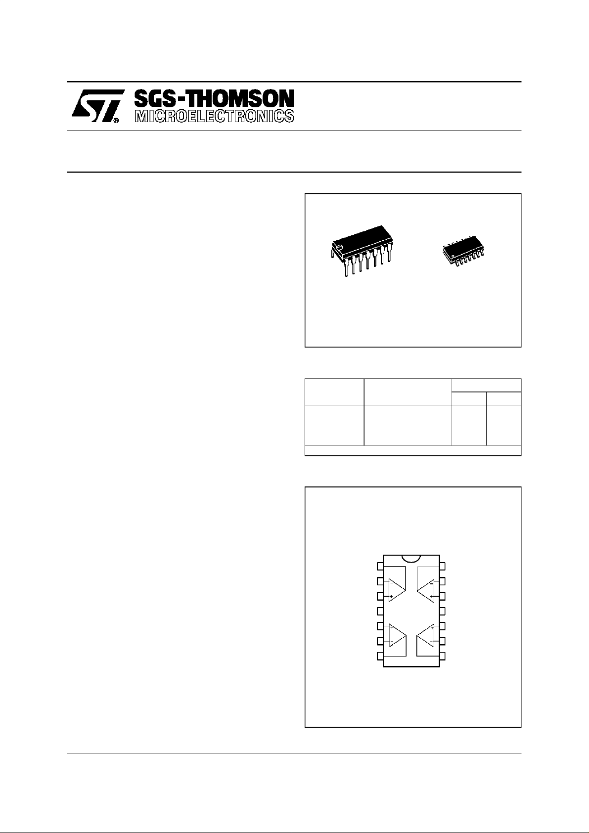
LM24 8 - LM34 8
N
DIP14
(PlasticPackage)
ORDER CODES
LM148
FOURUA741
D
SO14
(PlasticMicropackage)
DESC RIP TI ON
The LM148consistsof four independent,high gain
internally compensated, low power operational
amplifiers which have been designed to provide
functionalcharacteristicsidenticaltothoseofthefamiliar UA741 operational amplifier. In addition the
total supplycurrent forall fouramplifiersis comparable to the supply current of a singleUA741type
op amp. Other featuresincludeinput offsetcurrent
and input bias current which are much less than
thoseof a standardUA741.Also,excellentisolation
between amplifiers has been achieved by independentlybiasing each amplifier and using layout
techniqueswhichminimize thermal coupling.
The LM148can beusedanywheremultipleUA741
type amplifiers are being used and in applications
whereamplifier matchingor highpackingdensityis
required.
Part Num-
ber
LM148 –55
LM248 –40
LM348 0
Example : LM348D
PIN CONNECTIONS (top view)
Outpu t 1
Inve rt ing i npu t 1
Non-inver ting i nput 1
V
CC
Non-inv ert ing input 2
Inve rting input 2
Out put 2
1
2
3
+
4
5
6
7
Temperature
Range
o
C, +125oC ••
o
C, +105oC ••
o
C, +70oC ••
Package
ND
Output 4
14
Inverti ng i npu t 4
13
N on-in ver ting i nput 4
12
-
V
11
CC
10
N on-in ver ting i nput 3
9
Inverting input3
8
Output 3
November 1997
1/9
Page 2
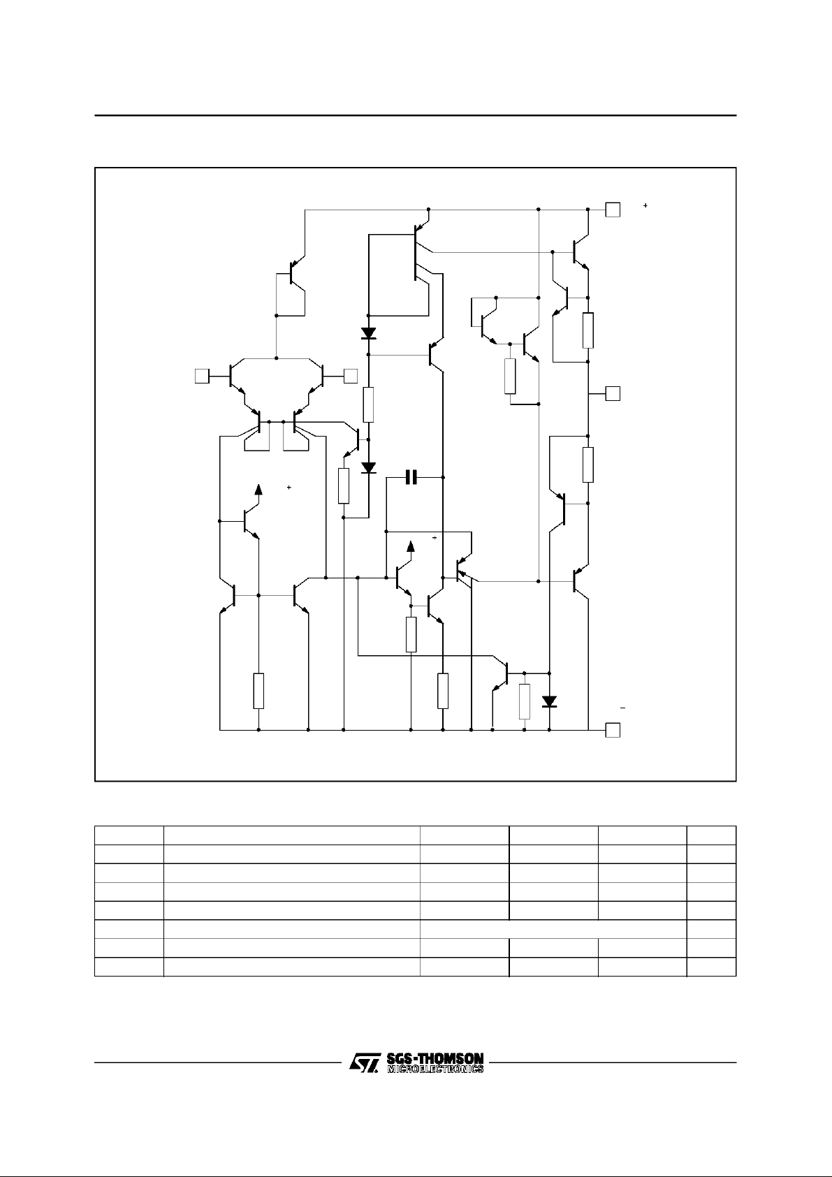
LM148 - LM248 - L M348
SCHE MATIC DIAGRAM
Non-inverting input
Inverting
Input
350k
V
CC
25 Ω
12k Ω
Ω
Output
V
60k
7.4pF
2.5kΩ
CC
V
CC
60k Ω
340 Ω
Ω
36k Ω
Ω
25
V
CC
ABSOLUTE MAXIMUM RATINGS
Symbol Parameter LM148 LM248 LM348 Unit
V
CC
V
V
P
T
oper
T
stg
Notes : 1. For supply voltage less than maximum value, t he absolute maximum input volt age i s equal to the supply
Supply Voltage ± 22 ± 22 ± 22 V
Differential Input Voltage ±44 ± 44 ± 44 V
id
Input Voltage (note 1) ± 22 ± 22 ± 22 V
i
Power Dissipation 500 500 500 mW
tot
Output Short-circuit Duration (note 2) Infinite
Operating Free-air Temperature Range –55, +125 –40, +105 0, +70
Storage Temperature Range –65, +150 –65, +150 –65, +150
voltage.
2. Any of the amplifi er outputs can be shorted to ground indefinitely ; however, more than one s hould not be
simultaneously shorted as the maximum junction temperature will be exceeded.
o
C
o
C
2/9
Page 3
ELECTRICAL CHARACTERISTICS
= ±15V, T
V
CC
Symbol Parameter
V
io
I
io
I
ib
A
vd
SVR Supply Voltage Rejection Ratio (R
I
CC
V
icm
CMR Common Mode Rejection Ratio (R
I
OS
± V
opp
SR Slew Rate (V
t
r
K
OV
R
I
GBP Gain Bandwidth Product (V
THD Total Harmonic Distortion (f = 1kHz, A
e
n
V
o1/Vo2
= 25oC (unless otherwise specified)
amb
Input OffsetVoltage (RS≤ 10kΩ)
=25oC
T
amb
T
min
. ≤ T
amb
≤ T
max.
Input OffsetCurrent
=25oC
T
amb
T
min
. ≤ T
amb
≤ T
max.
Input Bias Current
=25oC
T
amb
T
min
. ≤ T
amb
≤ T
max.
Large Signal Voltage Gain (Vo= ±10V, RL=2kΩ)
=25oC
T
amb
T
T
T
min
amb
min
. ≤ T
. ≤ T
amb
=25oC
amb
≤ T
≤ T
max.
max.
Supply Current, all Amp, no Load
=25oC
T
amb
T
min
. ≤ T
amb
≤ T
max.
Input Common Mode Voltage Range
=25oC
T
amb
T
T
T
min
amb
min
. ≤ T
. ≤ T
amb
=25oC
amb
≤ T
≤ T
max.
max.
Output Short-circuit Current
=25oC 102535
T
amb
Output Voltage Swing
=25oCR
T
amb
. ≤ T
T
min
unity Gain) 0.25 0.5
≤ T
amb
max.
= ±10V, RL= 10kΩ,CL= 100pF,
I
Rise Time (VI= ±10V, RL= 10kΩ,CL= 100pF,
unity Gain) 0.3
Overshoot (VI= ±10V, RL= 10kΩ,CL= 100pF,
unity Gain) 5
Input Resistance 0.8 2.5 MΩ
= 100pF, f = 100kHz) 0.7 1.3
C
L
= 10k
Ω,
R
L
CL= 100pF, Vo=2Vpp) 0.08
I
Equivalent Input Noise Voltage
(f = 1kHz, R
= 100Ω)40
s
Channel Separation 120 dB
≤ 10kΩ)
S
≤ 10kΩ)
S
= 10kΩ
L
=2kΩ
R
L
RL= 10kΩ
=2kΩ
R
L
= 10 mV, RL= 10kΩ,
= 20dB,
v
LM148 - LM248 - LM348
LM148 - LM248 - LM348
Min. Typ. Max.
50
25
77
77
±12
±12
70
70
12
10
12
10
15
225
30 100
160
100
2.1 3.6
110
13
12
6
75
300
4.8
Unit
mV
nA
nA
V/mV
dB
mA
V
dB
mA
V
V/µs
µs
%
MHz
%
nV
√Hz
3/9
Page 4

LM148 - LM248 - L M348
4/9
Page 5

LM148 - LM248 - LM348
5/9
Page 6

LM148 - LM248 - L M348
6/9
Page 7

TES T CIRCUITS
LM148 - LM248 - LM348
5kΩ
1kΩ
e
I
1/4
LM148
e
O
100Ω
10kΩ
1/4
LM148
(10V peak)
e
Crosstalk = -20 log
V
= 15V
CC
101 x
O
(dB)
e
O
7/9
Page 8

LM148 - LM248 - L M348
PACKAG E MECHANICAL DATA
14 PINS - PLASTI C DIP
Dimensions
Min. Typ. Max. Min. Typ. Max.
Millimeters Inches
a1 0.51 0.020
B 1.39 1.65 0.055 0.065
b 0.5 0.020
b1 0.25 0.010
D 20 0.787
E 8.5 0.335
e 2.54 0.100
e3 15.24 0.600
F 7.1 0.280
i 5.1 0.201
L 3.3 0.130
Z 1.27 2.54 0.050 0.100
PM-DIP14.EPS
DIP14.TBL
8/9
Page 9

PACKAG E MECHANICAL DATA
14 PINS - PL ASTIC MICROPACKAGE (SO)
LM148 - LM248 - LM348
Dimensions
Min. Typ. Max. Min. Typ. Max.
Millimeters Inches
A 1.75 0.069
a1 0.1 0.2 0.004 0.008
a2 1.6 0.063
b 0.35 0.46 0.014 0.018
b1 0.19 0.25 0.007 0.010
C 0.5 0.020
c1 45
o
(typ.)
D 8.55 8.75 0.336 0.334
E 5.8 6.2 0.228 0.244
e 1.27 0.050
e3 7.62 0.300
F 3.8 4.0 0.150 0.157
G 4.6 5.3 0.181 0.208
L 0.5 1.27 0.020 0.050
M 0.68 0.027
S8
Information furnished is believed to be accurate and reliable. However, SGS-THOMSON Microelectronics assumes no responsibility for the consequences of use of such information nor for any infringement of patents or other rights of third parties which
may result from its use. No license is granted by implication or otherwise under any patent or patent rights of SGS-THOMSON
Microelectronics. Specification mentioned in this publication are subject to change without notice. This publication supersedes
and replacesall information previously supplied. SGS-THOMSON Microelectronics products are not authorized for use as critical
components in life support devices or systems without express written approval of SGS-THOMSON Microelectronics.
o
(max.)
PM-SO14.EPS
SO14.TBL
1997 SGS-THOMSON Microelectronics – Printed in Italy – All Rights Reserved
SGS-THOMSON Microelectronics GROUP OF COMPANIES
Australia - Brazil- Canada - China - France - Germany - Hong Kong - Italy - Japan - Korea - Malaysia - Malta - Morocco
The Netherlands - Singapore - Spain - Sweden - Switzerland - Taiwan - Thailand - United Kingdom - U.S.A.
ORDER CODE :
9/9
 Loading...