

Page 1
LM3488
High Efficiency Low-Side N-Channel Controller for
Switching Regulators
±
n
General Description
The LM3488 is a versatile Low-Side N-FET high performance controller for switching regulators. It is suitable for
use in topologies requiring low side FET, such as boost,
flyback, SEPIC, etc. Moreover, the LM3488 can be operated
at extremely high switching frequency in order to reduce the
overall solution size. The switching frequency of LM3488 can
be adjusted to any value between 100kHz and 1MHz by
using a single external resistor or by synchronizing it to an
external clock. Current mode control provides superior bandwidth and transient response, besides cycle-by-cycle current
limiting. Output current can be programmed with a single
external resistor.
The LM3488 has built in features such as thermal shutdown,
short-circuit protection and over voltage protection. Power
saving shutdown mode reduces the total supply current to
5µA and allows power supply sequencing. Internal soft-start
limits the inrush current at start-up.
Key Specifications
n Wide supply voltage range of 2.97V to 40V
n 100kHz to 1MHz Adjustable and Synchronizable clock
frequency
1.5% (over temperature) internal reference
n 5µA shutdown current (over temperature)
Features
n 8-lead Mini-SO8 (MSOP-8) package
n Internal push-pull driver with 1A peak current capability
n Current limit and thermal shutdown
n Frequency compensation optimized with a capacitor and
a resistor
n Internal softstart
n Current Mode Operation
n Undervoltage Lockout with hysteresis
Applications
n Distributed Power Systems
n Notebook, PDA, Digital Camera, and other Portable
Applications
n Offline Power Supplies
n Set-Top Boxes
LM3488 High Efficiency Low-Side N-Channel Controller for Switching Regulators
May 2003
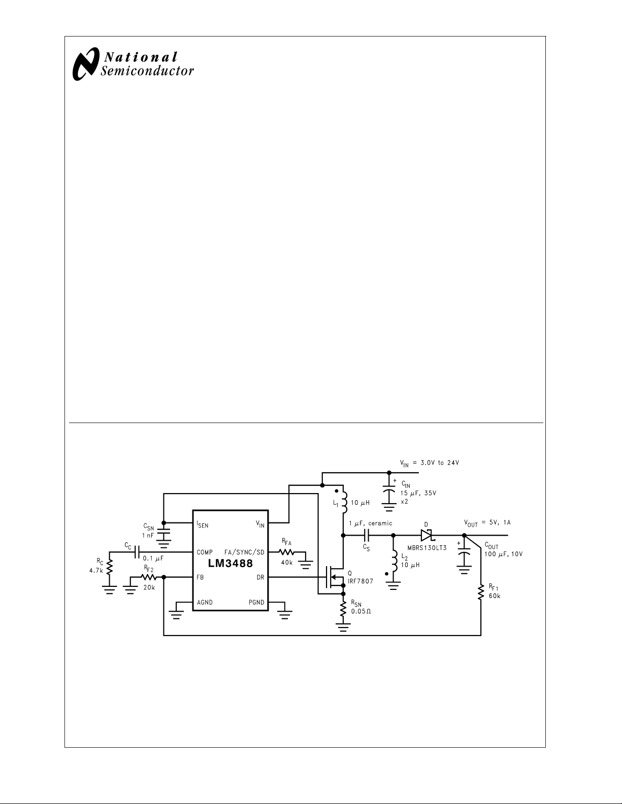
Typical Application Circuit
Typical SEPIC Converter
10138844
© 2003 National Semiconductor Corporation DS101388 www.national.com
Page 2
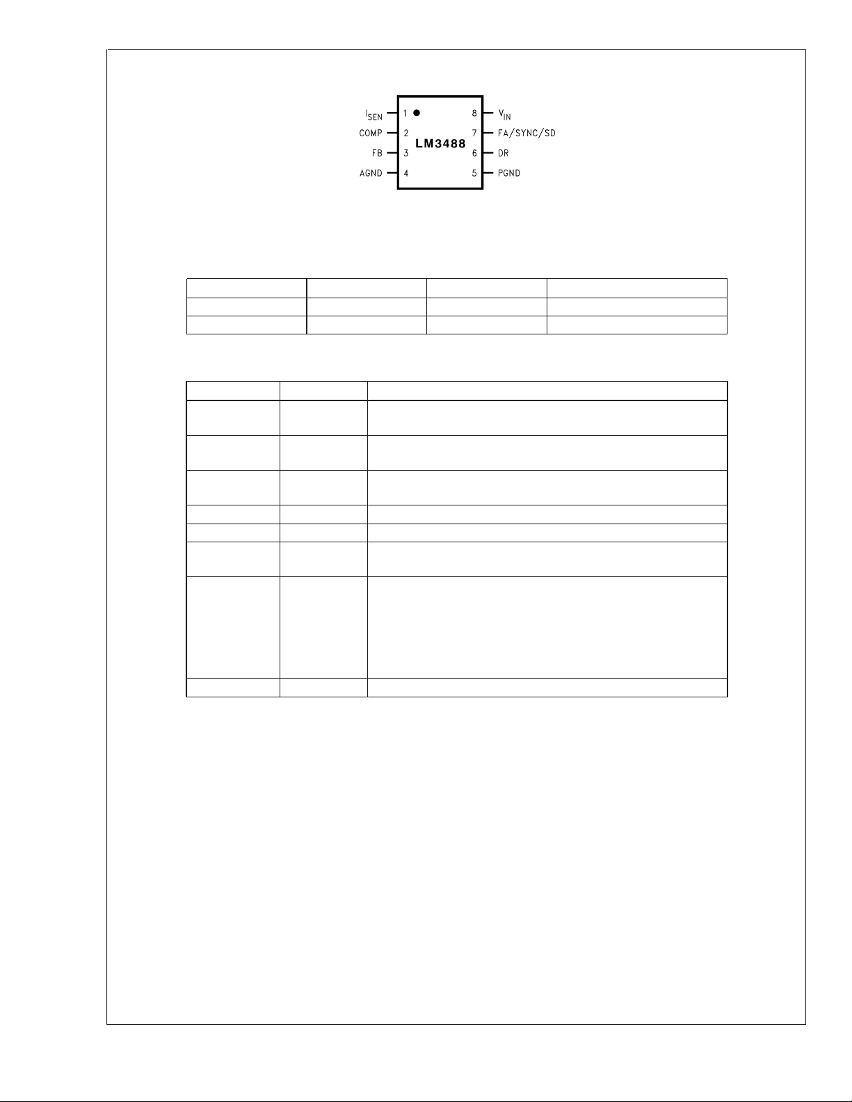
Connection Diagram
LM3488
8 Lead Mini SO8 Package (MSOP-8 Package)
Package Marking and Ordering Information
Order Number Package Type Package Marking Supplied As:
LM3488MM MSOP-8 S21B 1000 units on Tape and Reel
LM3488MMX MSOP-8 S21B 3500 units on Tape and Reel
Pin Description
Pin Name Pin Number Description
I
SEN
COMP 2 Compensation pin. A resistor, capacitor combination connected to
FB 3 Feedback pin. The output voltage should be adjusted using a
AGND 4 Analog ground pin.
PGND 5 Power ground pin.
DR 6 Drive pin of the IC. The gate of the external MOSFET should be
FA/SYNC/SD 7 Frequency adjust, synchronization, and Shutdown pin. A resistor
V
IN
1 Current sense input pin. Voltage generated across an external
sense resistor is fed into this pin.
this pin provides compensation for the control loop.
resistor divider to provide 1.26V at this pin.
connected to this pin.
connected to this pin sets the oscillator frequency. An external
clock signal at this pin will synchronize the controller to the
frequency of the clock. A high level on this pin for ≥ 30µs will turn
the device off. The device will then draw less than 10µA from the
supply.
8 Power supply input pin.
10138802
www.national.com 2
Page 3
LM3488
Absolute Maximum Ratings (Note 1)
If Military/Aerospace specified devices are required,
please contact the National Semiconductor Sales Office/
Distributors for availability and specifications.
Input Voltage 45V
<
<
FA/SYNC/SD
V
FB
<
FB Pin Voltage -0.4V
FA/SYNC/SD Pin Voltage -0.4V
V
Peak Driver Output Current (
<
10µs) 1.0A
Power Dissipation Internally Limited
Storage Temperature Range −65˚C to +150˚C
Junction Temperature +150˚C
ESD Susceptibilty
7V
<
7V
Lead Temperature
MM Package
Vapor Phase (60 sec.)
Infared (15 sec.)
DR Pin Voltage −0.4V ≤ VDR ≤ 8V
I
Pin Voltage 600mV
LIM
Operating Ratings (Note 1)
Supply Voltage 2.97V ≤ V
Junction
Temperature Range −40˚C ≤ TJ≤ +125˚C
Switching Frequency 100kHz ≤ F
SW
IN
≤ 1MHz
Human Body Model (Note 2) 2kV
Electrical Characteristics
Specifications in Standard type face are for TJ= 25˚C, and in bold type face apply over the full Operating Temperature
Range. Unless otherwise specified, V
Symbol Parameter Conditions Typical Limit Units
V
∆V
FB
LINE
Feedback Voltage V
Feedback Voltage
Line Regulation
∆V
LOAD
Output Voltage Load
Regulation
V
UVLO
Input Undervoltage
Lock-out
V
UV(HYS)
Input Undervoltage
Lock-out Hysteresis
F
nom
Nominal Switching
Frequency
R
DS1 (ON)
Driver Switch On
Resistance (top)
R
DS2 (ON)
Driver Switch On
Resistance (bottom)
V
DR (max)
Maximum Drive
Voltage Swing(Note 6)
D
max
Maximum Duty
Cycle(Note 7)
(on) Minimum On Time 325
T
min
I
SUPPLY
Supply Current
(switching)
I
Q
Quiescent Current in
Shutdown Mode
V
SENSE
Current Sense
Threshold Voltage
= 12V, RFA= 40kΩ
IN
COMP
2.97 ≤ V
= 1.4V,
≤ 40V
IN
1.26
1.2507/1.24
1.2753/1.28
2.97 ≤ VIN≤ 40V 0.001 %/V
I
EAO
Source/Sink
±
0.5 %/V (max)
2.85
2.97
170
130
210
RFA= 40KΩ 400
370
420
IDR= 0.2A, VIN=5V 16 Ω
IDR= 0.2A 4.5 Ω
<
V
7.2V V
IN
V
≥ 7.2V 7.2
IN
IN
100 %
230
550
(Note 9)
V
FA/SYNC/SD
10), V
IN
= 5V(Note
=5V
2.0
5
2.6
7
VIN= 5V 165
140/ 135
195/ 200
V(min)
V(max)
V(max)
mV (min)
mV (max)
kHz
kHz(min)
kHz(max)
nsec
nsec(min)
nsec(max)
mA (max)
µA (max)
mV (min)
mV (max)
215˚C
220˚C
≤ 40V
V
V
mV
V
mA
µA
mV
www.national.com3
Page 4
Electrical Characteristics (Continued)
Specifications in Standard type face are for TJ= 25˚C, and in bold type face apply over the full Operating Temperature
LM3488
Range. Unless otherwise specified, V
Symbol Parameter Conditions Typical Limit Units
V
SC
Short-Circuit Current
Limit Sense Voltage
V
SL
Internal Compensation
Ramp Voltage
V
OVP
Output Over-voltage
Protection (with
respect to feedback
voltage) (Note 8)
V
OVP(HYS)
Output Over-Voltage
Protection
Hysteresis(Note 8)
Gm Error Ampifier
Transconductance
A
VOL
Error Amplifier Voltage
Gain
I
EAO
Error Amplifier Output
Current (Source/ Sink)
V
EAO
Error Amplifier Output
Voltage Swing
T
SS
Internal Soft-Start
Delay
T
r
T
f
Drive Pin Rise Time Cgs = 3000pf, VDR=0to
Drive Pin Fall Time Cgs = 3000pf, VDR=0to
VSD Shutdown and
Synchronization signal
threshold (Note 5)
I
SD
Shutdown Pin Current VSD=5V −1 µA
TSD Thermal Shutdown 165 ˚C
T
sh
Thermal Shutdown
Hysteresis
θ
JA
Thermal Resistance MM Package 200 ˚C/W
= 12V, RFA= 40kΩ
IN
VIN= 5V 325
VIN=5V 92
= 1.4V 50
V
COMP
= 1.4V 60
V
COMP
= 1.4V
V
COMP
= 100µA
I
EAO
(Source/Sink)
V
= 1.4V
COMP
= 100µA
I
EAO
(Source/Sink)
Source, V
=0V
V
FB
Sink, V
COMP
COMP
= 1.4V, V
= 1.4V,
FB
= 1.4V
Upper Limit
=0V
V
FB
COMP Pin = Floating
Lower Limit
= 1.4V
V
FB
VFB= 1.2V, V
COMP
=
Floating
3V
3V
Output = High 1.27
Output = Low 0.65
V
=0V +1
SD
235
395
52
132
32/ 25
78/ 85
20
110
800
600/ 365
1000/ 1265
38
26
44
110
80/ 50
140/ 180
−140
−100/ −85
−180/ −185
2.2
1.8
2.4
0.56
0.2
1.0
4 msec
25 ns
25 ns
1.35
0.35
10 ˚C
mV
mV (min)
mV (max)
mV
mV(min)
mV(max)
mV
mV(min)
mV(max)
mV
mV(min)
mV(max)
µmho
µmho (min)
µmho (max)
V/V
V/V (min)
V/V (max)
µA
µA (min)
µA (max)
µA
µA (min)
µA (max)
V
V(min)
V(max)
V
V(min)
V(max)
V
V (max)
V
V (min)
www.national.com 4
Page 5

Electrical Characteristics (Continued)
Note 1: Absolute Maximum Ratings are limits beyond which damage to the device may occur. Operating Ratings are conditions under which operation of the device
is intended to be functional. For guaranteed specifications and test conditions, see the Electrical Characteristics.
Note 2: The human body model is a 100 pF capacitor discharged through a 1.5kΩ resistor into each pin.
Note 3: All limits are guaranteed at room temperature (standard type face) and at temperature extremes (bold type face). All room temperature limits are 100%
tested. All limits at temperature extremes are guaranteed via correlation using standard Statistical Quality Control (SQC) methods. All limits are used to calculate
Average Outgoing Quality Level (AOQL).
Note 4: Typical numbers are at 25˚C and represent the most likely norm.
Note 5: The FA/SYNC/SD pin should be pulled to V
Note 6: The voltage on the drive pin, V
than or equal to 7.2V.
Note 7: The limits for the maximum duty cycle can not be specified since the part does not permit less than 100% maximum duty cycle operation.
Note 8: The over-voltage protection is specified with respect to the feedback voltage. This is because the over-voltage protection tracks the feedback voltage. The
over-voltage thresold can be calculated by adding the feedback voltage, V
Note 9: For this test, the FA/SYNC/SD Pin is pulled to ground using a 40K resistor .
Note 10: For this test, the FA/SYNC/SD Pin is pulled to 5V using a 40K resistor.
is equal to the input voltage when input voltage is less than 7.2V. VDRis equal to 7.2V when the input voltage is greater
DR
through a resistor to turn the regulator off.
IN
to the over-voltage protection specification.
FB
LM3488
www.national.com5
Page 6
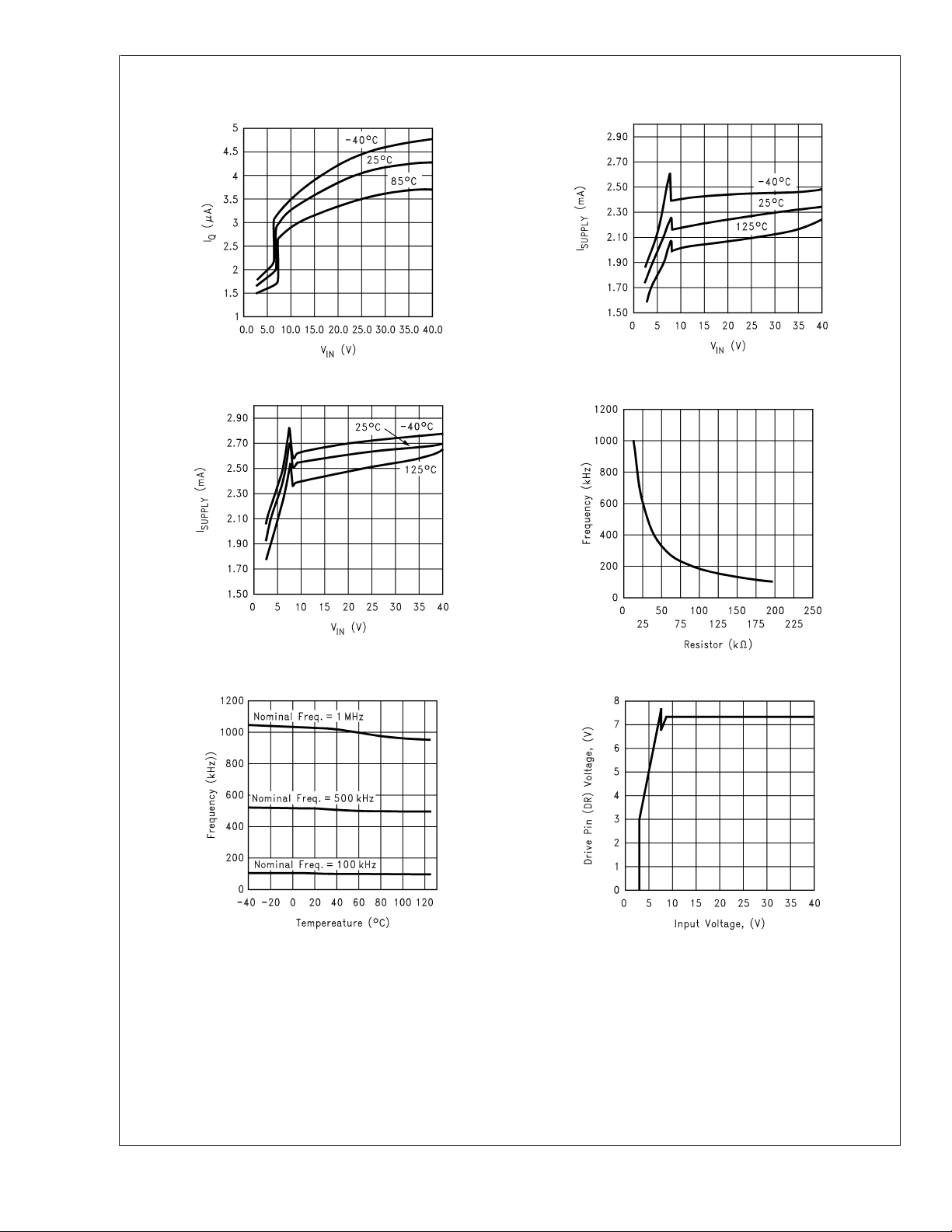
Typical Performance Characteristics Unless otherwise specified, V
LM3488
vs Temperature & Input Voltage I
I
Q
Supply
= 12V, TJ= 25˚C.
IN
vs Input Voltage (Non-Switching)
10138803
I
Supply
vs V
IN
10138835
Switching Frequency vs RFA
Frequency vs Temperature Drive Voltage vs Input Voltage
10138834
10138804
10138854
www.national.com 6
10138805
Page 7
LM3488
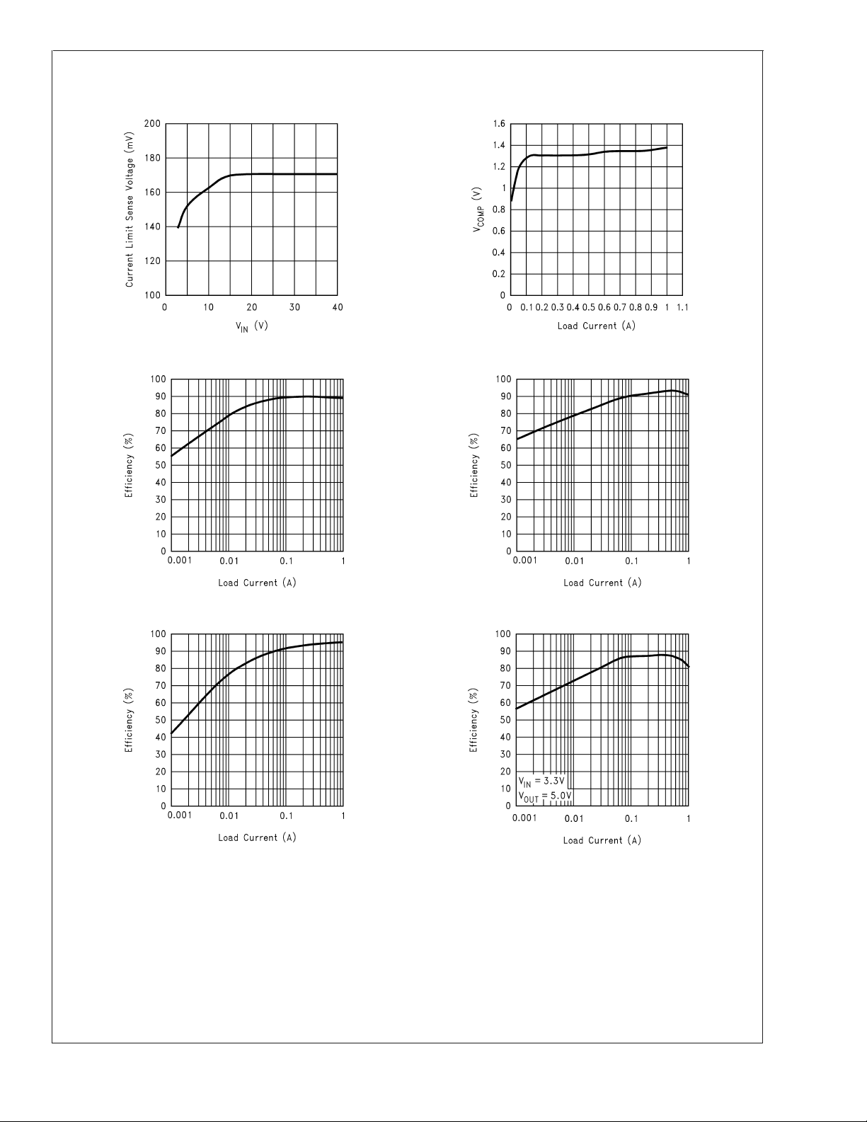
Typical Performance Characteristics Unless otherwise specified, V
= 12V, TJ= 25˚C. (Continued)
IN
Current Sense Threshold vs Input Voltage COMP Pin Voltage vs Load Current
10138845
Efficiency vs Load Current (3.3V In and 12V Out) Efficiency vs Load Current (5V In and 12V Out)
10138862
10138859 10138858
Efficiency vs Load Current (9V In and 12V Out) Efficiency vs Load Current (3.3V In and 5V Out)
10138860
10138853
www.national.com7
Page 8
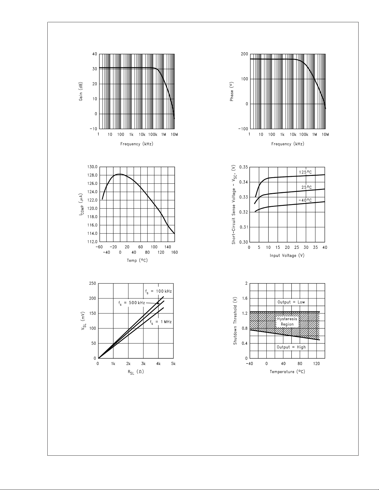
Typical Performance Characteristics Unless otherwise specified, V
LM3488
COMP Pin Source Current vs Temperature Short Circuit Protection vs Input Voltage
Error Amplifier Gain Error Amplifier Phase
10138855 10138856
= 12V, TJ= 25˚C. (Continued)
IN
10138836
10138857
Compensation Ramp vs Compensation Resistor Shutdown Threshold Hysteresis vs Temperature
10138851
10138846
www.national.com 8
Page 9

LM3488
Typical Performance Characteristics Unless otherwise specified, V
Current Sense Voltage vs Duty Cycle
10138852
= 12V, TJ= 25˚C. (Continued)
IN
www.national.com9
Page 10

Functional Block Diagram
LM3488
Functional Description
The LM3488 uses a fixed frequency, Pulse Width Modulated
(PWM), current mode control architecture. In a typical application circuit, the peak current through the external MOSFET is sensed through an external sense resistor. The voltage across this resistor is fed into the I
is then level shifted and fed into the positive input of the
PWM comparator. The output voltage is also sensed through
an external feedback resistor divider network and fed into
the error amplifier negative input (feedback pin, FB). The
output of the error amplifier (COMP pin) is added to the slope
compensation ramp and fed into the negative input of the
PWM comparator.
At the start of any switching cycle, the oscillator sets the RS
latch using the SET/Blank-out and switch logic blocks. This
forces a high signal on the DR pin (gate of the external
MOSFET) and the external MOSFET turns on. When the
voltage on the positive input of the PWM comparator exceeds the negative input, the RS latch is reset and the
external MOSFET turns off.
pin. This voltage
SEN
10138806
The voltage sensed across the sense resistor generally
contains spurious noise spikes, as shown in Figure 1. These
spikes can force the PWM comparator to reset the RS latch
prematurely. To prevent these spikes from resetting the
latch, a blank-out circuit inside the IC prevents the PWM
comparator from resetting the latch for a short duration after
the latch is set. This duration is about 150ns and is called the
blank-out time.
Under extremely light load or no-load conditions, the energy
delivered to the output capacitor when the external MOSFET
is on during the blank-out time is more than what is delivered
to the load. An over-voltage comparator inside the LM3488
prevents the output voltage from rising under these conditions. The over-voltage comparator senses the feedback (FB
pin) voltage and resets the RS latch under these conditions.
The latch remains in reset state till the output decays to the
nominal value.
www.national.com 10
Page 11

Functional Description (Continued)
FIGURE 1. Basic Operation of the PWM comparator
LM3488
10138807
SLOPE COMPENSATION RAMP
The LM3488 uses a current mode control scheme. The main
advantages of current mode control are inherent cycle-bycycle current limit for the switch, and simpler control loop
characteristics. It is also easy to parallel power stages using
current mode control since as current sharing is automatic.
Current mode control has an inherent instability for duty
cycles greater than 50%, as shown in Figure 2.InFigure 2,
a small increase in the load current causes the switch current to increase by ∆I
. The effect of this load change, ∆I1,is
O
:
From the above equation, when D>0.5, ∆I1will be greater
than ∆I
. In other words, the disturbance is divergent. So a
O
very small perturbation in the load will cause the disturbance
to increase.
To prevent the sub-harmonic oscillations, a compensation
ramp is added to the control signal, as shown in Figure 3.
With the compensation ramp,
FIGURE 2. Sub-Harmonic Oscillation for D>0.5
10138809
www.national.com11
Page 12

Functional Description (Continued)
LM3488
FIGURE 3. Compensation Ramp Avoids Sub-Harmonic Oscillation
The compensation ramp has been added internally in
LM3488. The slope of this compensation ramp has been
selected to satisfy most of the applications. The slope of the
internal compensation ramp depends on the frequency. This
slope can be calculated using the formula:
M
C=VSL.FS
In the above equation, V
compensation ramp. Limits for V
the electrical characteristics.
In order to provide the user additional flexibility, a patented
scheme has been implemented inside the IC to increase the
slope of the compensation ramp externally, if the need
arises. Adding a single external resistor, R
Figure 4) increases the slope of the compensation ramp, M
by :
Volts/second
is the amplitude of the internal
SL
have been specified in
SL
SL
(as shown in
10138811
In this equation, ∆VSLis equal to 40.10-6RSL. Hence,
∆VSLversus RSLhas been plotted in Figure 5 for different
frequencies.
C
www.national.com 12
Page 13

Functional Description (Continued)
LM3488
FIGURE 4. Increasing the Slope of the Compensation Ramp
FIGURE 5. ∆VSLvs R
FREQUENCY ADJUST/SYNCHRONIZATION/SHUTDOWN
The switching frequency of LM3488 can be adjusted between 100kHz and 1MHz using a single external resistor.
This resistor must be connected between FA/SYNC/SD pin
and ground, as shown in Figure 6. Please refer to the typical
performance characteristics to determine the value of the
resistor required for a desired switching frequency.
The LM3488 can be synchronized to an external clock. The
external clock must be connected to the FA/SYNC/SD pin
through a resistor, R
as shown in Figure 7. The value of
SYNC
10138813
10138851
SL
this resistor is dependent on the off time of the synchronization pulse, T
OFF(SYNC)
to be used for a given T
. Table 1 shows the range of resistors
OFF(SYNC)
.
TABLE 1.
T
OFF(SYNC)
(µsec) R
SYNC
range (kΩ)
1 5 to 13
2 20to40
3 40to65
www.national.com13
Page 14

Functional Description (Continued)
LM3488
T
OFF(SYNC)
It is also necessary to have the width of the synchronization
pulse narrower than the duty cycle of the converter. It is also
necessary to have the synchronization pulse width ≥
300nsecs.
TABLE 1. (Continued)
(µsec) R
SYNC
range (kΩ)
4 55to90
5 70to110
6 85to140
7 100 to 160
8 120 to 190
9 135 to 215
10 150 to 240
The FA/SYNC/SD pin also functions as a shutdown pin. If a
high signal (refer to the electrical characteristics for definition
of high signal) appears on the FA/SYNC/SD pin, the LM3488
stops switching and goes into a low current mode. The total
supply current of the IC reduces to less than 10µA under
these conditions.
Figure 8 and Figure 9 show implementation of shutdown
function when operating in Frequency adjust mode and synchronization mode respectively. In frequency adjust mode,
connecting the FA/SYNC/SD pin to ground forces the clock
to run at a certain frequency. Pulling this pin high shuts down
the IC. In frequency adjust or synchronization mode, a high
signal for more than 30ms shuts down the IC.
FIGURE 6. Frequency Adjust
FIGURE 7. Frequency Synchronization
10138816
10138815
FIGURE 8. Shutdown Operation in Frequency Adjust Mode
www.national.com 14
10138816
Page 15

Functional Description (Continued)
FIGURE 9. Shutdown Operation in Synchronization Mode
SHORT-CIRCUIT PROTECTION
When the voltage across the sense resistor (measured on
Pin) exceeds 350mV, short-circuit current limit gets
I
SEN
activated. A comparator inside LM3488 reduces the switching frequency by a factor of 5 and maintains this condition till
the short is removed.
Typical Applications
The LM3488 may be operated in either continuous or discontinuous conduction mode. The following applications are
designed for continuous conduction operation. This mode of
operation has higher efficiency and lower EMI characteristics
than the discontinuous mode.
LM3488
10138817
ferred to the load and output capacitor. The ratio of these two
cycles determines the output voltage. The output voltage is
defined as:
BOOST CONVERTER
The most common topology for LM3488 is the boost or
step-up topology. The boost converter converts a low input
voltage into a higher output voltage. The basic configuration
for a boost regulator is shown in Figure 10. In continuous
conduction mode (when the inductor current never reaches
zero at steady state), the boost regulator operates in two
cycles. In the first cycle of operation, MOSFET Q is turned
on and energy is stored in the inductor. During this cycle,
diode D is reverse biased and load current is supplied by the
output capacitor, C
OUT
.
In the second cycle, MOSFET Q is off and the diode is
forward biased. The energy stored in the inductor is trans-
(ignoring the drop across the MOSFET and the diode), or
where D is the duty cycle of the switch, VDis the forward
voltage drop of the diode, and V
is the drop across the
Q
MOSFET when it is on. The following sections describe
selection of components for a boost converter.
www.national.com15
Page 16

Typical Applications (Continued)
LM3488
FIGURE 10. Simplified Boost Converter Diagram (a) First cycle of operation. (b) Second cycle of operation
10138822
POWER INDUCTOR SELECTION
The inductor is one of the two energy storage elements in a
boost converter. Figure 11 shows how the inductor current
varies during a switching cycle. The current through an
inductor is quantified as:
www.national.com 16
10138824
FIGURE 11. A. Inductor current B. Diode current
If VL(t) is constant, diL(t)/dt must be constant. Hence, for a
given input voltage and output voltage, the current in the
inductor changes at a constant rate.
Page 17

Typical Applications (Continued)
The important quantities in determining a proper inductance
value are I
inductor current ripple). If ∆iLis larger than IL, the inductor
current will drop to zero for a portion of the cycle and the
converter will operate in discontinuous conduction mode. If
is smaller than IL, the inductor current will stay above
∆i
L
zero and the converter will operate in continuous conduction
mode. All the analysis in this datasheet assumes operation
in continuous conduction mode. To operate in continuous
conduction mode, the following conditions must be met:
Choose the minimum I
common choice is to set ∆i
appropriate core size for the inductor involves calculating the
average and peak currents expected through the inductor. In
a boost converter,
and I
L_peak=IL
where
(the average inductor current) and ∆iL(the
L
>
∆i
I
L
L
to determine the minimum L. A
OUT
to 30% of IL. Choosing an
L
(max) + ∆iL(max),
PROGRAMMING THE OUTPUT VOLTAGE AND OUTPUT CURRENT
The output voltage can be programmed using a resistor
divider between the output and the feedback pins, as shown
in Figure 12. The resistors are selected such that the voltage
at the feedback pin is 1.26V. R
and RF2can be selected
F1
using the equation,
A 100pF capacitor may be connected between the feedback
and ground pins to reduce noise.
The maximum amount of current that can be delivered at the
output can be controlled by the sense resistor, R
SEN
. Current
limit occurs when the voltage that is generated across the
sense resistor equals the current sense threshold voltage,
V
SENSE
. Limits for V
have been specified in the elec-
SENSE
trical characteristics. This can be expressed as:
*
R
SEN
=V
SENSE
V
I
sw(peak)
represents the maximum value of the control signal
SENSE
as shown in Figure 2. This control signal, however, is not a
constant value and changes over the course of a period as a
result of the internal compensation ramp (see Figure 3).
Therefore the current limit will also change as a result of the
internal compensation ramp. The actual command signal,
, can be better expressed as a function of the sense
V
CS
voltage and the internal compensation ramp:
V
CS=VSENSE
is defined as the internal compensation ramp voltage,
V
SL
−(D*VSL)
limits are specified in the electrical characteristics.
The peak current through the switch is equal to the peak
inductor current.
I
sw(peak)=IL
+ ∆i
L
Therefore for a boost converter
LM3488
A core size with ratings higher than these values should be
chosen. If the core is not properly rated, saturation will
dramatically reduce overall efficiency.
The LM3488 can be set to switch at very high frequencies.
When the switching frequency is high, the converter can be
operated with very small inductor values. With a small inductor value, the peak inductor current can be extremely higher
than the output currents, especially under light load conditions.
The LM3488 senses the peak current through the switch.
The peak current through the switch is the same as the peak
current calculated above.
Combining the three equation yields an expression for R
www.national.com17
SEN
Page 18

Typical Applications (Continued)
LM3488
10138820
FIGURE 12. Adjusting the Output Voltage
CURRENT LIMIT WITH ADDITIONAL SLOPE COMPENSATION
If an external slope compensation resistor is used (see
Figure 4) the internal control signal will be modified and this
will have an effect on the current limit. The control signal is
given by:
V
CS=VSENSE
Where V
and VSLare defined parameters in the elec-
SENSE
trical characteristics section. If R
−(D*VSL)
is used, then this will add
SL
to the existing slope compensation. The command voltage
will then be given by:
V
CS=VSENSE
Where ∆V
and can be calculated by use of Figure 5 or is equal to 40 x
−6
10
is the additional slope compensation generated
SL
*RSL. This changes the equation for R
−(D*(VSL+ ∆VSL))
SEN
to:
Therefore RSLcan be used to provide an additional method
for setting the current limit.
POWER DIODE SELECTION
Observation of the boost converter circuit shows that the
average current through the diode is the average load current, and the peak current through the diode is the peak
current through the inductor. The diode should be rated to
handle more than its peak current. The peak diode current
can be calculated using the formula:
I
D(Peak)=IOUT
/ (1−D) + ∆I
L
In the above equation, I
is the output current and ∆ILhas
OUT
been defined in Figure 11
The peak reverse voltage for boost converter is equal to the
regulator output voltage. The diode must be capable of
handling this voltage. To improve efficiency, a low forward
drop schottky diode is recommended.
POWER MOSFET SELECTION
The drive pin of LM3488 must be connected to the gate of an
external MOSFET. In a boost topology, the drain of the
external N-Channel MOSFET is connected to the inductor
and the source is connected to the ground. The drive pin
(DR) voltage depends on the input voltage (see typical performance characteristics). In most applications, a logic level
MOSFET can be used. For very low input voltages, a sublogic level MOSFET should be used.
The selected MOSFET directly controls the efficiency. The
critical parameters for selection of a MOSFET are:
1. Minimum threshold voltage, V
2. On-resistance, R
3. Total gate charge, Q
DS
(ON)
g
4. Reverse transfer capacitance, C
5. Maximum drain to source voltage, V
TH
(MIN)
RSS
DS(MAX)
The off-state voltage of the MOSFET is approximately equal
to the output voltage. V
DS(MAX)
of the MOSFET must be
greater than the output voltage. The power losses in the
MOSFET can be categorized into conduction losses and ac
switching or transition losses. R
the conduction losses. The conduction loss, P
2
R loss across the MOSFET. The maximum conduction loss
I
is needed to estimate
DS(ON)
COND
,isthe
is given by:
www.national.com 18
Page 19

LM3488
Typical Applications (Continued)
where D
The turn-on and turn-off transitions of a MOSFET require
times of tens of nano-seconds. C
estimate the large instantaneous power loss that occurs
during these transitions.
The amount of gate current required to turn the MOSFET on
can be calculated using the formula:
The required gate drive power to turn the MOSFET on is
equal to the switching frequency times the energy required
to deliver the charge to bring the gate charge voltage to V
(see electrical characteristics and typical performance characteristics for the drive voltage specification).
INPUT CAPACITOR SELECTION
Due to the presence of an inductor at the input of a boost
converter, the input current waveform is continuous and
triangular, as shown in Figure 11. The inductor ensures that
the input capacitor sees fairly low ripple currents. However,
as the input capacitor gets smaller, the input ripple goes up.
The rms current in the input capacitor is given by:
The input capacitor should be capable of handling the rms
current. Although the input capacitor is not as critical in a
boost application, low values can cause impedance interactions. Therefore a good quality capacitor should be chosen
in the range of 100µF to 200µF. If a value lower than 100µF
is used, then problems with impedance interactions or
switching noise can affect the LM3478. To improve performance, especially with V
to use a 20Ω resistor at the input to provide a RC filter. The
resistor is placed in series with the V
capacitor attached to the V
0.1µF or 1µF ceramic capacitor is necessary in this configuration. The bulk input capacitor and inductor will connect on
the other side of the resistor with the input power supply.
is the maximum duty cycle.
MAX
I
G=Qg.FS
P
Drive=FS.Qg.VDR
below 8 volts, it is recommended
IN
IN
and Qgare needed to
RSS
DR
pin with only a bypass
IN
pin directly (see Figure 13). A
OUTPUT CAPACITOR SELECTION
The output capacitor in a boost converter provides all the
output current when the inductor is charging. As a result it
sees very large ripple currents. The output capacitor should
be capable of handling the maximum rms current. The rms
current in the output capacitor is:
Where
and D, the duty cycle is equal to (V
OUT−VIN
)/V
OUT
.
The ESR and ESL of the output capacitor directly control the
output ripple. Use capacitors with low ESR and ESL at the
output for high efficiency and low ripple voltage. Surface
Mount tantalums, surface mount polymer electrolytic and
polymer tantalum, Sanyo- OSCON, or multi-layer ceramic
capacitors are recommended at the output.
Designing SEPIC Using LM3488
Since the LM3488 controls a low-side N-Channel MOSFET,
it can also be used in SEPIC (Single Ended Primary Inductance Converter) applications. An example of SEPIC using
LM3488 is shown in Figure 14. As shown in Figure 14, the
output voltage can be higher or lower than the input voltage.
The SEPIC uses two inductors to step-up or step-down the
input voltage. The inductors L1 and L2 can be two discrete
inductors or two windings of a coupled transformer since
equal voltages are applied across the inductor throughout
the switching cycle. Using two discrete inductors allows use
of catalog magnetics, as opposed to a custom transformer.
The input ripple can be reduced along with size by using the
coupled windings of transformer for L1 and L2.
Due to the presence of the inductor L1 at the input, the
SEPIC inherits all the benefits of a boost converter. One
main advantage of SEPIC over boost converter is the inherent input to output isolation. The capacitor CS isolates the
input from the output and provides protection against
shorted or malfunctioning load. Hence, the A SEPIC is useful
for replacing boost circuits when true shutdown is required.
This means that the output voltage falls to 0V when the
switch is turned off. In a boost converter, the output can only
fall to the input voltage minus a diode drop.
10138893
FIGURE 13. Reducing IC Input Noise
www.national.com19
Page 20

Designing SEPIC Using LM3488
(Continued)
LM3488
The duty cycle of a SEPIC is given by:
In the above equation, VQis the on-state voltage of the
MOSFET, Q, and V
diode.
is the forward voltage drop of the
DIODE
FIGURE 14. Typical SEPIC Converter
POWER MOSFET SELECTION
As in boost converter, the parameters governing the selection of the MOSFET are the minimum threshold voltage,
V
Q
, the on-resistance, R
TH(MIN)
, the reverse transfer capacitance, C
g
mum drain to source voltage, V
, the total gate charge,
DS(ON)
DS(MAX)
, and the maxi-
RSS
. The peak switch
voltage in a SEPIC is given by:
V
SW(PEAK)
=VIN+V
OUT+VDIODE
The selected MOSFET should satisfy the condition:
>
V
DS(MAX)
V
SW(PEAK)
The peak switch current is given by:
The rms current through the switch is given by:
10138844
SELECTION OF INDUCTORS L1 AND L2
Proper selection of the inductors L1 and L2 to maintain
constant current mode requires calculations of the following
parameters.
Average current in the inductors:
I
L2AVE=IOUT
Peak to peak ripple current, to calculate core loss if necessary:
POWER DIODE SELECTION
The Power diode must be selected to handle the peak
current and the peak reverse voltage. In a SEPIC, the diode
peak current is the same as the switch peak current. The
off-state voltage or peak reverse voltage of the diode is V
+V
. Similar to the boost converter, the average diode
OUT
IN
current is equal to the output current. Schottky diodes are
recommended.
www.national.com 20
maintains the condition I
mode.
>
∆iLto ensure constant current
L
Page 21

Designing SEPIC Using LM3488
(Continued)
Peak current in the inductor, to ensure the inductor does not
saturate:
I
must be lower than the maximum current rating set by
L1PK
the current sense resistor.
The value of L1 can be increased above the minimum rec-
ommended to reduce input ripple and output ripple. However, once D
is less than 20% of I
IL1
output ripple is minimal.
By increasing the value of L2 above the minimum recom-
mended, ∆
can be reduced, which in turn will reduce the
IL2
output ripple voltage:
, the benefit to
L1AVE
having high rms current ratings relative to size. Ceramic
capacitors could be used, but the low C values will tend to
cause larger changes in voltage across the capacitor due to
the large currents. High C value ceramics are expensive.
Electrolytics work well for through hole applications where
the size required to meet the rms current rating can be
accommodated. There is an energy balance between CS
and L1, which can be used to determine the value of the
capacitor. The basic energy balance equation is:
Where
is the ripple voltage across the SEPIC capacitor, and
is the ripple current through the inductor L1. The energy
balance equation can be solved to provide a minimum value
:
for C
S
LM3488
where ESR is the effective series resistance of the output
capacitor.
If L1 and L2 are wound on the same core, then L1 = L2 = L.
All the equations above will hold true if the inductance is
replaced by 2L. A good choice for transformer with equal
turns is Coiltronics CTX series Octopack.
SENSE RESISTOR SELECTION
The peak current through the switch, I
SW(PEAK)
justed using the current sense resistor, R
certain output current. Resistor R
can be selected using
SEN
can be ad-
, to provide a
SEN
the formula:
Sepic Capacitor Selection
The selection of SEPIC capacitor, CS, depends on the rms
current. The rms current of the SEPIC capacitor is given by:
The SEPIC capacitor must be rated for a large ACrms current relative to the output power. This property makes the
SEPIC much better suited to lower power applications where
the rms current through the capacitor is relatively small
(relative to capacitor technology). The voltage rating of the
SEPIC capacitor must be greater than the maximum input
voltage. Tantalum capacitors are the best choice for SMT,
Input Capacitor Selection
Similar to a boost converter, the SEPIC has an inductor at
the input. Hence, the input current waveform is continuous
and triangular. The inductor ensures that the input capacitor
sees fairly low ripple currents. However, as the input capacitor gets smaller, the input ripple goes up. The rms current in
the input capacitor is given by:
The input capacitor should be capable of handling the rms
current. Although the input capacitor is not as critical in a
boost application, low values can cause impedance interactions. Therefore a good quality capacitor should be chosen
in the range of 100µF to 200µF. If a value lower than 100µF
is used, then problems with impedance interactions or
switching noise can affect the LM3478. To improve performance, especially with V
below 8 volts, it is recommended
IN
to use a 20Ω resistor at the input to provide a RC filter. The
resistor is placed in series with the V
capacitor attached to the V
pin directly (see Figure 13). A
IN
pin with only a bypass
IN
0.1µF or 1µF ceramic capacitor is necessary in this configuration. The bulk input capacitor and inductor will connect on
the other side of the resistor with the input power supply.
Output Capacitor Selection
The ESR and ESL of the output capacitor directly control the
output ripple. Use low capacitors with low ESR and ESL at
www.national.com21
Page 22

Output Capacitor Selection
(Continued)
LM3488
the output for high efficiency and low ripple voltage. Surface
mount tantalums, surface mount polymer electrolytic and
polymer tantalum, Sanyo- OSCON, or multi-layer ceramic
capacitors are recommended at the output.
The output capacitor of the SEPIC sees very large ripple
currents (similar to the output capacitor of a boost converter.
The rms current through the output capacitor is given by:
The ESR and ESL of the output capacitor directly control the
output ripple. Use low capacitors with low ESR and ESL at
the output for high efficiency and low ripple voltage. Surface
mount tantalums, surface mount polymer electrolytic and
polymer tantalum, Sanyo- OSCON, or multi-layer ceramic
capacitors are recommended at the output for low ripple.
www.national.com 22
Page 23

Other Application Circuits
FIGURE 15. Typical High Efficiency Step-Up (Boost) Converter
LM3488
10138843
www.national.com23
Page 24

Physical Dimensions inches (millimeters)
unless otherwise noted
LIFE SUPPORT POLICY
NATIONAL’S PRODUCTS ARE NOT AUTHORIZED FOR USE AS CRITICAL COMPONENTS IN LIFE SUPPORT
DEVICES OR SYSTEMS WITHOUT THE EXPRESS WRITTEN APPROVAL OF THE PRESIDENT AND GENERAL
COUNSEL OF NATIONAL SEMICONDUCTOR CORPORATION. As used herein:
1. Life support devices or systems are devices or
LM3488 High Efficiency Low-Side N-Channel Controller for Switching Regulators
systems which, (a) are intended for surgical implant
into the body, or (b) support or sustain life, and
whose failure to perform when properly used in
accordance with instructions for use provided in the
2. A critical component is any component of a life
support device or system whose failure to perform
can be reasonably expected to cause the failure of
the life support device or system, or to affect its
safety or effectiveness.
labeling, can be reasonably expected to result in a
significant injury to the user.
National Semiconductor
Americas Customer
Support Center
Email: new.feedback@nsc.com
Tel: 1-800-272-9959
www.national.com
National does not assume any responsibility for use of any circuitry described, no circuit patent licenses are implied and National reserves the right at any time without notice to change said circuitry and specifications.
National Semiconductor
Europe Customer Support Center
Fax: +49 (0) 180-530 85 86
Email: europe.support@nsc.com
Deutsch Tel: +49 (0) 69 9508 6208
English Tel: +44 (0) 870 24 0 2171
Français Tel: +33 (0) 1 41 91 8790
National Semiconductor
Asia Pacific Customer
Support Center
Email: ap.support@nsc.com
National Semiconductor
Japan Customer Support Center
Fax: 81-3-5639-7507
Email: jpn.feedback@nsc.com
Tel: 81-3-5639-7560
 Loading...