

Page 1
LM348/LM248
Quad Operational Amplifier
www.fairchildsemi.com
Features
• LM741 OP Amp operating characteristics
• Low supply current drain
• Class AB output stage no crossover distortion
• Pin compatible with the LM324/LM248
• Low input offset voltage : 1mV Typ.
• Low input offset current : 4nA Typ.
• Low input bias current : 30nA Typ.
• Gain bandwidth (unity gain): 1.0MHz Typ.
• High degree of isolation bet ween amplif iers: 120dB
• Overload protection for inputs and outputs
Description
TheLM348/LM248 is a true quad LM741. It consists of four
independent, high-gain, internally compensated, low power
operational amplifiers which have been designed to provide
functional characteristics identical to those of the familiar
LM741 operational amplifier. In addition the total supply
current for all four amplifiers is comparable to the supply
current of a single LM741 type OP Amp. Other features
include input offset currents and input bias current which are
much less than those of a standard LM741. Also, excellent
isolation between amplifiers has been achieved by
independently biasing each amplifier and using layout
techniques which minimize thermal coupling.
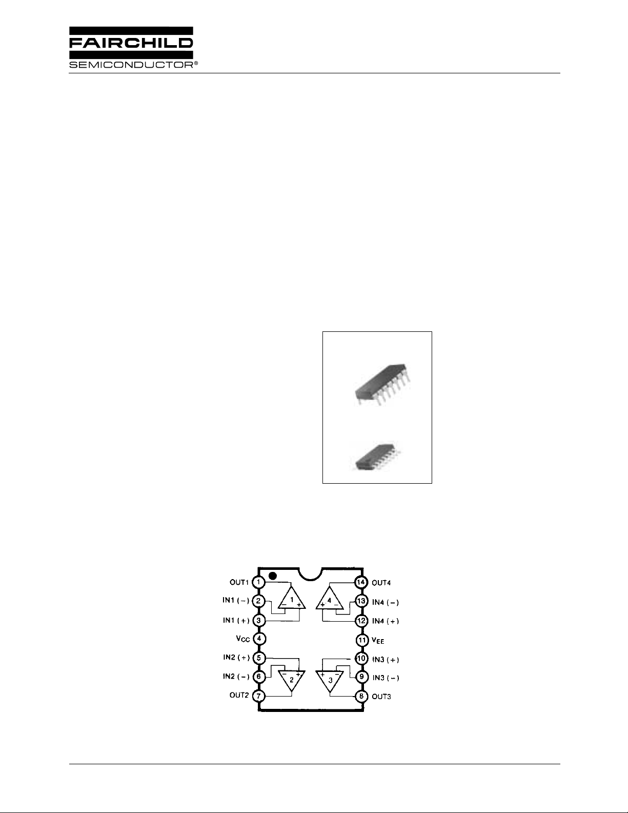
14-DIP
1
14-SOP
1
Internal Block Diagram
©2001 Fairchild Semiconductor Corporation
Rev. 1.0.1
Page 2
LM348/LM248
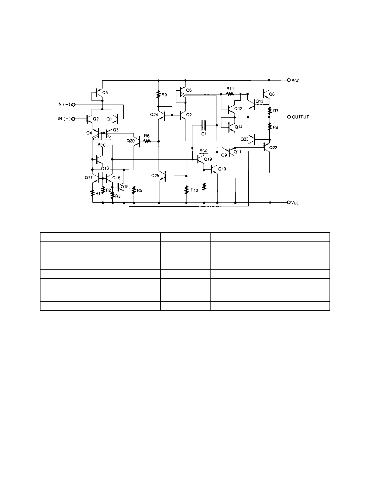
Schematic Diagram
(One Section Only)
Absolute Maximum Ratings
Parameter Symbol Value Unit
Supply Voltage V
Differential Input Voltage V
Input Voltage V
Output Short Circuit Duration - Continuous Operating Temperature
LM348
LM248
Storage Temperature T
CC
I(DIFF)
I
T
OPR
STG
±18 V
36 V
±18 V
0 ~ +70
-25 ~ +85
- 65~ +150 °C
°C
2
Page 3
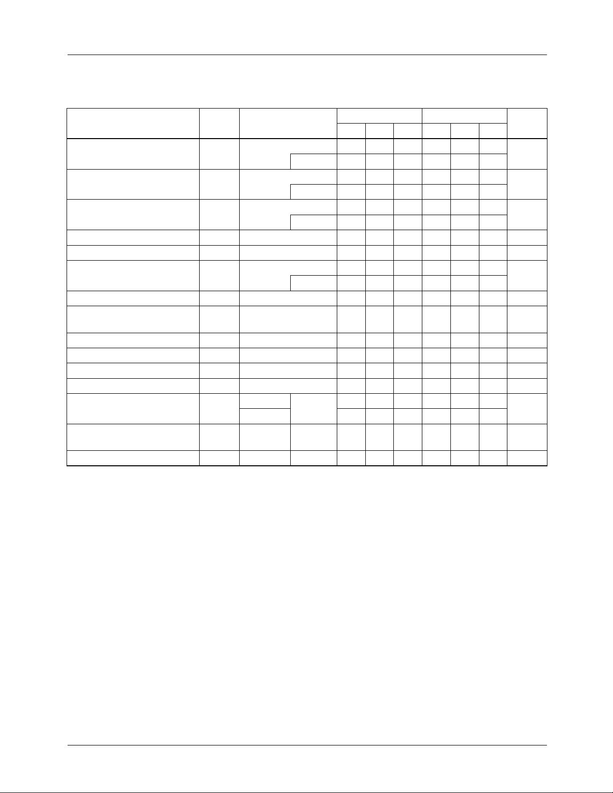
Electrical Characteristics
(VCC =15V, VEE= -15V, TA=25
°C, unless otherwise specified)
LM348/LM248
Parameter Symbol Conditions
Input Offset Voltage V
Input Offset Current I
Input Bias Current I
BIAS
Input Resistance R
Supply Current (all Amplifiers) I
Large Signal Voltage Gain G
IO
IO
CC
R
≤10KΩ -16.0-16.0
S
Note 1 - - 7.5 - - 7.5
Note 1 - - 125 - - 100
Note 1 - - 500 - - 400
I
- 0.8 2.5 - 0.8 2.5 - MΩ
- - 2.4 4.5 - 2.4 4.5 mA
R
≥2KΩ 25 160 - 25 160 -
V
L
Note 115- -15- -
LM248 LM348
Min. Typ. Max. Min. Typ. Max.
- 4 50 - 4 50
- 30 200 - 30 200
Unit
mV
nA
nA
V/mV
Channel Separation CS f = 1KHz to 20KHz - 120 - - 120 - dB
Common Mode Input
Voltage Range
V
Small Signal Bandwidth BW G
Phase Margin (Note2) MPH G
Slew Rate (Note2) SR G
Output Short Circuit Current I
Output Volt ag e Swin g V
Common Mode Rejection
Ratio
SC
O(P-P)
CMRR R
Power Supply Rejection Ratio PSRR R
Note 1 ±12 - - ±12 - - V
I(R)
= 1 - 1.0 - - 1.0 - MHz
V
= 1 - 60 - - 60 - Degree
V
= 1 - 0.5 - - 0.5 - V/µs
V
- - 25 - - 25 - mA
R
≥10KΩ Note 1 ±12 ±13 - ±12 ±13 -
L
≥2KΩ±10 ±12 - ±10 ±12 -
R
L
≥10KΩ Note 1 70 90 - 70 90 - dB
S
≥10KΩ Note 1 77 96 - 77 96 - dB
S
V
Note :
1. LM348: 0 ≤ T
2. Guaranteed by design.
≤ +70
A
°C , LM248: -25 ≤ T
≤ +85
A
°C
3
Page 4

LM348/LM248
Typical Performance Characteristics
Supply Voltage (V) Supply Voltage (V)
Figure 1. Supply Current vs Supply voltage Figure 2. Output Voltage Swing vs Supply voltage
Source Current (mA)
Figure 3. Output voltage swing vs Source Current (mA)
Frequency (Hz) Frequency (Hz)
Figure 5. Output Impedance vs Freque ncy Figure 6. Common-mode Rejection R atio vs Frequency
Figure 4. Output voltage swing vs Sink Current (mA)
Sink Current (mA)
4
Page 5

Typical Performance Characteristics (continued)
Figure 7. Open Loop Frequency Response Figure 8. Bode Plot
LM348/LM248
Figure 9. Large Signal Pulse Response Figure 10. Small Signal Pulse Response
Figure 11. Undistort ed Output Voltag e Sw ing vs Frequency Fi gure 12. Inverting Large Signal Pul se Response
5
Page 6

LM348/LM248
Typical Performance Characteristics (continued)
Figure 13. Input Noise Voltage And Noise Current vs Fre-
quency
Figure 15. Negative Common.mode Input Voltage Limit vs
Negative Supply Voltage
Figure 14. Positive Commo n Mode Input Voltage Limit
vs Positiue Supply Voltage
6
Page 7

Mechanical Dimensions
Package
6.40
±0.20
±0.008
0.252
14-DIP
2.08
0.082
()
LM348/LM248
#1
#7
7.62
0.300
#14
#8
MAX
19.80
0.780
0.128
3.25
±0.20
±0.008
19.40
0.764
±0.20
±0.008
±0.10
0.46
0.20
0.008
±0.004
0.018
2.54
0.100
MIN
±0.10
1.50
±0.004
0.059
0~15°
0.25
0.010
5.08
0.200
+0.10
–0.05
+0.004
–0.002
MAX
3.30
0.130
±0.30
±0.012
7
Page 8

LM348/LM248
Mechanical Dimensions
Package
#1
14-SOP
#14
1.55
0.061
±0.10
±0.004
MIN
0.05
0.002
0.47
0.019
()
0.10
+
-0.05
0.20
0.60
0.024
0.004
+
-0.002
0.008
±0.20
±0.008
#7
6.00
0.236
3.95
0.156
0.225
±0.30
±0.012
±0.20
±0.008
5.72
#8
0~8°
MAX
8.70
0.343
1.80
0.071
±0.20
8.56
MAX
±0.008
0.337
MAX0.10
MAX0.004
0.10
-0.05
+
0.406
0.004
+
1.27
-0.002
0.016
0.050
8
Page 9

Ordering Information
Product Number Package Operating Temperature
LM348N 14-DIP
LM348M 14-SOP
LM248N 14-DIP
LM248M 14-SOP
0 ~ + 70
-25 ~ + 85
o
C
o
C
LM348/LM248
9
Page 10

LM348/LM248
DISCLAIMER
FAIRCHILD SEMICONDUCTOR RESERVES THE RIGHT TO MAKE CHANGES WITHOUT FURT HER NOTICE TO ANY
PRODUCTS HEREI N TO IMPROVE RELIABILITY, FUNCTIO N OR DESIGN. FAIRCH IL D DOES NOT ASSUME ANY
LIABILITY ARISING OUT OF THE APPLICATION OR USE OF ANY PRODUCT OR CIRCUIT DESCRIBED HEREIN; NEITHER
DOES IT CONVEY ANY LICENSE UNDER IT S PATENT RIGHTS, NOR THE RIGHTS OF OTHE RS.
LIFE SUPPORT POL I CY
FAIRCHILD’S PR ODUCTS ARE NOT AUTH ORIZED FOR USE AS C RITICAL COMPONENT S IN LIFE SUPPORT DE VICES
OR SYSTEMS WITHOUT THE EXPRESS WRITTEN APPROVAL OF THE PRESIDENT OF FAIRCHILD SEMICONDUCTOR
CORPORATION. As used herein :
1. Life support devices or systems are devices or systems
which, (a) are intended for surgical implant into the body,
or (b) support or sustain life, and (c) whose failure to
perform when properly used in accordance with
2. A critical component in any component of a life support
device or sy stem whose fai lure to perform can be
reasonably expec ted to cause the failur e of the life support
device or system, or to affect its safety or effec t iv ene ss .
instructions for use provided in the labeling, can be
reasonably expected to result in a significant injury of the
user.
www.fairchildsemi.com
6/1/01 0.0m 001
2001 Fairchild Semiconductor Corporation
Stock#DSxxxxxxxx
 Loading...