

Page 1
LM3477/LM3477A
High Efficiency High-Side N-Channel Controller for
Switching Regulator
General Description
The LM3477/A is a high-side N-channel MOSFET switching
regulator controller. It can be used in topologies requiring a
high side MOSFET such as buck, inverting (buck-boost) and
zeta regulators. The LM3477/A’s internal push pull driver
allows compatibility with a wide range of MOSFETs. This, the
wide input voltage range, use of discrete power components
and adjustable current limit allows the LM3477/A to be optimized for a wide variety of applications.
The LM3477/A uses a high switching frequency of 500kHz to
reduce the overall solution size. Current-mode control requires only a single resistor and capacitor for frequency
compensation. The current mode architecture also yields
superior line and load regulation and cycle-by-cycle current
limiting. A 5µA shutdown state can be used for power savings and for power supply sequencing. Other features include internal soft-start and output over voltage protection.
The internal soft-start reduces inrush current. Over voltage
protection is a safety feature to ensure that the output voltage stays within regulation.
The LM3477A is similar to the LM3477. The primary difference between the two is the point at which the device
transitions into hysteretic mode. The hysteretic threshold of
the LM3477A is one-third of the LM3477.
Features
n 500kHz switching frequency
n Adjustable current limit
n 1.5% reference
n Thermal shutdown
n Frequency compensation optimized with a single
capacitor and resistor
n Internal softstart
n Current mode operation
n Undervoltage lockout with hysteresis
n 8-lead Mini-SO8 (MSOP-8) package
Applications
n Local Voltage Regulation
n Distributed Power
n Notebook and Palmtop Computers
n Internet Appliances
n Printers and Office Automation
n Battery operated Devices
n Cable Modems
n Battery Chargers
Hysteretic
Threshold
LM3477 ) 36% of
programmed current
limit
LM3477A ) 12% of
programmed current
limit
*
See Hysteretic Threshold and section for more information.
LM3477/LM3477A High Efficiency High-Side N-Channel Controller for Switching Regulator
June 2002
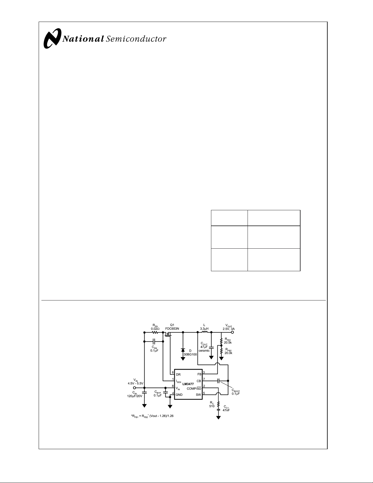
Typical Application Circuit
Typical High Efficiency Step-Down (Buck) Converter
© 2002 National Semiconductor Corporation DS200033 www.national.com
20003333
Page 2
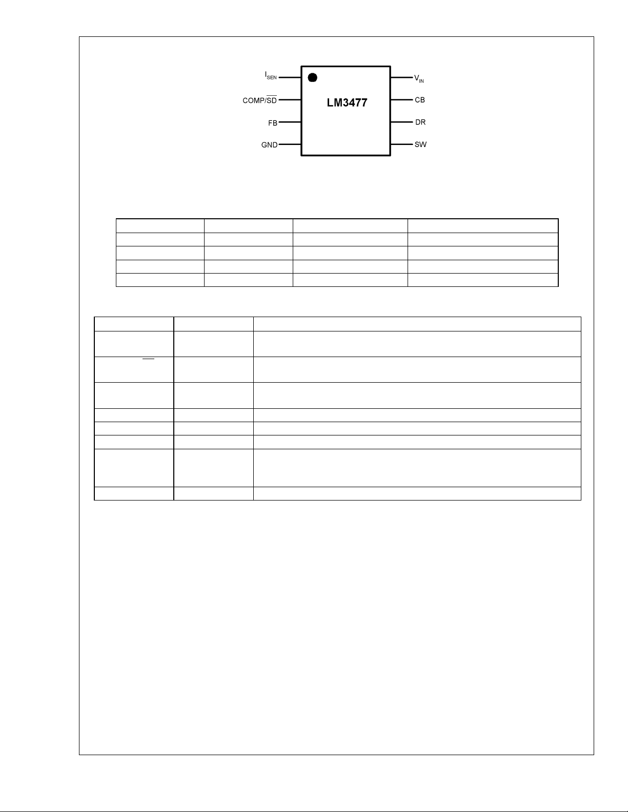
Connection Diagram
LM3477/LM3477A
8 Lead Mini SO8 Package (MSOP-8 Package)
Package Marking and Ordering Information
Order Number Package Type Package Marking Supplied As:
LM3477MM MSOP-8 S13B 1000 units on Tape and Reel
LM3477MMX MSOP-8 S13B 3500 units on Tape and Reel
LM3477AMM MSOP-8 S13A 1000 units on Tape and Reel
LM3477AMMX MSOP-8 S13A 3500 units on Tape and Reel
Pin Description
Pin Name Pin Number Description
I
SEN
COMP/SD
FB 3 Feedback pin. The output voltage should be adjusted using a resistor divider to
GND 4 Ground pin.
SW 5 Switch Node. Source of the external MOSFET is connected to this node.
DR 6 Drive pin. The gate of the external MOSFET should be connected to this pin.
CB 7 Boot-strap pin. A capacitor must be connected between this pin and SW pin (pin 5)
V
IN
1 Current sense input pin. Voltage generated across an external sense resistor is fed
into this pin.
2 Compensation pin. A resistor-capacitor combination connected to this pin provides
compensation for the control loop. Pull this pin below 0.65V to shutdown.
provide 1.270V at this pin.
for proper operation. The voltage developed across this capacitor provides the gate
drive for the external MOSFET.
8 Power Supply Input pin.
20003302
www.national.com 2
Page 3
LM3477/LM3477A
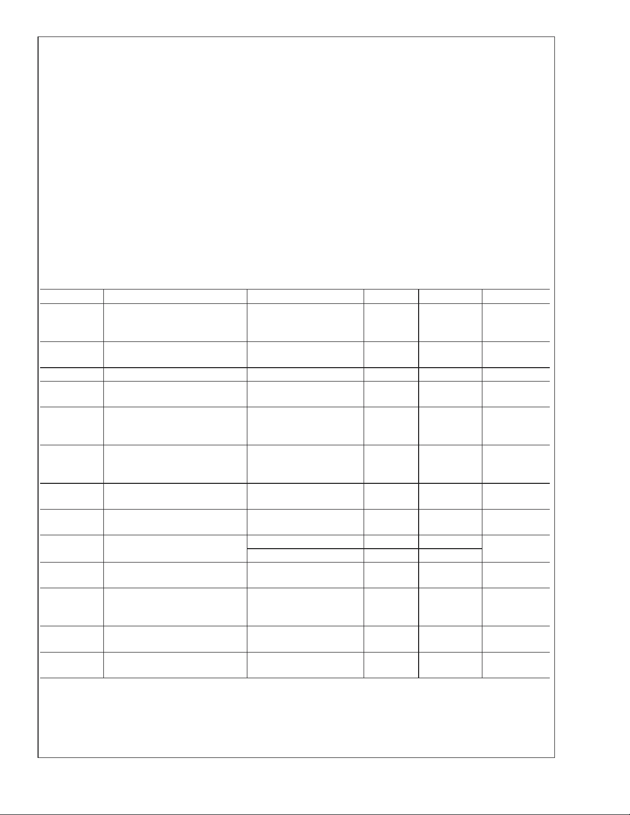
Absolute Maximum Ratings (Note 1)
If Military/Aerospace specified devices are required,
please contact the National Semiconductor Sales Office/
Lead Temperature for MSOP Package
Vapor Phase (60 sec.)
Infared (15 sec.)
Distributors for availability and specifications.
Input Voltage 36V
<
Peak Driver Output Current (
10µs) 1.0A
CB Pin Voltage (Note 2) 43V
I
Pin Voltage 500mV
SEN
Power Dissipation Internally Limited
Operating Ratings (Note 1)
Supply Voltage 2.97V ≤ V
Junction
Temperature Range −40˚C ≤ T
IN
≤ +125˚C
J
Storage Temperature Range −65˚C to +150˚C
Junction Temperature +150˚C
ESD Susceptibilty (Note 3)
Human Body Model
Machine Model
2kV
200V
Electrical Characteristics (Note 4)
Specifications in Standard type face are for TJ= 25˚C, and in bold type face apply over the full Operating Temperature
Range. Unless otherwise specified, V
Symbol Parameter Conditions Typical Limit Units
V
∆V
FB
LINE
Feedback Voltage V
Feedback Voltage Line
Regulation
∆V
V
UVLO
V
UV(HYS)
LOAD
Output Voltage Load Regulation
Input Undervoltage Lock-out 2.87
Input Undervoltage Lock-out
Hysteresis
F
SW
R
DS1 (ON)
Switching Frequency 500
Driver Switch On Resistance
(top)
R
DS2 (ON)
Driver Switch On Resistance
(bottom)
(V
CB−VSW)max
D
max
(on) Minimum On Time 330
T
min
I
SUPPLY
I
Q
Maximum Boot Voltage V
Maximum Duty Cycle 93
Supply Current (switching) (Note 5) 2.0
Quiescent Current in Shutdown
Mode
IN
= 12V.
= 1.4V,
COMP
2.97V ≤ V
IN
≤ 36V
1.270
1.260/1.252
1.288/1.290
V(min)
V(max)
2.97V ≤ VIN≤ 36V 0.001 %/V
±
0.5 %/V (max)
2.97
V(max)
180
130
225
435
575
mV (min)
mV (max)
kHz(min)
kHz(max)
IDR= 0.2A, VIN=5V 7 Ω
IDR= 0.2A 4 Ω
<
7.2V V
IN
V
≥ 7.2V 7.2
IN
IN
88
230
495
3.0
%(min)
nsec(min)
nsec(max)
mA (max)
(Note 6), VIN=5V 5
8
µA (max)
215˚C
220˚C
≤ 35V
V
V
mV
kHz
V
%
nsec
mA
µA
www.national.com3
Page 4
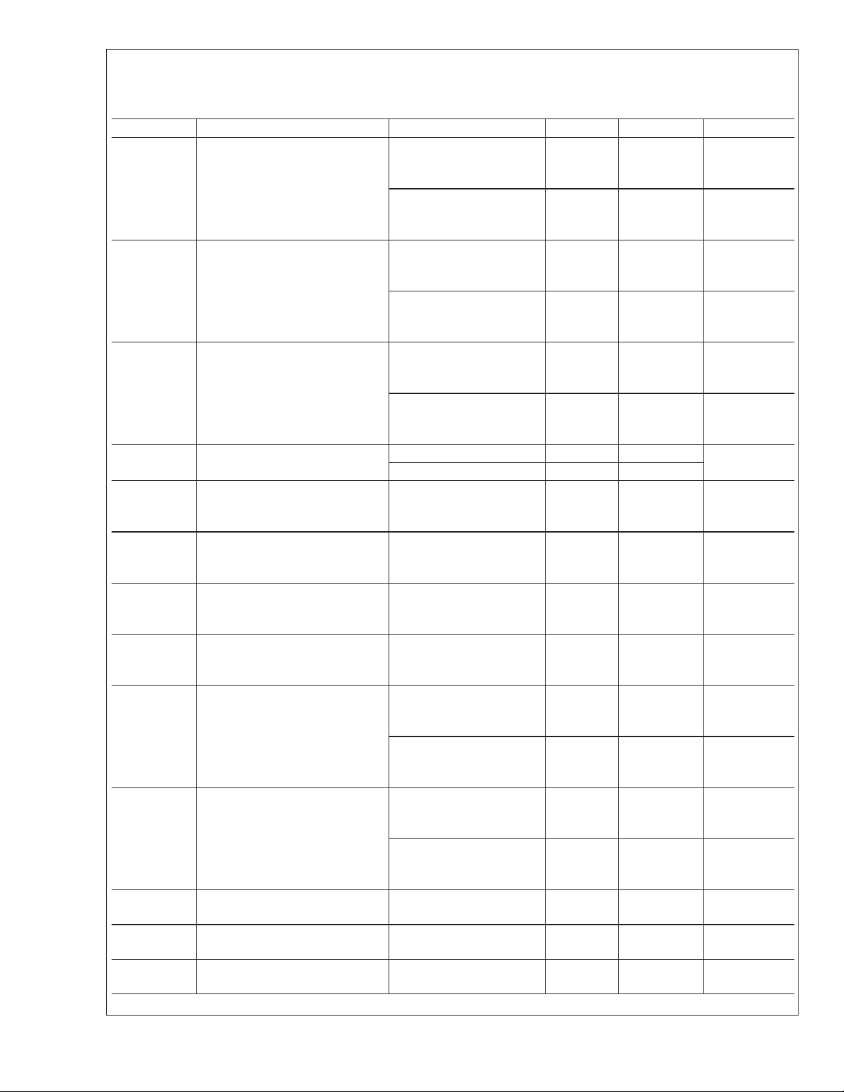
Electrical Characteristics (Note 4) (Continued)
Specifications in Standard type face are for TJ= 25˚C, and in bold type face apply over the full Operating Temperature
Range. Unless otherwise specified, V
Symbol Parameter Conditions Typical Limit Units
V
CL(O)
LM3477/LM3477A
V
CL(100)
Current Limit Voltage at 0% Duty
Cycle
Current Limit Voltage at 100%
Duty Cycle
V
SC
Short-Circuit Current Limit Sense
Voltage
V
SL
Internal Compensation Ramp
Voltage Height
V
OVP
Output Over-voltage Protection
(with respect to feedback
voltage) (Note 7)
V
OVP(HYS)
Output Over-Voltage Protection
Hysteresis(Note 7)
Gm Error Amplifier
Transconductance
A
I
VOL
EAO
Error Amplifier Voltage Gain V
Error Amplifier Output Current
(Source/ Sink)
V
EAO
Error Amplifier Output Voltage
Swing
T
SS
T
r
T
f
Internal Soft-Start Delay VFB= 1.2V, V
Drive Pin Rise Time CGS= 3000pF, VDR=0
Drive Pin Fall Time CGS= 3000pF, VDR=0
IN
= 12V.
LM3477 155
130/125
185/190
LM3477A 165
140/135
195/200
LM3477 74
50/43
98/98
LM3477A 65
41/25
89/98
VIN= 5V, LM3477 350
270
420
= 5V, LM3477A 310
V
IN
260
380
VIN= 5V, LM3477 83 mV
V
= 5V, LM3477A 103
IN
= 1.4V 50
V
COMP
32/25
78/85
V
= 1.4V 60
COMP
20
110
= 1.4V
V
COMP
= 100µA
I
EAO
(Source/Sink)
= 1.4V
COMP
= 100µA
I
EAO
(Source/Sink)
Source, V
V
FB
COMP
=0V
= 1.4V,
750
600/365
1000/1265
38
30
42
100
75/50
130/160
Sink, V
= 1.4V
COMP
= 1.4V, V
FB
−140
−110/−95
−170/−180
Upper Limit
=0V
V
FB
COMP Pin = Floating
Lower Limit
= 1.4V
V
FB
2.2
2.0
2.35
0.75
0.5
0.95
COMP
=
5 msec
Floating
25 ns
to 3V
25 ns
to 3V
mV
mV (min)
mV (max)
mV
mV (min)
mV (max)
mV
mV (min)
mV (max)
mV
mV (min)
mV (max)
mV
mV (min)
mV (max)
mV
mV (min)
mV (max)
mV
mV(min)
mV(max)
mV
mV(min)
mV(max)
µmho
µmho (min)
µmho (max)
V/V
V/V (min)
V/V (max)
µA
µA (min)
µA (max)
µA
µA (min)
µA (max)
V
V(min)
V(max)
V
V(min)
V(max)
www.national.com 4
Page 5
Electrical Characteristics (Note 4) (Continued)
Specifications in Standard type face are for TJ= 25˚C, and in bold type face apply over the full Operating Temperature
Range. Unless otherwise specified, V
Symbol Parameter Conditions Typical Limit Units
V
SD
I
SD
Shutdown Threshold (Note 8) Output = High 1.15
Shutdown Pin Current VSD=5V −1
TSD Thermal Shutdown 165 ˚C
T
SH
θ
JA
Thermal Shutdown Hysteresis 10 ˚C
Thermal Resistance MM Package 200 ˚C/W
IN
= 12V.
Output = Low 0.65
V
=0V +1
SD
1.35
0.3
V (max)
V (min)
µA
LM3477/LM3477A
V
V
www.national.com5
Page 6

Electrical Characteristics (Note 4) (Continued)
Note 1: Absolute Maximum Ratings are limits beyond which damage to the device may occur. Operating Ratings are conditions under which operation of the device
is intended to be functional. For guaranteed specifications and test conditions, see the Electrical Characteristics.
Note 2: The CB pin must not be higher than 8V above the V
Note 3: The human body model is a 100 pF capacitor discharged through a 1.5kΩ resistor into each pin. The machine model is 200 pF capacitor discharged directly
into each pin.
Note 4: All limits are guaranteed at room temperature (standard type face) and at temperature extremes (bold type face). All room temperature limits are 100%
LM3477/LM3477A
tested. All limits at temperature extremes are guaranteed via correlation using standard Statistical Quality Control (SQC) methods. All limits are used to calculate
Average Outgoing Quality Level (AOQL).
Note 5: For this test, the COMP/SD pin must be left floating.
Note 6: For this test, the COMP/SD pin must be pulled low.
Note 7: The over-voltage protection is specified with respect to the feedback voltage. This is because the over-voltage protection tracks the feedback voltage. The
overvoltage protection threshold is given by adding the feedback voltage, V
Note 8: The COMP/SD pin should be pulled to ground to turn the regulator off. The voltage on the COMP/SD pin must be below the limit for Output = Low to keep
the regulator off.
SW
.
to the over-voltage protection specification.
FB
www.national.com 6
Page 7
LM3477/LM3477A
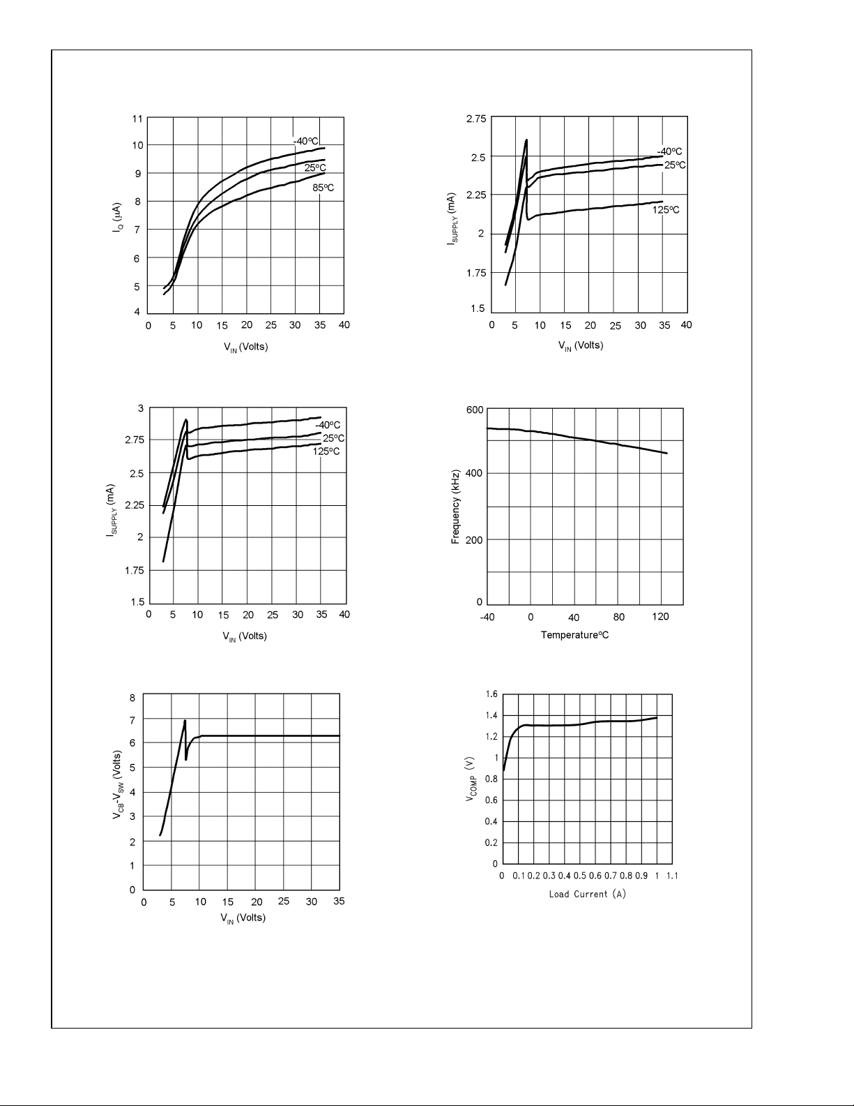
Typical Performance Characteristics Unless otherwise specified, V
(Shutdown) vs Temperature & Supply Voltage I
I
Q
20003313 20003314
I
vs Temperature & Supply Voltage (Switching) Frequency vs Temperature
Supply
vs Temperature & Supply Voltage (Non-Switching)
Supply
= 12V, TJ= 25˚C.
IN
20003315 20003316
VCB−VSWvs Supply Voltage COMP Pin Voltage vs Load Current
20003362
20003320
www.national.com7
Page 8

Typical Performance Characteristics Unless otherwise specified, V
= 12V, TJ= 25˚C. (Continued)
IN
LM3477/LM3477A
Efficiency vs Load Current
(V
= 24V, V
IN
OUT
= 12V)
Efficiency vs Load Current
(V
= 12V, V
IN
= 3.3V) Error Amplifier Gain
OUT
200033J9
Efficiency vs Load Current
(VIN= 5V,
OUT
= 3.3V)
200033K2
200033K1
Error Amplifier Phase Shift COMP Pin Source Current vs Temperature
20003309
www.national.com 8
20003308
20003319
Page 9

LM3477/LM3477A
Typical Performance Characteristics Unless otherwise specified, V
= 12V, TJ= 25˚C. (Continued)
IN
Slope Compensation Ramp vs Slope Compensation
Short Circuit vs Temperature
200033J8
Resistor
Shutdown Threshold Hysteresis vs Temperature Current Sense Voltage vs Duty Cycle
20003312
20003318
200033J7
www.national.com9
Page 10

Functional Block Diagram
LM3477/LM3477A
Functional Description
General Description
The LM3477/A is a switching regulator controller for topologies incorporating a high side switch. The most common of
these topologies is the step-down, or buck, converter. Other
topologies such as the inverting (buck-boost) and inverse
SEPIC (zeta) converters can be realized. This datasheet will
focus on buck converter applications.
The LM3477/A employs current mode control architecture.
Among the many benefits of this architecture are superior
line and load regulation, cycle-by-cycle current limiting, and
simple loop compensation. The LM3477/A features a patented adjustable slope compensation scheme to enable flexible inductor selection. The LM3477/A has a combination of
features that allow its use in a wide variety of applications.
The input voltage can range from 2.97V to 35V, with the
output voltage being positive or negative depending on the
topology. The current limit can be scaled to safely drive a
wide range of loads. An internal soft-start is provided to limit
initial in-rush current. Output over voltage and input under
voltage protection ensure safe operation of the LM3477/A.
Regions of Operation
Pulse width modulation (PWM) is the normal mode of operation. In PWM, the output voltage is well regulated and has a
ripple frequency equal to the switching frequency (500kHz).
20003301
In low load conditions, the part operates in hysteretic mode.
In this mode, the output voltage is regulated between a high
and low value that results in a higher ripple magnitude and
lower ripple frequency than in PWM mode (see OVER VOLT-
AGE PROTECTION section).
200033J2
FIGURE 1. Operating Regions of the LM3477/A
www.national.com 10
Page 11

Functional Description (Continued)
The important differences between the LM3477 and the
LM3477A are summarized in Figure 1. The voltages in Fig-
ure 1 can be referred to the switch current by dividing
through by R
old voltage V
larger load range than the LM3477. Typically, V
for the LM3477, while V
difference in area between the shaded regions give a graphical representation of this. The lightly shaded region is the
extra PWM operating area gained by using the LM3477A.
Thus the benefits of operating in PWM mode such as a well
regulated output voltage with low noise ripple are extended
to a larger load range when the LM3477A is used. While less
significant, the other noteworthy difference between the two
parts is in the short circuit current limit V
is a ceiling limit for the peak sense voltage V
V
SC
the SHORT CIRCUIT CURRENT LIMIT section). V
lower in the LM3477A than in the LM3477 (see the ELEC-
TRICAL CHARACTERISTICS section for limits).
Over Voltage Protection
The LM3477/A has over voltage protection (OVP) for the
output voltage. OVP is sensed at and is in respect to the
feedback pin (pin 3). If at anytime the voltage at the feedback
pin rises to V
CHARACTERISTICS section for limits on V
OVP will cause the drive pin to go low, forcing the power
MOSFET off. With the MOSFET off, the output voltage will
drop. The LM3477/A will begin switching again when the
feedback voltage reaches V
ELECTRICAL CHARACTERISTICS for limits on V
OVP can be triggered by any event that causes the output
voltage to rise out of regulation. There are several common
circumstances in which this can happen, and it is beneficial
for a designer to be aware of these for debugging purposes,
since the mode of operation changes from the normal Pulse
Width Modulation (PWM) mode to the hysteretic mode. In
the hysteretic mode the output voltage is regulated between
a high and low value that results in a higher ripple magnitude
and lower ripple frequency than in the PWM mode, see
Figure 2.
. The LM3477A has a lower hysteretic thresh-
SN
, and thus will operate in PWM mode for a
HYS
FB+VOVP
= 11mV for the LM3477A. The
HYS
.
SC
, OVP is triggered. See ELECTRICAL
+(V
FB
OVP-VOVP(HYS)
FB
HYS
SNpk
and V
OVP(HYS)
= 32mV
(see
SC
OVP
). See
.
LM3477/LM3477A
If the load current becomes too low, the LM3477/A will
increase the duty cycle, causing the voltage to rise and
trigger the OVP. The reasons for this involve the way the
LM3477/A regulates the output voltage, using a control
waveform at the pulse width modulator. This control waveform has upper and lower bounds.
Another way OVP can be tripped is if the input voltage rises
higher than the LM3477/A is able to regulate in pulse width
modulation (PWM) mode. The output voltage is related to
the input voltage by the duty cycle as: V
OUT=VIN
LM3477/A has a minimum duty cycle of 16.5% (typical), due
to the blank-out timing, TMIN. If the input voltage increases
such that the duty cycle wants to be less than D
cycle will hold at D
and the output voltage will increase
MIN
with the input voltage until it trips OVP.
It is useful to plot the operational boundaries in order to
illustrate the point at which the device switches into hyster-
is
etic mode. In Figure 1, the limits shown are with respect to
the peak voltage across the sense resistor R
they can be referred to the peak inductor current by dividing
through by R
SN.VSNpk
normal circumstances V
is bound to the shaded regions. In
is required to be in the shaded
SNpk
region, and the LM3477/A will operate in the PWM mode. If
operating conditions are chosen such that V
normally fall in the shaded regions, then the mode of operation is changed so that V
will be in the shaded region,
SNpk
and the part will operate in the hysteretic mode. What actually happens is that the LM3477/A will not allow V
outside of the shaded regions, so the duty cycle is adjusted.
The output voltage transient response overshoot can also
trigger OVP. As discussed in the OUTPUT CAPACITOR
section, if the capacitance is too low or ESR too high, the
.
output voltage overshoot will rise high enough to trigger
OVP. However, as long as there is room for the duty cycle to
adjust (the converter is not near D
MIN
LM3477/A will return to PWM mode after a few cycles of
hysteretic mode operation.
There is one last way that OVP can be triggered. If the
unregulated input voltage crosses 7.2V, the output voltage
will react as shown in Figure 3. The internal bias of the
LM3477/A switches supplies at 7.2V. When this happens, a
sudden small change in bias voltage is seen by all the
internal blocks of the LM3477/A. The control voltage, VC,
shifts because of the bias change, the PWM comparator
tries to keep regulation. To the PWM comparator, the scenario is identical to step change in the load current, so the
response at the output voltage is the same as would be
observed in a step load change. Hence, the output voltage
overshoot here can also trigger OVP. The LM3477/A will
regulate in hysteretic mode for several cycles, or may not
recover and simply stay in hysteretic mode until the load
current drops. Note that the output voltage is still regulated in
hysteric mode. Predicting whether or not the LM3477/A will
come out of hysteretic mode in this scenario is a difficult
task, however it is largely a function of the output current and
the output capacitance. Triggering hysteretic mode in this
way is only possible at higher load currents. The method to
avoid this is to increase the output capacitance.
MIN
SN
SNpk
or D
*
D. The
, the duty
,(V
SNpk
would not
to be
SNpk
), the
MAX
);
200033C1
FIGURE 2. The Feedback Voltage is related to the
Output Voltage. See different Ripple Components in
PWM and Hysteretic Modes
www.national.com11
Page 12

Functional Description (Continued)
LM3477/LM3477A
FIGURE 3. The Feedback Voltage Experiences an
Oscillation if the Input Voltage Crosses the 7.2V
Internal Bias Threshold
Default/Adjustable Slope Compensation
The LM3477/A uses a current mode control scheme. There
are many advantages in a current mode architecture including inherent cycle-by-cycle current limiting and simple compensation of the control loop. However, there are consequences to using current mode control that one must be
aware of while selecting circuit components. One of these
consequences is the inherent possibility of subharmonic oscillations in the inductor current. This is a form of instability
and should be avoided.
200033J6
switching cycles. The two solid waveforms shown are the
waveforms compared at the internal pulse width modulator,
used to generate the MOSFET drive signal. The top waveform with the slope S
waveform V
. The bottom waveform with slopes Snand Sfis
C
the sensed inductor current waveform V
is the internally generated control
e
. These signals
SEN
are compared at the PWM comparator. There is a feedback
loop involved here. The inductor current is sensed and fed
back to the PWM comparator, where it is compared to V
The output of the comparator in combination with the R/S
latch determine if the MOSFET is on or off, which effectively
controls the amount of current the inductor receives. While
is higher than V
V
C
, the PWM comparator outputs a high
SEN
signal, driving the external power MOSFET on. When MOSFET is on, the inductor current rises at a constant slope,
generating the sensed voltage V
SEN
. When V
equals VC,
SEN
the PWM comparator signals to drive the MOSFET off, and
the sensed inductor current decreases with a slope S
process begins again when R
latch is set by an internal
S
. The
f
oscillator.
The subharmonic oscillation phenomenon is realized when a
load excursion is experienced. The way it is analyzed is to
calculate how the inductor current settles after such an
excursion. Take for example the case when the inductor
current experiences a step increase in its average current,
shown as the dotted line in Figure 4. In the switching period
that the excursion occurs, the inductor current will change by
. In the following switching period, the inductor current will
∆I
0
have a difference ∆I
from its original starting value. The
1
original excursion is being propagated each switching cycle.
What is desired is to find out if this propagation is converging
or diverging. It is apparent that the difference in the inductor
current from one cycle to the next is a function of S
, as follows:
S
e
n,Sf
, and
.
C
200033C2
FIGURE 4. The Current Sensing Loop and
Corresponding Waveforms
As a brief explanation, consider Figure 4. A lot of information
is shown here. The top portion shows a schematic of the
current sensing loop. The bottom portion shows the pulse
width modulation (PWM) comparator waveforms for two
Hence, if the quantity (Sf-Se)/(Sn+Se)is greater than 1, the
inductor current diverges and subharmonic oscillations result. Notice that as S
increases, the factor decreases. Also,
e
when the duty cycle is greater than 50%, as the inductance
become less, the factor increases.
The LM3477/A internally generates enough slope compensation S
height of the compensation slope ramp V
to allow for the use of reasonable inductances. The
e
can be found in
SL
the ELECTRICAL CHARACTERISTICS section. The
LM3477/A incorporates a patented scheme to increase S
e
there is need to use a smaller inductor. With the use of a
single resistor R
, Se can be increased indefinitely. R
SL
increases the compensation slope Se by the amount:
Therefore,
When excursions of the inductor current are divergent, the
current sensing control loop is unstable and produces a
subharmonic oscillation in the inductor current. This oscillation is viewed as a resonance in the outer voltage control
loop at half the switching frequency. In the inductor section,
if
SL
www.national.com 12
Page 13

Functional Description (Continued)
calculations for minimum inductance and necessary slope
resistance R
ing.
Start-up/Soft-start
The LM3477/A incorporates an internal soft-start during
start-up. The soft-start forces the inductor current to rise
slowly and smoothly as it increases towards the steady-state
current. This technique is used to reduce the input inrush
current during soft-start. The soft-start functionality is effective for approximately the first 5ms of start-up.
Note: The LM3477/A will not start-up if the output voltage is being held up
externally by more than 200mV.
If the slope resistor R
of pre load to successfully start up.
Short Circuit Protection
When the voltage across the sense resistor (measured as
the V
IN−ISEN
current limit gets activated. In the short-circuit protection
mode, the external MOSFET is turned off. When the short is
removed, the external MOSFET is turned on after five
cycles. The short circuit protection voltage V
the ELECTRICAL CHARACTERISTICS section. V
lower in the LM3477A than in the LM3477.
are carried out based on this resonant peak-
SL
is used, the LM3477/Amay need up to 100 mA
SL
differential voltage) exceeds VSC, short-circuit
is specified in
SC
SC
LM3477/LM3477A
Design Section
General
Power supply design involves making tradeoffs. To achieve
performance specifications, limitations will be set on component selection. The LM3477/A provides many degrees of
flexibility in choosing external components to accommodate
various performance/component selection optimizations. For
example, the internal slope compensation can be externally
increased to allow smaller inductances to be used. The
design procedures that follow provide instruction on how to
select the external components in a typical LM3477/A buck
circuit in continuous conduction mode, as well as aid in the
optimization of performance and/or component selection.
See Figure 6 for component reference and typical circuit.
The LM3477/A may also be designed to operate in discontinuous conduction mode.
is
Shutdown
The compensation pin (Pin 2) of LM3477/A also functions as
a shutdown pin. If a low signal (refer to the ELECTRICAL
CHARACTERISTICS for definition of low signal) appears on
the COMP/SD pin, the LM3477/A stops switching and goes
into a low supply current mode. The total supply current of
the IC reduces to less than 10µA under these conditions.
Figure 5 shows different implementations of the shutdown
function.
20003325
200033M8
FIGURE 6. LM3477 Buck Converter Reference
Schematic
Programming the Output Voltage
The output voltage can be programmed using a resistor
divider between the output and the feedback pins, as shown
in Figure 6. The resistors are selected such that the voltage
at the feedback pin is 1.27V. R
FB1
and R
can be selected
FB2
using the equation:
V
OUT
= 1.27*(1+ R
FB1/RFB2
)
Calculating the Duty Cycle
In buck converter applications, the duty cycle of the
LM3477/A may be calculated as:
FIGURE 5. Implementing Shutdown in LM3477
20003326
Where
= forward drop of the power diode ) 0.5V
V
D
=VDSof the MOSFET when it is conducting )
V
Q
*
R
I
OUT
DSON
VSN= Voltage across the sense resistor = I
OUTxRSN
www.national.com13
Page 14

Design Section (Continued)
This is the fraction of the switching period that the switch is
on. The switch is off for the remainder of the period. This
fraction is expressed as:
D’=1−D
The LM3477/A has limits for the maximum and minimum
LM3477/LM3477A
duty cycle (see ELECTRICAL CHARACHTERISTICS). The
maximum duty cycle of 93% (typical) will limit how low the
input voltage may drop while maintaining a regulated output
voltage (the dropout voltage). In situations where a very low
dropout voltage is required, it is necessary to include V
and VSNlosses in the maximum duty cycle calculation.
Voltage drops in the inductor will lower the dropout voltage
as well.
The minimum duty cycle of the LM3477/A corresponds to the
minimum on time, or blank out time (see ELECTRICAL
CHARACHTERISTICS).
*
D
MIN=TMIN
This will not limit how high the input voltage can rise, however the LM3477/A will operate in hysteretic mode once the
operating duty cycle decreases to the minimum duty cycle.
f
s
D,VQ
Programming the Current Limit/Hysteretic Threshold
DEFINITIONS:
Current Limit: The current limit is the point at which the
LM3477/A begins to limit the peak switch current. The current limit in the LM3477/A varies with duty cycle, which is a
function of the V
IN−VOUT
differential.
Hysteric Threshold: Hysteretic threshold is the current at
which the LM3477/A enters the hysteretic mode of operation
(see OVER VOLTAGE PROTECTION section). The hyster-
etic threshold is with respect to the peak switch current.
Setting Current Limit and Hysteretic Threshold
The adjustable current limit of the LM3477/A is set by the
sense resistor R
an internal control voltage V
when V
SEN(peak)
here as the differential voltage from the V
. The voltage across RSNis compared to
SN
equals V
. The onset of current limiting is
C
C(max)
,orVCL.V
SEN
pin to the I
IN
is defined
SEN
pin. VCLdecreases as the duty cycle increases, as shown in
Figure 7. Therefore, it is important to know both V
and V
V
IN
condition.
at the maximum operating duty cycle, or lowest
CL(min)
SEN(peak)
200033K3
FIGURE 7. Current Limit and Hysteretic Threshold vs
Duty Cycle
V
where D
CL(MIN)
=V
CL(0)(MIN)
is the duty cycle at the lowest VINcondition.
MAX
−D
(MAX)(VCL(0)(MIN)
−V
CL(100)(MIN)
To avoid current limit,
V
SEN(peak)
<
V
CL(MIN)
Therefore,
)
www.national.com 14
Page 15

Design Section (Continued)
LM3477/LM3477A
Example: V
IN(MIN)
= 4.5V, V
OUT
= 2.5V, I
OUT(MAX)
=3A
The hysteretic threshold is derived in a similar manner, the
only difference being that V
(V
). Notice that V
HYS
does not vary with the duty cycle.
HYS
SEN(peak)
is compared V
C(min)
The hysteretic threshold is predetermined by the selection of
above. The hysteretic threshold is:
R
SN
Continuing with the example above,
If the peak switch current decreases below this threshold,
the LM3477/A will operate in hysteretic mode (see OVER
VOLTAGE PROTECTION section). In some designs, it will
be desired to use R
so that lower valued inductors can be
SL
used (see DEFAULT/ADJUSTABLE SLOPE COMPENSA-
TION section and Inductor section). Using R
current limit and the hysteretic threshold. See Figure 8.R
will lower the
SL
SL
effectively adds an additional slope to the existing slope of
waveform.
the V
C
200033K4
FIGURE 8. Current Limit and Hysteretic Threshold vs
When R
Duty Cycle with R
is used, the following equations apply:
SL
SL
where MIN(V
the two values in the parenthesis and V
0.011V for the LM3477 and LM3477A, respectively. R
− 50x10-6xRSLxD
HYS
, 0) is the smaller of
MAX
is 0.032V and
HYS
can
SL
be used creatively to intentionally lower the hysteretic
threshold, allowing for better performance at lower loads.
However, when R
is used, there may be a minimum load
SL
requirement (see START-UP/SOFT-START section).
Power Inductor Section
The LM3477/A operates at a high switching frequency of
500kHz, which allows the use of small inductors. This is
made apparent in the following set of equations used to
calculate the output voltage ripple.
∆V
OUT(Pk-Pk)
) ∆i
L(Pk-Pk)
xR
ESR
(V)
As the switching frequency fs increases, the inductance
required for a given output voltage ripple decreases. The
equations above for ∆V
and ∆iLprovide criteria for
OUT
choosing the inductance. The maximum voltage ripple in
steady-state, PWM operation can be controlled by limiting
which in turn is set by the inductance value. Alternatively,
∆i
L
one can simply choose ∆i
as a percentage of the maximum
L
output current. Clearly, the size of the output capacitor ESR,
, will have an affect on which criteria is used to choose
R
ESR
the inductance. When the ESR is relatively low (less than
100mΩ), such as in ceramic, OSCON, and some low ESR
tantalum capacitors, it is convenient to choose the inductance based on setting ∆i
high, then it may be necessary to restrict ∆i
to 30% of Iout(max). If the ESR is
L
to a lower value
L
so that the output voltage ripple is not too high. Generally
speaking, the former suggestion of setting ∆i
I
OUT(MAX)
is recommended.
to 30% of
L
The inductance also affects the stability of the converter. The
slopes S
while the compensation ramp, S
and Sfin Figure 4 are functions of the inductance,
n
, is fixed by default. There-
e
fore if the inductance is too small, the converter may experience sub-harmonic oscillations. The LM3477/A provides
sufficient internal slope compensation to allow for inductances chosen according to the ∆i
=0.3xI
L
guideline in
OUT
most cases. Still, one should check to make sure the inductance is not too low before continuing the design process. If
it is found that the selected inductance is too low, a patented
scheme to increase the compensation ramp, S
, is provided
e
in the LM3477/A (see DEFAULT/ADJUSTABLE SLOPE
COMPENSATION section). In the calculations that follow, if it
is found that the chosen inductance is too small, R
SL
can be
used to increase Se so that the inductance can be used.
In a current mode control architecture, there is an inherent
resonance at half the switching frequency (see
DEFAULT/ADJUSTABLE SLOPE COMPENSATION sec-
www.national.com15
Page 16

Design Section (Continued)
tion). A convenient indicator of how much resonance exists is
quality factor Q. If Q is too high, subharmonic oscillations
could occur, if Q is too low, the current mode architecture
begins to act like a voltage mode architecture and the necessary compensation becomes more complex. This is dis-
LM3477/LM3477A
cussed in more detail in the COMPENSATION section, but
here it is important to calculate Q to be sure the selected
inductance will not cause problems to the stability of the
converter. The calculations below call for an inductance that
results in Q between 0.15 and 2. See the COMPENSATION
section if the chosen inductance enforces Q to be out of this
range. By default, no extra slope compensation is needed,
= 0. In general, a Q between 0.5 and 1 is optimal.
so R
SL
Where,
D’ = 1−D
VQ=VDSof the MOSFET when it is conducting
*
R
I
OUT
DS(ON).
V
= Voltage across the sense resistor ) I
SEN
Back solving for L gives a range for acceptable inductances
based on a range for Q:
OUTxRSN
Type of output capacitors
Different type of capacitors often have different combinations
of capacitance, equivalent series resistance (ESR), and voltage ratings. High-capacitance multi-layer ceramic capacitors
(MLCCs) have a very low ESR, typically 12mΩ, but also
relatively low capacitance and low voltage ratings. Tantalum
capacitors can have fairly low ESR, such as 18mΩ, and high
capacitance (up to 1mF) at higher voltage ratings than MLCCs. Aluminum capacitors offer high capacitance and relatively low ESR and are available in high voltage ratings.
OSCON capacitors can achieve ESR values that are even
lower than those of MLCCs and with higher capacitance, but
the voltage ratings are low. Other tradeoffs in capacitor
technology include temperature stability, surge current capability, and capacitance density (physical size vs. capacitance).
Output Capacitor Considerations
Skip to the ’Calculations for the output capacitor’ subsection
if a quick design is desired. While it is generally desired to
use as little output capacitance as possible to keep costs
down, the output capacitor should be chosen with care as it
directly affects the ripple component of the output voltage as
well as other components in the design. The output voltage
ripple is directly proportional to the ESR of the output capacitor (see POWER INDUCTOR section). Therefore, designs
requiring low output voltage ripple should have an output
capacitor with low ESR. Choosing a capacitor with low ESR
has the additional benefit of requiring one less component in
the compensation network, as discussed in the Compensation section.
In addition to the output voltage ripple, the output capacitor
directly affects the output voltage overshoot in a load transient. Two transients are possible: an unloading transient
and a loading transient. An unloading transient occurs when
the load current transitions to a higher current, and charge is
unloaded from the output capacitor. A loading transient is
when the load transitions to a lower current, and charge is
loaded to the output capacitor. How the output voltage reacts
during these transitions is known as the transient response.
Both the capacitance and the ESR of the output capacitor
will affect the transient response.
It is recommended that:
Q(max) = 2, and
Q(min) = 0.15
Values for V
can be found in the ELECTRICAL CHARAC-
SL
TERISTICS section.
Note: Adding slope compensation with R
will decrease the
SL
current limit. An iterative process may be needed to meet
current limit and stability requirements, see PROGRAM-
MING CURRENT LIMIT/HYSTERETIC THRESHOLD section.
Output Capacitor Selection
A capacitance between 47µF - 100µF is typically used. Skip
to ’Calculations for the Output Capacitance’ for minimum
capacitance calculations.
www.national.com 16
200033B9
FIGURE 9. A Loading Transient
The control loop of the LM3477/A can be made fast enough
to saturate the duty cycle when the worst case lode transient
occurs. This means the duty cycle jumps to D
MIN
or D
MAX
depending on the type of load transient. In a loading transient, as shown in Figure 9, the duty cycle drops to D
MIN
while the inductor current falls to match the load current.
During this time, the regulator is heavily dependent on the
output capacitors to handle the load transient. The initial
overshoot is caused by the ESR of the output capacitors.
,
Page 17

Output Capacitor Selection
(Continued)
How the output voltage recovers after that initial excursion
depends on how fast the inductor current falls and how large
the output capacitance is. See Figure 10.
200033B5
FIGURE 10. Output Voltage Overshoot Violation
The ESR and the capacitance of the output capacitor must
be carefully chosen so that the output voltage overshoot is
within the design’s specification V
bined ESR of the output capacitors is not low enough, the
initial output voltage excursion will violate the specification,
see ∆V
. If the ESR is low enough, but there is not enough
C1
output capacitance, the output voltage will travel outside the
specification window due to the extra charge being dumped
into the capacitor, see ∆V
. The LM3477/A has output over
C2
voltage protection (OVP) which could trigger if the transient
overshoot is high enough. If this happens, the controller will
operate in hysteretic mode (see OVER VOLTAGE PROTEC-
TION section) for a few cycles before the output voltage
settles to its steady state. If this behavior is not desired,
substitute V
(referred to the output) for V
OVP
found in the ELECTRICAL CHARACTERISTICS table) to
find the minimum capacitance and maximum ESR of the
output capacitor.
Calculations for the Output Capacitor
During a loading transient, the delta output voltage ∆V
two changing components. One is the voltage difference
across the ESR (∆V
caused by the gained charge (∆V
), the other is the voltage difference
r
q
= ∆Vr+ ∆V
∆V
c
The design objective is to keep ∆Vclower than some maximum overshoot (V
OS(MAX)
). V
OS(MAX)
the output load requirements.
Both voltages ∆V
and ∆Vqwill change with time. For ∆Vrthe
r
equation is:
where,
= the output capacitor ESR
R
ESR
∆I
= the difference between the load current change
OUT
I
OUT(MAX)−IOUT(MIN)
D
= Minimum duty cycle of device (0.165 typical)
MIN
Evaluating this equation at t = 0 gives ∆V
V
OS(MAX)
for ∆V
and solving for R
r(MAX)
. If the total com-
OS(MAX)
OS(MAX)(VOVP
). This gives:
q
is chosen based on
. Substituting
r(max)
gives:
ESR
has
c
LM3477/LM3477A
The expression for ∆Vqis:
From Figure 11 it can be told that ∆VCwill reach its peak
value at some point in time and then decrease. The larger
the output capacitance is, the earlier the peak will occur. To
find the peak position, let the derivative of ∆V
go to zero,
C
and the result is:
200033B6
FIGURE 11. Output Voltage Overshoot Peak
is
The intention is to find the capacitance value that will yield, at
,a∆VCthat equals V
t
peak
equating ∆V
C
OUT(MIN)
C
:
to V
OS(max)
. Substituting tpeak for t and
OS(max)
gives the following solution for
The chosen output capacitance should not be less than
47µF, even if the solution for C
OUT(MIN)
is less than 47µF.
Notice it is already assumed that the total ESR is no greater
than R
ESR(MAX)
, otherwise the term under the square root
will be a negative number.
Power MOSFET Selection
The drive pin of LM3477/A must be connected to the gate of
an external MOSFET. In a buck topology, the drain of the
external N-Channel MOSFET is connected to the input and
the source is connected to the inductor. The C
provides the gate drive needed for an external N-Channel
MOSFET. The gate drive voltage depends on the input voltage (see TYPICAL PERFORMANCE CHARACTERISTICS).
In most applications, a logic level MOSFET can be used. For
very low input voltages, a sub-logic level MOSFET should be
used.
The selected MOSFET directly controls the efficiency. The
critical parameters for selection of a MOSFET are:
1. Minimum threshold voltage, V
2. On-resistance, R
DS
(ON)
TH
(MIN)
pin voltage
B
www.national.com17
Page 18

Power MOSFET Selection (Continued)
3. Total gate charge, Q
4. Reverse transfer capacitance, C
5. Maximum drain to source voltage, V
The off-state voltage of the MOSFET is approximately equal
LM3477/LM3477A
to the input voltage. V
greater than the input voltage. The power losses in the
MOSFET can be categorized into conduction losses and ac
switching or transition losses. R
the conduction losses. The conduction loss, P
2
R loss across the MOSFET. The maximum conduction loss
I
is given by:
where D
is the maximum operating duty cycle:
MAX
The turn-on and turn-off transition times of a MOSFET from
the MOSFET specifications require tens of nano-seconds.
and Qgare needed from the MOSFET specifications to
C
RSS
estimate the large instantaneous power loss that occurs
during these transitions.
The average amount of gate current required to turn the
MOSFET on can be calculated using the formula:
The required gate drive power to turn the MOSFET on is
equal to the switching frequency times the energy required
to deliver the charge to bring the gate charge voltage to V
(see ELECTRICAL CHARACTERISTICS and TYPICAL
PERFORMANCE CHARACTERISTICS for the drive voltage
specification).
It is sometimes helpful or necessary to slow down the turn on
transition of the FET so that less switching noise appears at
the I
R
pin. This can be done by inserting a drive resistor
SEN
in series with the boot-strap capacitor (see Figure 6).
DR
This can help reduce sensing noise that may be preventing
designs from operating at or near the LM3477/A’s minimum
duty cycle limit. Gate drive resistors from 2.2Ω to 51Ω are
recommended.
g
DS(MAX)
I
P
Drive=FS.Qg.VDR
of the MOSFET must be
DS(ON)
G=Qg.FS
RSS
DS(MAX)
is needed to estimate
Power Diode Selection
The output current commutates through the diode when the
external MOSFET turns off. The three most important parameters for the diode are the peak current, peak inverse
voltage, and average power dissipation. Exceeding these
ratings can cause damage to the diode. The average current
through the diode is given by:
I
D(AVG)=IOUT
where D is the duty cycle and I
diode must be rated to handle this current.
The off-state voltage across the diode in a buck converter is
approximately equal to the input voltage. The peak inverse
voltage rating of the diode must be greater than the off-state
voltage of the diode. To improve efficiency, a low forward
drop schottky diode is recommended.
x (1-D)
is the output current. The
OUT
COND
,isthe
DR
Input Capacitor Selection
In a buck converter, the high side switch draws large ripple
currents from the input capacitor. The input capacitor must
be rated to handle this RMS current.
The power dissipated in the input capacitor is given by:
P
D(CIN)=IRMS_CIN
where R
ESR_CIN
2
R
ESR_CIN
,
is the ESR of the input capacitor. The input
capacitor must be selected to handle the rms current and
must be able to dissipate the power. P
D(CIN)
must be lower
than the rated power dissipation of the selected input capacitor. In many cases, several capacitors have to be paralleled
to handle the rms current. In that case, the power dissipated
in each capacitor is given by:
P
D(CIN)
=(I
RMS_CIN
R
ESR_CIN
)/n2, where n is the total num-
2
ber of capacitors paralled at the input.
A 0.1µF or 1µF ceramic bypass capacitor is also recom-
mended on the V
pin (pin 8) of the IC. This capacitor must
IN
be connected very close to pin 8.
Compensation
20003391
FIGURE 12. Control Block Diagram of a Current Mode
Controlled Buck Converter
The LM3477/A is a current mode controller, therefore the
control block diagram representation involves 2 feedback
loops (see Figure 12). The inner feedback loop derives its
feedback from the sensed inductor current, while the outer
loop monitors the output voltage. This section will not give a
rigorous analysis of current mode control, but rather a simplified but accurate method to determine the compensation
network. The first part reveals the results of the model, giving
expressions for solving for component values in the compensation network.
The compensation network is designed around the power
components, or the power stage. An isolated schematic of
the error amplifier and the various compensation components is shown in Figure 13. The error amplifier in conjunction with the compensation network makes up the compensator block in Figure 12. The purpose of the compensator
block is to stabilize the control loop and achieve high performance in terms of the transient response, audio susceptibility and output impedance.
www.national.com 18
Page 19

Compensation (Continued)
There are several different types of compensation that can
be used to improve the frequency response of the control
loop. To determine which compensation scheme to use,
some information about the power stage is needed.
Use V
IN=VIN(MIN)
and R = R
MIN(IOUT(MAX)
) when calculat-
ing compensation components.
LM3477/LM3477A
20003390
FIGURE 13. LM3477 Compensation Components
Figure 14 shows a bode plot of a typical current mode buck
regulator. It is an estimate of the actual plot using the asymptotic approach. The three plots shown are of the compensator, powerstage, and loop gain, which is the product of
the power stage, compensator, and feedback gain. The loop
gain determines both static and dynamic performance of the
converter. The power stage response is fixed by the selection of the power components, therefore the compensator is
designed around the powerstage response to achieve a
good loop response. Specifically, the compensator is added
to increase low frequency magnitude, extend the 0dB frequency (crossover frequency), and improve the phase characteristic.
200033J4
FIGURE 14. Typical Open Loop, Compensator, and
Power Stage Bode Plots for LM3477 Buck Circuits.
Poles, Zeros and Important Measurements are Labeled
Se=fS(VSL+ 50x10−6RSL)
With the power stage known, a compensator can be designed to achieve improved performance and stability. The
LM3477/A will typically require only a single resistor and
capacitor for compensation, but depending on the power
stage it could require three or four external components.
It is a good idea to check that Q is between 0.15 and 2, if it
was not already done when selecting the inductor. If Q is less
than 0.15 or greater than 2, skip to the SAMPLING POLE
QUALITY FACTOR section below before continuing with the
compensator design.
First, a target crossover frequency (f
) for the loop gain must
c
be selected. The crossover frequency is the bandwidth of the
converter. A higher bandwidth generally corresponds to
faster response times and lower overshoots to load transients. However, the bandwidth should not be much higher
than 1/10 the switching frequency. The LM3477/A operates
with a 500kHz switching frequency, so it is recommended to
choose a crossover frequency between 10kHz - 50kHz.
The schematic of the LM3477/A compensator is shown in
Figure 13. The default design uses R
(type 2) compensator. The C
C2
and CC1to form a lag
c
capacitor can be added to
form an additional pole that is typically used to cancel out the
esr zero of the output capacitor. Finally, if extra phase margin
is needed, the Cff capacitor can be added (this does not help
at low output voltages, see below).
www.national.com19
Page 20

Compensation (Continued)
The strategy taken here for choosing R
crossover frequency with R
with C
set R
. Using the selected target crossover frequency, fC,
C1
to:
C
, and set the compensator zero
c
and CC1is to set the
c
LM3477/LM3477A
fC= Crossover frequency in Hertz (20kHz - 50kHz is recommended)
= 50x103Ω
R
GM
GM = 1000x10
The compensator zero, f
sient responses are desired, f
possible, however it should not be higher than the selected
crossover frequency f
choose C
power pole f
frequency fc:
In this compensation scheme, the pole created by CC2is
used to cancel out the zero created by the ESR of the output
capacitor. In other schemes such as the methods discussed
in the SAMPLING POLE QUALITY FACTOR subsection, the
ESR zero is used. For the typical case, use C
−6
A/V
, is set with CC1. When fast tran-
Z1
should be placed as high as
Z1
. The guideline proposed here is to
such that fZ1falls somewhere between the
C1
P1
C
and1⁄2decade before the selected crossover
One can plot the magnitude and phase of the open loop
response to analyze the frequency response.
Example: Compensation Design
4.5V ≤ V
V
OUT
I
OUT
R
SN
≤ 5.5V
IN
= 2.5V
= 3A (R = 0.83Ω)
= 0.02Ω
L = 3.3µH
=0Ω
R
SL
= 100µF
C
OUT
= 0.01Ω
R
ESR
First, calculate the power stage parameters using V
and R
if:
C2
(MAX)
:
IN(MIN)
Plotting the Open Loop Response
The open loop response is expressed as:
T=ADCxACMxHxFp(s)xFc(s)
Where A
A
CM
www.national.com 20
and H are given above and
DC
=GMxR
GM
In this example, a crossover frequency of 20kHz is chosen,
= 20000. RCis now calculated using the power stage
so: f
C
information and the target crossover frequency f
:
C
This sets the high frequency gain of the compensator such
that a crossover frequency of f
sets the compensator zero, fZ2. Set fZ2between the
C
C1
power pole f
over frequency f
and the1⁄2decade before the target cross-
P1
:
C
is obtained. The capacitor
C
Page 21

Compensation (Continued)
Choosing C
the power pole and insuring a −20dB/decade slope in the
low frequency magnitude response. In other words, the
phase margin below the crossover frequency will always be
higher than the phase margin at the crossover frequency.
If better transient response times are desired, a second
method is to set f
target crossover frequency. This trades more low frequency
gain for less phase margin, which translates to faster but
more oscillatory step responses. We pick C
47nF).
If the esr zero of the output capacitor (f
more phase margin is required, additional components may
be added to increase the flexibility of the compensator.
Use C
C2
= 88x10−9F will set fZ2=fP1, canceling out
C1
between fP1and1⁄2decade before fC, the
Z2
C1
) is too low or if
ESR
1
<
if f
ESR
⁄2fS, that is if:
= 49nF (use
stage equations above, Q, describes how much resonance
will be observed. Q is a function of duty cycle and m
. Figure
c
16 shows how the power stage bode plot is affected as Q is
varied from 0.01 to 10. The resonance is caused by two
complex poles at half the switching frequency. If m
is too
c
low, the resonant peaking could become severe coinciding
with subharmonic oscillations in the inductor current. If m
c
too high, the two complex poles split and the converter
begins to act like a voltage mode converter and the compensation scheme used above should be changed.
LM3477/LM3477A
is
For this example, f
= 159 kHz, so use CC2.
ESR
The equations used here for RC,CC1, and CC2are approxi-
<<
mations valid when C
CC1. For exact equations, see
C2
Plotting Open Loop Response earlier in this section. In some
cases, the desired inductance is several times higher than
the optimal inductance set by the internal slope compensation. This results in a Q lower than 0.15, in which case
additional methods of compensating are presented (see
SAMPLING POLE QUALITY FACTOR section).
200033J3
FIGURE 15. Open Loop Frequency Response for
LM3477 Compensation Design Example
200033J5
FIGURE 16. The Quality Factor Q of the Two Complex
Poles is used to qualify how much resonant peaking is
observed in the Power Stage Bode Plot
>
2, the sampling poles are imaginary and are approach-
If Q
ing the right half of the imaginary plane (the system is
becoming unstable). In this case, Q must be decreased by
either increasing the inductance, or more preferably, adding
more slope compensation through the R
resistor (see
SL
DEFAULT/ADJUSTABLE SLOPE COMPENSATION section).
<
0.15, it means that one of the sampling poles is de-
If Q
creasing in frequency towards the dominant power pole, f
p1
There are three ways to compensate for this. Decrease the
crossover frequency, add a phase lead network, or use the
output capacitor’s ESR to cancel out the low frequency
sampling pole.
One option is to decrease the crossover frequency so that
the phase margin is not as severely decreased by the sampling pole. Decreasing the crossover frequency to between
1kHz to 10kHz is advisable here. As a result, there will be a
decrease in transient response performance.
Another option is the use of the feed-forward capacitor, Cff.
This will provide a positive phase shift (lead) which can be
used to increase phase margin. However, it is important to
note that the effectiveness of Cff decreases with output
voltage. This is due to the fact that the frequencies of the
zero f
and pole f
zff
get closer together as the output voltage
pff
is reduced.
The frequency of the feed-forward zero and pole are:
.
Sampling Pole Quality Factor
In a current mode control architecture, there is an inherent
resonace at half the switching frequency. The LM3477/A
internally compensates for this by adding a negative slope to
the PWM control waveform (see DEFAULT/ADJUSTABLE
SLOPE COMPENSATION section). The factor in the power
www.national.com21
Page 22

Compensation (Continued)
LM3477/LM3477A
A third option is to strategically place the ESR zero f
ESR
the output capacitor to cancel out the sampling pole. In this
case, the capacitor C
should be placed around the crossover frequency fc, but
f
ESR
will not be used to cancel out f
C2
ESR
this will depend on how low Q is.
of
.
www.national.com 22
Page 23

Physical Dimensions inches (millimeters)
unless otherwise noted
LM3477/LM3477A High Efficiency High-Side N-Channel Controller for Switching Regulator
8 Lead Mini SO-8 Package
NS Package Number MUA08A
LIFE SUPPORT POLICY
NATIONAL’S PRODUCTS ARE NOT AUTHORIZED FOR USE AS CRITICAL COMPONENTS IN LIFE SUPPORT
DEVICES OR SYSTEMS WITHOUT THE EXPRESS WRITTEN APPROVAL OF THE PRESIDENT AND GENERAL
COUNSEL OF NATIONAL SEMICONDUCTOR CORPORATION. As used herein:
1. Life support devices or systems are devices or
systems which, (a) are intended for surgical implant
into the body, or (b) support or sustain life, and
whose failure to perform when properly used in
accordance with instructions for use provided in the
2. A critical component is any component of a life
support device or system whose failure to perform
can be reasonably expected to cause the failure of
the life support device or system, or to affect its
safety or effectiveness.
labeling, can be reasonably expected to result in a
significant injury to the user.
National Semiconductor
Corporation
Americas
Email: support@nsc.com
www.national.com
National Semiconductor
Europe
Fax: +49 (0) 180-530 85 86
Email: europe.support@nsc.com
Deutsch Tel: +49 (0) 69 9508 6208
English Tel: +44 (0) 870 24 0 2171
Français Tel: +33 (0) 1 41 91 8790
National Semiconductor
Asia Pacific Customer
Response Group
Tel: 65-2544466
Fax: 65-2504466
Email: ap.support@nsc.com
National Semiconductor
Japan Ltd.
Tel: 81-3-5639-7560
Fax: 81-3-5639-7507
National does not assume any responsibility for use of any circuitry described, no circuit patent licenses are implied and National reserves the right at any time without notice to change said circuitry and specifications.
 Loading...