

Page 1
May 1999
LM3460-1.2, -1.5
Precision Controller for GTLp and GTL Bus Termination
LM3460-1.2, -1.5 Precision Controller for GTLp and GTL Bus Termination
General Description
The LM3460 is a monolithic integrated circuit designed for
precision control of GTLplus and GTL Bus termination. This
controller is available in a tiny SOT23-5 package, and includes an internally compensated op amp, a bandgap reference, an NPN output transistor,andvoltage setting resistors.
A trimmed precision bandgap voltage reference utilizes temperature drift curvature correction for excellent voltage stability over the operating range. The precision output control enables the termination voltage to maintain tight regulation,
despite fast switching requirements on the bus.
The LM3460 controller is designed to be used with a high
>
current (
rent needed for the bus termination. The wide bandwidth of
the feedback loop provides excellent transient response,
and greatly reduces the output capacitance required, thus
reducing cost and board space requirements.
7A) NPN pass transistor to provide the high cur-
Features
n Precision output (1%)
n Output voltage can be adjusted
n Extremely fast transient response in GTLp and GTL bus
termination
n Tiny SOT23-5 package
n Output voltage capability for GTL or GTLp
n Low temperature coefficient
Applications
n GTL bus termination (1.2V output 7A)
n GTLp bus termination (1.5V output 7A)
n Adjustable high-current linear regulator
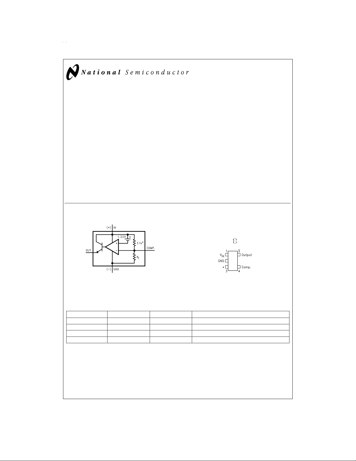
Connection Diagram and Package Information
*
This resistor is not used on the LM3460-1.2.
LM3460 Functional Diagram
DS012603-1
*
No internal connection, but should be soldered to PC board for best heat
transfer.
5-Lead Outline Package (M5)
Actual Size
DS012603-2
DS012603-3
Top View
See NS package Number MA05B
Ordering Information
Voltage Order Number Package Marking Supplied As
1.5 LM3460M5-1.5 D06A 250 Unit Increments on Tape and Reel
1.5 LM3460M5X-1.5 D06A 3k Unit Increments on Tape and Reel
1.2 LM3460M5-1.2 D09A 250 Unit Increments on Tape and Reel
1.2 LM3460M5X-1.5 D09A 3k Unit Increments on Tape and Reel
MARKING CODE: The first letter ″D″ identifies the part as a Driver, and the next two numbers define the voltage for the part. The fourth letter indicates the
grade, with ″A″ designating the prime grade of product.
AVAILABILITY: The SOT23-5 package is only available in quantity of 250 on tape and reel (designated by the letters ″M5″ in the part number), or in quantity
of 3000 on tape and reel (indicated by the letters ″M5X″ in the part number).
© 1999 National Semiconductor Corporation DS012603 www.national.com
Page 2
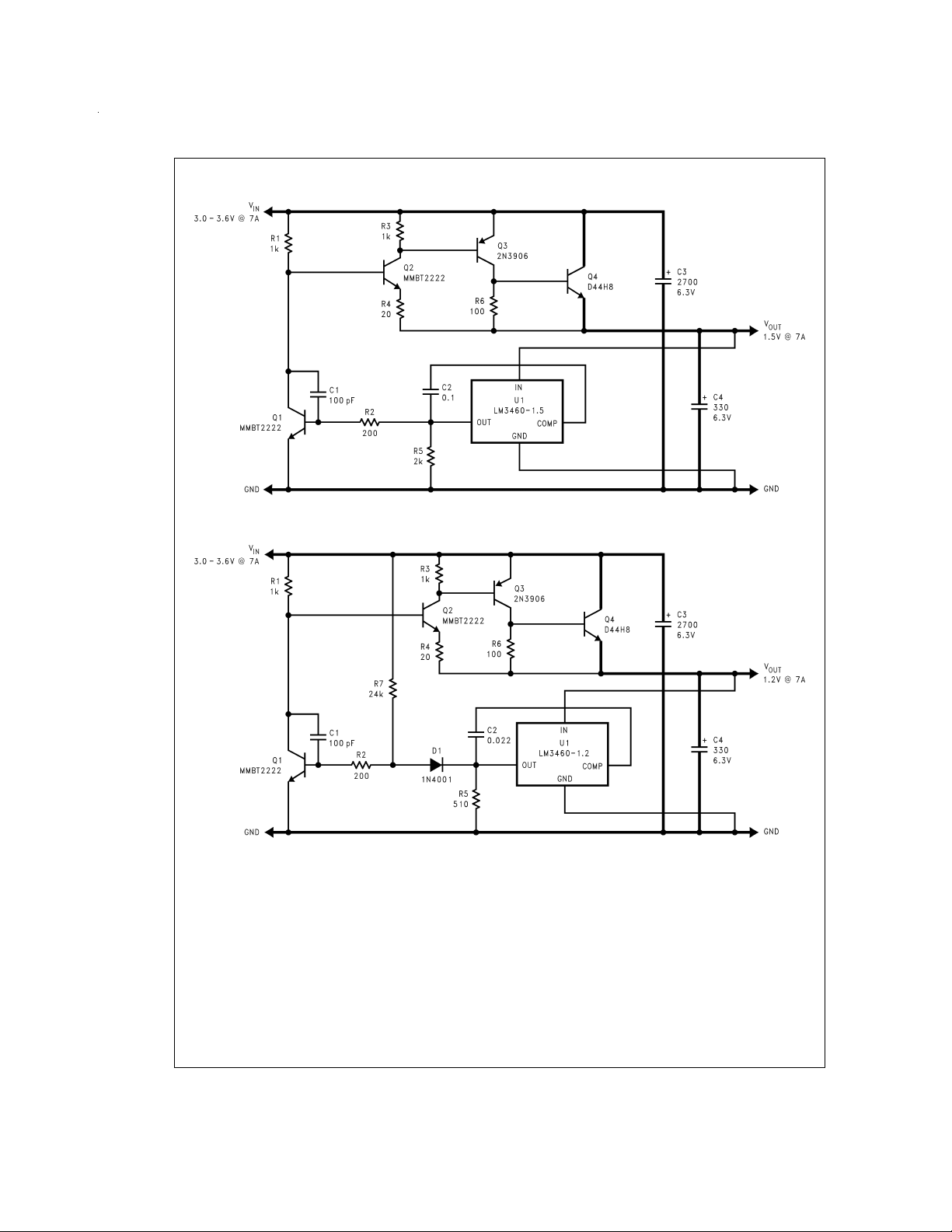
Typical Applications
FIGURE 1. 1.5V Typical Application (See Application Information Section)
DS012603-4
FIGURE 2. 1.2V Typical Application (See Application Information Section)
www.national.com 2
DS012603-5
Page 3
Absolute Maximum Ratings (Note 1)
If Military/Aerospace specified devices are required,
please contact the National Semiconductor Sales Office/
Distributors for availability and specifications.
Input Voltage V
IN
Output Current 20 mA
Junction Temperature 150˚C
Storage Temperature −65˚C to +150˚C
Lead Temperature
Vapor Phase (60 sec.)
Infared (15 sec.)
20V
+215˚C
+220˚C
Power Dissipation (T
(Note 2) 300 mW
ESD Susceptibility (Note 3)
Human Body Model 1500V
See AN-450 ″Surface Mounting Methods and Their Effect
on Product Reliability″ for methods on soldering surface
mount devices.
Operating Ratings (Note 1), (Note 2)
Ambient Temperature Range 0˚C ≤ T
Output Current 1 mA
=
25˚C)
A
≤ +70˚C
A
Electrical Characteristics
LM3460-1.5
Specifications with standard type face are for T
Range. Unless otherwise specified, (+)IN=V
Symbol Parameter Conditions Typ (Note 4) Limit (Note 5) Units
V
REG
I
q
G
m
V
SAT
I
L
R
F
Regulated Voltage I
Regulated Voltage
Tolerance
Quiescent Current I
Transconductance
/ ∆V
∆I
OUT
REG
Output Saturation
Voltage(Note 6)
Output Leakage
Current
Internal Feedback
Resistor (See
OUT
I
OUT
OUT
20µA ≤ I
V
OUT
V
IN
I
OUT
V
IN
V
OUT
Functional Diagram)
E
n
Output Noise Voltage I
OUT
=
25˚C, and those with boldface type apply over full Operating Temperature
J
REG,VOUT
=
1 mA 1.5 1.515/ 1.530
=
200 mV
1.485/1.470
=
1mA
=
1 mA 85 125/150 µA (max)
≤ 1mA
=
=
=
OUT
=
500 mV
V
REG
1mA
V
REG
=
0V
+ 100 mV
− 100 mV
3.3 1/0.5
0.8 0.95 V (max)
0.1 0.5/1.0 µA (max)
7.1
=
1 mA, 10 Hz ≤ f ≤ 10kHz 50 µV (rms)
±1/±
8.9
5.3
2
V (max)
V (min)
%
mA/mV
kΩ(max)
kΩ(min)
(max)
(min)
Electrical Characteristics
LM3460-1.2
Specifications with standard type face are for T
Range. Unless otherwise specified, (+)IN=V
Symbol Parameter Conditions Typ (Note 4) Limit (Note 5) Units
V
REG
I
q
G
m
V
SAT
I
L
R
F
Regulated Voltage I
Regulated Voltage
Tolerance
Quiescent Current I
Transconductance
/ ∆V
∆I
OUT
REG
Output Saturation
Voltage(Note 6)
Output Leakage
Current
Internal Feedback
Resistor (See
OUT
I
OUT
OUT
20µA ≤ I
V
OUT
V
IN
I
OUT
V
IN
V
OUT
Functional Diagram)
E
n
Output Noise Voltage I
OUT
=
25˚C, and those with boldface type apply over full Operating Temperature
J
REG,VOUT
=
1 mA 1.220 1.232/ 1.244
=
200 mV
1.208/1.196
=
1mA
=
1 mA 85 125/150 µA (max)
≤ 1mA
=
=
=
OUT
=
200 mV
V
REG
1mA
V
REG
=
0V
+ 100 mV
− 100 mV
3.3 1/0.5
0.8 0.95 V (max)
0.1 0.5/1.0 µA (max)
10
=
1 mA, 10 Hz ≤ f ≤ 10kHz 50 µV (rms)
±1/±
12.5
7.5
2
www.national.com3
V (max)
V (min)
%
mA/mV
kΩ(max)
kΩ(min)
(max)
(min)
Page 4

Electrical Characteristics
LM3460-1.2
Note 1: Absolute Maximum Ratings are limits beyond which damage to the device may occur. Operating Ratings indicate conditions for which the device is intended
to be functional, but do not guarantee specific performance limits. For guaranteed specifications and test conditions, see the Electrical Characteristics. The guaranteed specifications apply only for the test conditions listed. Some performance characteristics may degrade when the device is not operated under the listed test conditions.
Note 2: The maximum power dissipation must be derated at elevated temperatures and is dictated by T
bient thermal resistance), and T
given in the Absolute Maximum Ratings, whichever is lower. The typical thermal resistance θ
Note 3: The human body model is a 100 pF capacitor discharged through a 1.5 kΩ resistor into each pin.
Note 4: Typical numbers are at 25˚C and represent the most likely parametric norm.
Note 5: Limits are 100%production tested at 25˚C. Limits over the operating temperature range are guaranteed through correlation using Statistical Quality Control
(SQC) methods. The limits are used to calculate National’s Average Outgoing Quality Level (AOQL).
Note 6: V
SAT
=
V
REG−VOUT
(Continued)
(ambient temperature). The maximum allowable power dissipation at any temperature is (P
A
, when the voltage at the IN pin is forced 100mV above the nominal regulating voltage (V
Jmax
when soldered to a printed circuit board is approximately 330˚ C/W.
JA
(maximum junction temperature), θJA(junction ot am-
REG
Dmax
).
=
(T
Jmax−TA
)/θJA) or the number
www.national.com 4
Page 5

Product Description
The LM3460 is a shunt regulator designed for use as a precision control element in a feedback loop. The regulated output voltage is sensed between the IN pin and GROUND pin
of the LM3460.
The output of the LM3460 sources current whenever the
voltage at the IN pin reaches the regulated voltage.
This current is used to cut off the drive to the external pass
trnasistor, which provides the negative feedback to force the
output voltage to be the same value as V
If the voltage on the IN pin is forcedabove the V
the maximum voltage applied to the IN pin should not ex-
REG
.
voltage,
REG
ceed 20V. In addition, an external resistor may be required
on the OUT pin to limit the maximum current to 20 mA.
Compensation
The inverting input of the error amplifier is brought out to simplify closed-loop compensation. Typically, compensation is
provided by a single capacitor connected from the COMPENSATION pin to the OUT pin of the LM3460.
Applying a load pulse to the output of the regulator circuit
and observing the output voltage response is a good method
of verifying the stability of the control loop.
If excessive ringing on the output waveformis observed, this
usually indicates marginal stability resulting from insufficient
phase margin.
Test Circuit
The test circuit shown in
various LM3460 parameters. Test conditions are set by forcing the appropriate voltage at the V
lecting the appropriate R
cal Characteristics section. Use a DVM at the ″measure″ test
points to read the data.
Figure 3
can be used to measure
OUT
or I
as specified in the Electri-
L
OUT
Set test point and se-
V
Set Note: 0V to 500 mV for LM3460-1.5
OUT
0V to 200 mV for LM3460-1.2
FIGURE 3. Test Circuit
Setting the Output Voltage
If a regulated voltage is desired which is not available as a
standard voltage, the output voltage may be adjusted by using an external resistive divider (see
Figure 4
):
DS012603-9
www.national.com5
Page 6

Setting the Output Voltage (Continued)
DS012603-10
PERFORMANCE DATA
All data taken at 20˚C ambient:
LOAD/LINE REGULATION: The output voltage changed
<
0.1 mV as the load was increased from 0-7A,and the input
voltage was varied from 3.0V-3.6V.
DROPOUT VOLTAGE: The dropout voltage (which is de-
fined as the minimum input-output voltage differential required to maintain a regulated output) was measured at 7A
and found to be 1.4V. This means that a minimum input voltage of 2.9V is requiredto keep the 1.5V output in regulation.
TRANSIENT RESPONSE: Transient response was tested
using a 0.2Ω power resistor connected to the output using a
mechanical contact to provide a 0-7A load current step.
When the load was applied, the change in output voltage
Figure 5
<
5 mV with a total recovery time of about 30
).
was seen to be
µs (see
FOR BEST RESULTS: SELECT R
<
500Ω
A
FIGURE 4. Setting the Output Voltage
The simplest way to calculate the resistor values is to assume a value for R
R
.
B
and then solve the equation shown for
A
To assure best output voltage accuracy, the value selected
for R
should be<500Ω, and 1%tolerance resistors should
A
be used.
As the ohmic value of R
divider inside the LM3460 will cause the output voltage to
is increased, the internal resistive
A
deviate from the value predicted by the formula shown.
App Circuit Technical Information
Figure 1
LM3460. This section provides details of circuit function.
1.5V/7A TYPICAL APPLICATION
Figure 1
regulator which provides a regulated 1.5V output at up to 7A
of load current from a 3V-3.6V input.
The pass element of the regulator (which supplies the load
current) is made up of a three-transistor complimentary Darlington composed of Q2, Q3, and Q4. The bias current flowing through R1 will drive the pass element ON, until such
time as Q1 pulls down and takes the drive away from the
base of Q2.
The circuit regulates the output to 1.5V using the LM3460
precision controller, which sources current from its output
whenever the voltage at the IN pin reaches 1.5V.
When the LM3460 sources current from its output, it turns on
Q1 (stealing the base drive for Q2) which reduces the current from the 1.5V regulated output. In this way, a negative
feedback loop is established which locks the output at 1.5V.
C1 and C2 are used for compensation, and should be ceramic capacitors.
C4 is required for regulator stability, and both C3 and C4 affect transient response. Circuit performance should be carefully evaluated if substitutions are made for these two components.
and
Figure 2
highlight two applications of the
shows the schematic of a wide-bandwidth linear
DS012603-11
FIGURE 5. Output Transient Response
HEATSINKING/COMPONENT SELECTION
any
HEATSINKING:As with
linear regulator,the power dissi-
pated in the pass transistor (Q4) is approximately:
P=(V
IN−VOUT
)XI
LOAD
Q4 must be provided with adequate heatsinking so that the
junction temperature never exceeds 150˚C.
Figure 6
shows the maximum allowable values of thermal
resistance (from heatsink-to-ambient) that must be provided
for various values of the load current.
DS012603-12
FIGURE 6. Q4 Heatsink Requirements for Circuit
Shown in
Figure 1
These values are calculated assuming a maximum ambient
of 50˚C, 3.3V input, and a TO-220 power transistor mounted
using thermal grease and a mica insulator.
www.national.com 6
Page 7

App Circuit Technical Information
(Continued)
A given thermal resistance can be obtained by using different combinations of heatsink and airflow (refer to heatsink
manufacturers datasheets).
The design tradeoff here is that heatsinks which are smaller,
lighter, and cheaper require more airflow to get the desired
value of thermal resistance.
TRANSIENT RESPONSE: If the regulator is to respond
quickly to changes in load current demand, the input and
output capacitors must be selected carefully.
The output capacitor C4 is most critical, as it must supply
current to the load in the time it takes the regulator loop to
sense the output voltage change and turn on the pass transistor.A Sanyo Oscon type (or equivalent) will give the best
performance here.
The input capacitor C3 is also important, as it provides an
energy reservoir from which the regulator sources current to
force the output back up to the nominal value. A good, low
ESR electrolytic such as a Panasonic HFQ type is a good
choice for C3.
LAYOUT TIPS: In order to optimize performance, parasitic
inductance due to connecting traces must be minimized. All
paths shown as heavy lines on the schematic must be made
by traces which are wide and short as possible (component
placement should be optimized for minimum lead length).
POWER TRANSISTOR AND DRIVER: The power transistor
used at Q4 must have very good current gain at 7A, and
wide bandwidth (high f
The D44H8 is an excellent choice for cost and performance.
The current gain of Q4 dictates the power dissipation in its
driver (Q3) which must supply the base current to Q4. If the
gain of Q4 is lowered, Q3 must source more current into its
base (and the power dissipation in Q3 goes up proportionately).
The D44H8 has a guaranteed minimum gain of 40
typical gain much higher.Assuming the gain of Q4 is about
30%lower at 7A, it will still be
of load current, Q3 must supply 250 mA to the base of Q4
(worst case).
The power dissipation in Q3 (assuming 3.3V input) will never
exceed approximately 250 mW, which is easily handled by
2N3906 in a TO-92 case (which has a thermal resistance of
about 180˚C/W), but could be a problem for a very smallsurface mount device.
If substitutions are made for Q3 or Q4, careful attention must
be paid to the current gain as well as the f
TRANSISTOR BANDWIDTH: Fast transient response that
the regulator be able to respond quickly to any change in
output voltage (which will occur if the current drawn by the
load suddenly changes).
All of the transistors specified in the schematic are very
wide-band devices (have high f
for fast response. If substitutions are made for any of the
transistors, this specification must be considered.
1.2V/7A TYPICAL APPLICATION
The 1.2V
@
7A design in
to the design shown in
tions previously detailed for that circuit apply unchanged to
Figure 2
, will not be repeated.
) for this circuit to work as specified.
T
@
4A, with
>
28. Therefore, to support7A
.
T
values) which is necessary
T
Figure 2
Figure 1
is very similar in function
. Most of the circuit descrip-
Detailed information will be presented in the areas which differ between the two circuits.
HEATSINKING
The 1.2V design needs a little more heatsinking because the
lower output voltage means more power dissipation in Q4 at
any value of load current.
Figure 7
shows the maximum allowable values of thermal
resistance (from heatsink-to-ambient) that must be provided
for various values of the load current.
DS012603-13
FIGURE 7. Q4 Heatsink Requirements for Circuit
shown in
Figure 2
Q1 DRIVE CIRCUITRY
Figure 1
In the circuit shown in
base of Q1 with current when the voltage at V
the regulation point.As Q1 turns ON, it steals drive from Q2
, the output of U1 drives the
reaches
OUT
which holds the loop in regulation.
The circuit of
Figure 2
uses a different drive configuration for
Q1, required because of the lower voltage across U1.
With only 1.2V across U1, the OUT pin of the LM3460 can-
not swing up high enough in voltage to turn on the V
Figure 2
In the circuit of
only when U1 sources current:
, drive for Q1 is provided by R7,
The operation of the drive
BE
of Q1.
but
scheme is as follows:
If the voltage at V
the OUT pin of U1. Q1 is held OFF as the current flowing
is below 1.2V, no current flows from
OUT
down through R7 goes through D1 and R5 to ground.
IMPORTANT: Diode D1 is a 1N4001 becauseits V
much less than the V
not work here).
of Q1 (a signal diode like 1N4148 will
BE
must be
F
When U1 is not sourcing current, the voltage at the OUT pin
(and the cathode of D1) will be held at about 50 mV by the
R7/D1/R5 divider. The current flowing to ground through
these components is about 110 µA.
Because D1 is a 1A power diode, the V
small value of current will be much less than the V
to turn ON Q1 (so Q1 is held off by D1).
across D1 at this
F
BE
needed
When U1 begins to source current (to cut off the pass transistor and regulate V
of D1 to rise.
) it forces the voltage at the cathode
OUT
This action causes the current that was flowing through D1
to flow into the base of Q1, turning it ON and taking drive
away from the base of Q2.
This action provides the negative feedback required to regulate V
of total supply voltage across the device.
and allows the LM3460 to operate with only 1.2V
OUT
www.national.com7
Page 8

Physical Dimensions inches (millimeters) unless otherwise noted
5-Lead Small Outline Package (M5)
Order Number, See Ordering Information Table
NS Package Number MA05B
LIFE SUPPORT POLICY
LM3460-1.2, -1.5 Precision Controller for GTLp and GTL Bus Termination
NATIONAL’S PRODUCTS ARE NOT AUTHORIZED FOR USE AS CRITICAL COMPONENTS IN LIFE SUPPORT
DEVICES OR SYSTEMS WITHOUT THE EXPRESS WRITTEN APPROVAL OF THE PRESIDENT AND GENERAL
COUNSEL OF NATIONAL SEMICONDUCTOR CORPORATION. As used herein:
1. Life support devices or systems are devices or
systems which, (a) are intended for surgical implant
into the body, or (b) support or sustain life, and
whose failure to perform when properly used in
accordance with instructions for use provided in the
2. A critical component is any component of a life
support device or system whose failure to perform
can be reasonably expected to cause the failure of
the life support device or system, or to affect its
safety or effectiveness.
labeling, can be reasonably expected to result in a
significant injury to the user.
National Semiconductor
Corporation
Americas
Tel: 1-800-272-9959
Fax: 1-800-737-7018
Email: support@nsc.com
www.national.com
National does not assume any responsibility for use of any circuitry described, no circuit patent licenses are implied and National reserves the right at any time without notice to change said circuitry and specifications.
National Semiconductor
Europe
Fax: +49 (0) 1 80-530 85 86
Email: europe.support@nsc.com
Deutsch Tel: +49 (0) 1 80-530 85 85
English Tel: +49 (0) 1 80-532 78 32
Français Tel: +49 (0) 1 80-532 93 58
Italiano Tel: +49 (0) 1 80-534 16 80
National Semiconductor
Asia Pacific Customer
Response Group
Tel: 65-2544466
Fax: 65-2504466
Email: sea.support@nsc.com
National Semiconductor
Japan Ltd.
Tel: 81-3-5639-7560
Fax: 81-3-5639-7507
 Loading...