

Page 1
TL/H/7785
LM145/LM345 Negative Three Amp Regulator
January 1995
LM145/LM345 Negative Three Amp Regulator
General Description
The LM145 is a three-terminal negative regulator with a
fixed output voltage of
b
5V and up to 3A load current capability. This device needs only one external componentÐa
compensation capacitor at the output, making it easy to apply. Worst case guarantees on output voltage deviation due
to any combination of line, load or temperature variation
assure satisfactory system operation.
Exceptional effort has been made to make the LM145 immune to overload conditions. The regulator has current limiting which is independent of temperature, combined with
thermal overload protection. Internal current limiting protects against momentary faults while thermal shutdown prevents junction temperatures from exceeding safe limits during prolonged overloads.
Although primarily intended for fixed output voltage applications, the LM145 may be programmed for higher output voltages with a simple resistive divider. The low quiescent drain
current of the device allows this technique to be used with
good regulation.
The LM145 comes in a hermetic TO-3 package rated at
25W. A reduced temperature range part LM345 is also available.
Features
Y
Output voltage accurate to better thang2%
Y
Current limit constant with temperature
Y
Internal thermal shutdown protection
Y
Operates with input-output voltage differential of 2.8V at
full rated load over full temperature range
Y
Regulation guaranteed with 25W power dissipation
Y
3A output current guaranteed
Y
Only one external component needed
Y
PaProduct Enhancement tested
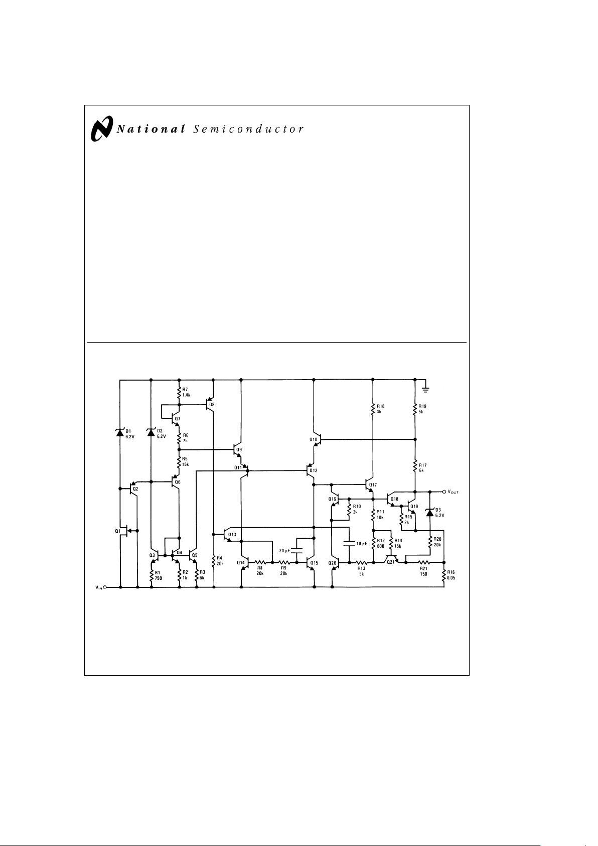
Schematic Diagram
TL/H/7785– 1
C
1995 National Semiconductor Corporation RRD-B30M115/Printed in U. S. A.
Page 2
Absolute Maximum Ratings
If Military/Aerospace specified devices are required,
please contact the National Semiconductor Sales
Office/Distributors for availability and specifications.
(Note 3)
Input Voltage 20V
Input-Output Differential 20V
Power Dissipation Internally Limited
Operating Junction Temperature Range
LM145
b
55§Ctoa150§C
LM345 0
§
Ctoa125§C
Storage Temperature Range
b
65§Ctoa150§C
Lead Temperature (Soldering, 10 sec.) 300
§
C
Electrical Characteristics (Note 1)
Limits
Parameter Conditions LM145 LM345 Units
Min Typ Max Min Typ Max
Output Voltage T
j
e
25§C, I
OUT
e
5 mA,
b
5.1
b
5.0
b
4.9
b
5.2
b
5.0
b
4.8 V
V
IN
eb
7.5
Line Regulation (Note 2) T
j
e
25§C
5 15 5 25 mV
b
20VsV
IN
s
b
7.5V
Load Regulation (Note 2) T
j
e
25§C, V
IN
eb
7.5V
30 75 30 100 mV
5mAsI
OUT
s
3A
Output Voltage
b
20VsV
IN
s
b
7.8V
5mA
s
I
OUT
s
3A
P
s
25W
b
5.20
b
4.80b5.25
b
4.75 V
T
MIN
s
T
j
s
T
MAX
Quiescent Current
b
20VsV
IN
s
b
7.5V
1.0 3.0 1.0 3.0 mA
5mA
s
I
OUT
s
3A
Short Circuit Current V
IN
eb
7.5V, T
j
ea
25§C 4 5.5 4 5.5 A
V
IN
eb
20V, T
j
ea
25§C 2 3.5 2 3.5 A
Output Noise Voltage T
A
e
25§C, C
L
e
4.7 mF
150 150 mV
10 Hz
sfs
100 kHz
Long Term Stability 5 50 5 50 mV
Thermal Resistance
22
§
C/W
Junction to Case
Note 1: Unless otherwise specified, these specifications apply:b55§CsT
j
s
a
150§C for the LM145 and 0§CsT
j
s
a
125§C for the LM345. V
IN
e
7.5V and
I
OUT
e
5 mA. Although power dissipation is internally limited, electrical specifications apply only for power levels up to 25W. For calculations of junction
temperature rise due to power dissipation, use a thermal resistance of 35
§
C/W for the TO-3 with no heat sink. With a heat sink, use 2§C/W for junction to case
thermal resistance.
Note 2: Regulation is measured at constant junction temperature. Changes in output voltage due to heating effects must be taken into account separately. To
ensure constant junction temperature, pulse testing with a low duty cycle is used.
Note 3: Refer to RETS145K-5V for LM145K-5.0 military specifications.
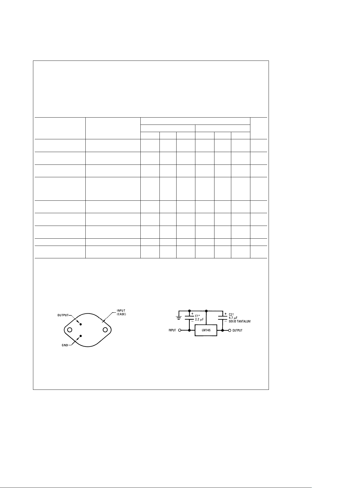
Connection Diagram
Metal Can Package
TL/H/7785– 2
Bottom View
Order Number LM345K-5.0
See NS Package Number K02A
Order Number LM145K-5.0/883 or
SMD
Ý
5962-9064501
See NS Package Number K02C
Typical Applications
Fixed Regulator
TL/H/7785– 3
²
Required for stability. For value given, capacitor must be solid tantalum.
50 mF aluminum electrolytic may be substituted. Values given may be increased without limit.
*Required if regulator is separated from filter capacitor. For value given, ca-
pacitor must be solid tantulum. 50 mF aluminum electrolytic may be substituted.
2
Page 3

Typical Performance Characteristics
Dissipation for LM145
Maximum Average Power
Dissipation for LM345
Maximum Average Power
Ripple Rejection
Output Impedance Voltage Differential
Minimum Input-Output
Temperature
Output Voltage vs
TL/H/7785– 4
Typical Applications (Continued)
TL/H/7785– 5
*Select resistors to set output voltage. 1 ppm/C tracking suggested.
**C1 is not needed if power supply filter capacitor is within 3
×
of regulator.
²
Determines zener current. May be adjusted to minimize temperature drift.
²²
Solid tantalum.
Load and line regulation
k
0.01%
Temperature drift
k
0.001%/C
3
Page 4

Typical Applications (Continued)
High Stability Regulator
TL/H/7785– 6
**C1 is not needed if power supply filter capacitor is within 3×of regulator.
²
Keep C4 within 2×of LM345.
**D2 sets initial output voltage accuracy. The LM113 is available in
b5,b
2, andb1% tolerance.
b
2V ECL Termination Regulator
Dual 3 Amp Trimmed Supply
TL/H/7785– 7
Variable Output (b5.0V tob15V)
TL/H/7785– 8
*Optional. Improves transient
V
OUT
eb
5V
#
R1aR2
R2
J
response and ripple rejection.
4
Page 5

Physical Dimensions inches (millimeters)
Metal Can Package (K)
Order Number LM345K-5.0
NS Package Number K02A
5
Page 6

LM145/LM345 Negative Three Amp Regulator
Physical Dimensions inches (millimeters) (Continued)
Metal Can Package (K)
Mil-Aero Products
Order Number LM145K-5.0/883 or SMD
Ý
5962-9064501
NS Package Number K02C
LIFE SUPPORT POLICY
NATIONAL’S PRODUCTS ARE NOT AUTHORIZED FOR USE AS CRITICAL COMPONENTS IN LIFE SUPPORT
DEVICES OR SYSTEMS WITHOUT THE EXPRESS WRITTEN APPROVAL OF THE PRESIDENT OF NATIONAL
SEMICONDUCTOR CORPORATION. As used herein:
1. Life support devices or systems are devices or 2. A critical component is any component of a life
systems which, (a) are intended for surgical implant support device or system whose failure to perform can
into the body, or (b) support or sustain life, and whose be reasonably expected to cause the failure of the life
failure to perform, when properly used in accordance support device or system, or to affect its safety or
with instructions for use provided in the labeling, can effectiveness.
be reasonably expected to result in a significant injury
to the user.
National Semiconductor National Semiconductor National Semiconductor National Semiconductor
Corporation Europe Hong Kong Ltd. Japan Ltd.
1111 West Bardin Road Fax: (
a
49) 0-180-530 85 86 13th Floor, Straight Block, Tel: 81-043-299-2309
Arlington, TX 76017 Email: cnjwge@tevm2.nsc.com Ocean Centre, 5 Canton Rd. Fax: 81-043-299-2408
Tel: 1(800) 272-9959 Deutsch Tel: (
a
49) 0-180-530 85 85 Tsimshatsui, Kowloon
Fax: 1(800) 737-7018 English Tel: (
a
49) 0-180-532 78 32 Hong Kong
Fran3ais Tel: (
a
49) 0-180-532 93 58 Tel: (852) 2737-1600
Italiano Tel: (
a
49) 0-180-534 16 80 Fax: (852) 2736-9960
National does not assume any responsibility for use of any circuitry described, no circuit patent licenses are implied and National reserves the right at any time without notice to change said circuitry and specifications.
 Loading...