

Datasheet LM3420M5-16.8, LM3420M5-12.6, LM3420AM5X-4.2, LM3420AM5X-16.8, LM3420AM5-8.4 Datasheet (NSC)
...Page 1
LM3420-4.2, -8.2, -8.4, -12.6, -16.8
Lithium-Ion Battery Charge Controller
General Description
The LM3420 series of controllers are monolithic integrated
circuits designed for charging and end-of-charge control for
Lithium-Ion rechargeable batteries. The LM3420 is available
in fivefixedvoltage versions for one through four cell charger
applications (4.2V, 8.2V/8.4V, 12.6V and 16.8V respectively).
Included in a very small package is an (internally compensated) op amp, a bandgap reference, an NPN output transistor, and voltage setting resistors. The amplifier’s inverting input is externally accessible for loop frequency
compensation. The output is an open-emitter NPN transistor
capable of driving up to 15 mA of output current into external
circuitry.
A trimmed precision bandgap reference utilizes temperature
drift curvature correction for excellent voltage stability over
the operating temperature range. Available with an initial tolerance of 0.5%for the A grade version, and 1%for the standard version, the LM3420 allows for precision end-of-charge
control for Lithium-Ion rechargeable batteries.
The LM3420 is available in a sub-miniature 5-lead SOT23-5
surface mount package thus allowing very compact designs.
Features
n Voltage options for charging 1, 2, 3 or 4 cells
n Tiny SOT23-5 package
n Precision (0.5%) end-of-charge control
n Drive capability for external power stage
n Low quiescent current, 85 µA (typ.)
Applications
n Lithium-Ion battery charging
n Suitable for linear and switching regulator charger
designs
LM3420-4.2, -8.2, -8.4, -12.6, -16.8 Lithium-Ion Battery Charge Controller
May 1998
Typical Application and Functional Diagram
DS012359-1
Typical Constant Current/Constant Voltage
SIMPLE SWITCHER®is a registered trademark of National Semiconductor Corporation.
© 1999 National Semiconductor Corporation DS012359 www.national.com
Li-Ion Battery Charger
DS012359-2
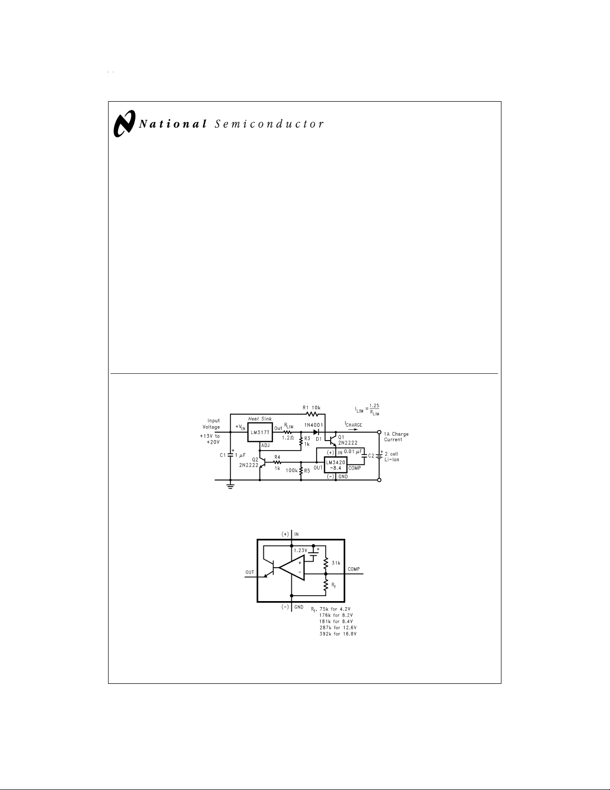
LM3420 Functional Diagram
Page 2
Connection Diagrams and Order Information
5-Lead Small Outline Package (M5)
Actual Size
DS012359-4
*No internal connection, but should be soldered to PC board for best heat
transfer.
DS012359-3
Top View
For Ordering Information
See
Figure 1
See NS Package Number MA05B
in this Data Sheet
www.national.com 2
Page 3
Absolute Maximum Ratings (Note 1)
If Military/Aerospace specified devices are required,
please contact the National Semiconductor Sales Office/
Distributors for availability and specifications.
Input Voltage V(IN) 20V
Output Current 20 mA
Junction Temperature 150˚C
Storage Temperature −65˚C to +150˚C
Lead Temperature
Vapor Phase (60 seconds) +215˚C
ESD Susceptibility (Note 3)
Human Body Model 1500V
See AN-450 “Surface Mounting Methods and Their Effect
on Product Reliability” for methods on soldering
surface-mount devices.
Operating Ratings (Notes 1, 2)
Ambient Temperature Range −40˚C ≤ T
Junction Temperature Range −40˚C ≤ T
Output Current 15 mA
≤ +85˚C
A
≤ +125˚C
J
Infrared (15 seconds) +220˚C
=
Power Dissipation (T
(Note 2) 300 mW
25˚C)
A
LM3420-4.2
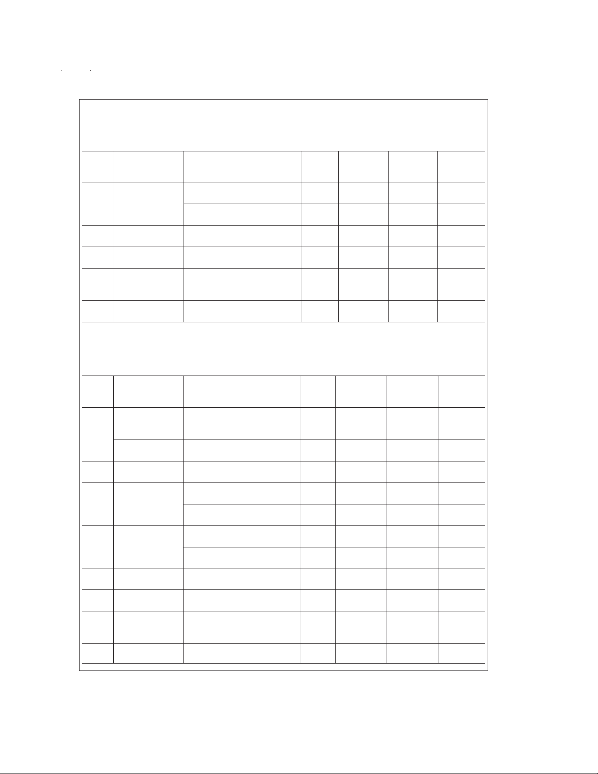
Electrical Characteristics
Specifications with standard type face are for T
ture Range. Unless otherwise specified, V(IN)=V
Symbol Parameter Conditions Typical LM3420A-4.2 LM3420-4.2 Units
V
REG
Regulation Voltage I
Regulation Voltage I
OUT
OUT
=
=
Tolerance
I
q
G
Quiescent Current I
Transconductance 20 µA ≤ I
m
∆I
/∆V
OUT
REG
=
OUT
=
V
OUT
1mA≤I
=
V
A
V
Voltage Gain 1V ≤ V
∆V
/∆V
OUT
REG
OUT
=
R
200Ω (Note 6) 550/250 450/200 V/V(min)
L
1V ≤ V
=
R
2kΩ 1500/900 1000/700 V/V(min)
OUT
L
OUT
=
=
V
SAT
Output Saturation V(IN)=V
(Note 7) I
I
L
Output Leakage V(IN)=V
Current V
R
f
Internal Feedback 75 kΩ
Resistor (Note 8) 94 94 kΩ(max)
E
n
Output Noise I
OUT
=
Voltage
=
25˚C, and those with boldface type apply over full Operating Tempera-
J
REG,VOUT
=
1.5V.
(Note 4) Limit Limit (Limits)
(Note 5) (Note 5)
1 mA 4.2 V
4.221/4.242 4.242/4.284 V(max)
4.179/4.158 4.158/4.116 V(min)
1mA
±
0.5/±1
±1/±
2
%
(max)
1mA 85 µA
110/115 125/150 µA(max)
≤ 1 mA 3.3 mA/mV
OUT
2V 1.3/0.75 1.0/0.50 mA/mV(min)
≤ 15 mA 6.0 mA/mV
OUT
2V 3.0/1.5 2.5/1.4 mA/mV(min)
≤ V
OUT
OUT
REG
− 1.2V (−1.3) 1000 V/V
REG
≤ V
− 1.2V (−1.3) 3500 V/V
REG
+100 mV 1.0 V
15 mA 1.2/1.3 1.2/1.3 V(max)
−100 mV 0.1 µA
REG
0V 0.5/1.0 0.5/1.0 µA(max)
56 56 kΩ(min)
1 mA, 10 Hz ≤ f ≤ 10 kHz 70 µV
RMS
www.national.com3
Page 4
LM3420-8.2
Electrical Characteristics
Specifications with standard type face are for T
ture Range. Unless otherwise specified, V(IN)=V
Symbol Parameter Conditions Typical LM3420A-8.2 LM3420-8.2 Units
V
REG
Regulation Voltage I
Regulation Voltage I
OUT
OUT
=
=
Tolerance
I
q
G
Quiescent Current I
Transconductance 20 µA ≤ I
m
∆I
/∆V
OUT
REG
=
OUT
=
V
OUT
1mA≤I
=
V
A
V
Voltage Gain 1V ≤ V
∆V
/∆V
OUT
REG
OUT
=
R
470Ω (Note 6) 550/250 450/200 V/V(min)
L
1V ≤ V
=
R
5kΩ 1500/900 1000/700 V/V(min)
OUT
L
OUT
=
=
V
SAT
Output Saturation V(IN)=V
(Note 7) I
I
L
Output Leakage V(IN)=V
Current V
R
f
Internal Feedback 176 kΩ
Resistor (Note 8) 220 220 kΩ(max)
E
n
Output Noise I
OUT
=
Voltage
=
25˚C, and those with boldface type apply over full Operating Tempera-
J
REG,VOUT
=
1.5V.
(Note 4) Limit Limit (Limits)
(Note 5) (Note 5)
1 mA 8.2 V
8.241/8.282 8.282/8.364 V(max)
8.159/8.118 8.118/8.036 V(min)
1mA
±
0.5/±1
±1/±
2
%
(max)
1mA 85 µA
110/115 125/150 µA(max)
≤ 1 mA 3.3 mA/mV
OUT
6V 1.3/0.75 1.0/0.50 mA/mV(min)
≤ 15 mA 6.0 mA/mV
OUT
6V 3.0/1.5 2.5/1.4 mA/mV(min)
≤ V
OUT
OUT
REG
− 1.2V (−1.3) 1000 V/V
REG
≤ V
− 1.2V (−1.3) 3500 V/V
REG
+100 mV 1.0 V
15 mA 1.2/1.3 1.2/1.3 V(max)
−100 mV 0.1 µA
REG
0V 0.5/1.0 0.5/1.0 µA(max)
132 132 kΩ(min)
1 mA, 10 Hz ≤ f ≤ 10 kHz 140 µV
RMS
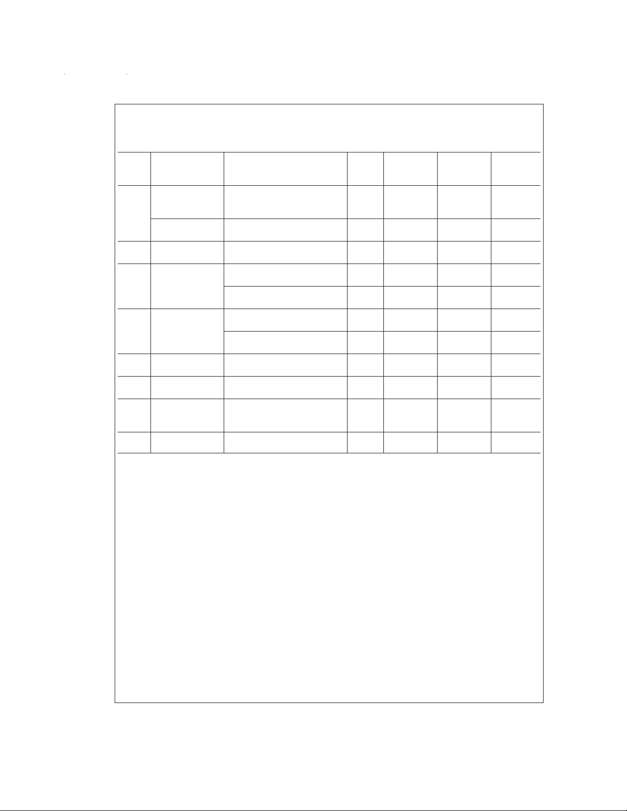
LM3420-8.4
Electrical Characteristics
Specifications with standard type face are for T
ture Range. Unless otherwise specified, V(IN)=V
Symbol Parameter Conditions Typical LM3420A-8.4 LM3420-8.4 Units
V
REG
Regulation Voltage I
Regulation Voltage I
OUT
OUT
=
=
Tolerance
I
q
G
Quiescent Current I
Transconductance 20 µA ≤ I
m
∆I
/∆V
OUT
REG
=
OUT
=
V
OUT
1mA≤I
=
V
OUT
www.national.com 4
=
25˚C, and those with boldface type apply over full Operating Tempera-
J
REG,VOUT
=
1.5V.
(Note 4) Limit Limit (Limits)
(Note 5) (Note 5)
1 mA 8.4 V
8.442/8.484 8.484/8.568 V(max)
8.358/8.316 8.316/8.232 V(min)
1mA
±
0.5/±1
±1/±
2
%
1mA 85 µA
110/115 125/150 µA(max)
≤ 1 mA 3.3 mA/mV
OUT
6V 1.3/0.75 1.0/0.50 mA/mV(min)
≤ 15 mA 6.0 mA/mV
OUT
6V 3.0/1.5 2.5/1.4 mA/mV(min)
(max)
Page 5
LM3420-8.4
Electrical Characteristics
Specifications with standard type face are for T
ture Range. Unless otherwise specified, V(IN)=V
Symbol Parameter Conditions Typical LM3420A-8.4 LM3420-8.4 Units
A
V
V
SAT
I
L
R
f
E
n
Voltage Gain 1V ≤ V
∆V
OUT
/∆V
REG
R
L
1V ≤ V
R
L
Output Saturation V(IN)=V
(Note 7) I
OUT
Output Leakage V(IN)=V
Current V
OUT
Internal Feedback 181 kΩ
Resistor (Note 8) 227 227 kΩ(max)
Output Noise I
OUT
Voltage
(Continued)
=
25˚C, and those with boldface type apply over full Operating Tempera-
J
REG,VOUT
=
1.5V.
(Note 4) Limit Limit (Limits)
(Note 5) (Note 5)
≤ V
OUT
=
470Ω (Note 6) 550/250 450/200 V/V(min)
OUT
=
5kΩ 1500/900 1000/700 V/V(min)
=
15 mA 1.2/1.3 1.2/1.3 V(max)
=
0V 0.5/1.0 0.5/1.0 µA(max)
− 1.2V (−1.3) 1000 V/V
REG
≤ V
− 1.2V (−1.3) 3500 V/V
REG
+100 mV 1.0 V
REG
−100 mV 0.1 µA
REG
135 135 kΩ(min)
=
1 mA, 10 Hz ≤ f ≤ 10 kHz 140 µV
RMS
LM3420-12.6
Electrical Characteristics
Specifications with standard type face are for T
Range. Unless otherwise specified, V(IN)=V
Symbol Parameter Conditions Typical LM3420A-12.6 LM3420-12.6 Units
V
REG
Regulation Voltage I
Regulation Voltage I
OUT
OUT
=
=
Tolerance
I
q
G
m
Quiescent Current I
Transconductance 20 µA ≤ I
∆I
/∆V
OUT
REG
=
OUT
=
V
OUT
1mA≤I
=
V
A
V
Voltage Gain 1V ≤ V
∆V
/∆V
OUT
REG
OUT
=
R
750Ω (Note 6) 550/250 450/200 V/V(min)
L
1V ≤ V
=
R
10 kΩ 1500/900 1000/700 V/V(min)
OUT
L
OUT
=
=
V
SAT
Output Saturation V(IN)=V
(Note 7) I
I
L
Output Leakage V(IN)=V
Current V
R
f
Internal Feedback 287 kΩ
Resistor (Note 8) 359 359 kΩ(max)
E
n
Output Noise
Voltage
=
I
OUT
=
25˚C, and those with boldface type apply over full Operating Temperature
J
REG,VOUT
=
1.5V.
(Note 4) Limit Limit (Limits)
(Note 5) (Note 5)
1 mA 12.6 V
12.663/12.726 12.726/12.852 V(max)
12.537/12.474 12.474/12.348 V(min)
1mA
±
0.5/±1
±1/±
2
%
(max)
1mA 85 µA
110/115 125/150 µA(max)
≤ 1 mA 3.3 mA/mV
OUT
10V 1.3/0.75 1.0/0.5 mA/mV(min)
≤ 15 mA 6.0 mA/mV
OUT
10V 3.0/1.5 2.5/1.4 mA/mV(min)
≤ V
OUT
OUT
REG
− 1.2V (−1.3) 1000 V/V
REG
≤ V
− 1.2V (−1.3) 3500 V/V
REG
+100 mV 1.0 V
15 mA 1.2/1.3 1.2/1.3 V(max)
−100 mV 0.1 µA
REG
0V 0.5/1.0 0.5/1.0 µA(max)
215 215 kΩ(min)
1 mA, 10 Hz ≤ f ≤ 10 kHz
210 µV
RMS
www.national.com5
Page 6
LM3420-16.8
Electrical Characteristics
Specifications with standard type face are for T
Range. Unless otherwise specified, V(IN)=V
Symbol Parameter Conditions Typical LM3420A-16.8 LM3420-16.8 Units
V
Regulation Voltage I
REG
Regulation Voltage I
OUT
OUT
=
=
Tolerance
I
q
G
Quiescent Current I
Transconductance 20 µA ≤ I
m
∆I
/∆V
OUT
REG
=
OUT
=
V
OUT
1mA≤I
=
V
A
Voltage Gain 1V ≤ V
V
∆V
/∆V
OUT
REG
OUT
=
R
1kΩ(Note 6) 550/250 450/200 V/V(min)
L
1V ≤ V
=
R
15 kΩ 1200/750 1000/650 V/V(min)
OUT
L
OUT
=
=
V
Output Saturation V(IN)=V
SAT
(Note 7) I
I
L
Output Leakage V(IN)=V
Current V
R
Internal Feedback 392 kΩ
f
Resistor (Note 8) 490 490 kΩ(max)
E
Output Noise
n
Voltage
Note 1: Absolute Maximum Ratings indicate limits beyond which damage to the device may occur. Operating Ratings indicate conditions for which the device is intended to be functional, but do not guarantee specific performance limits. For guaranteed specifications and test conditions, see the Electrical Characteristics. The
guaranteed specifications apply only for the test conditions listed. Some performance characteristics may degrade when the device is not operated under the listed
test conditions.
Note 2: The maximum power dissipation must be derated at elevated temperatures and is dictated by T
bient thermal resistance), and T
given in the Absolute Maximum Ratings, whichever is lower. The typical thermal resistance (θ
for the M5 package.
Note 3: The human body model is a 100 pF capacitor discharged through a 1.5 kΩ resistor into each pin.
Note 4: Typical numbers are at 25˚C and represent the most likely parametric norm.
Note 5: Limits are 100%production tested at 25˚C. Limits over the operating temperature range are guaranteed through correlation using Statistical Quality Control
(SQC) methods. The limits are used to calculate National’s Averaging Outgoing Quality Level (AOQL).
Note 6: Actual test is done using equivalent current sink instead of a resistor load.
Note 7: V
Note 8: See Applications and Typical Performance Characteristics sections for information on this resistor.
SAT
=
V(IN) − V
(ambient temperature). The maximum allowable power dissipation at any temperature is P
A
, when the voltage at the IN pin is forced 100 mV above the nominal regulating voltage (V
OUT
=
I
OUT
=
25˚C, and those with boldface type apply over full Operating Temperature
J
REG,VOUT
=
1.5V.
(Note 4) Limit Limit (Limits)
(Note 5) (Note 5)
1 mA 16.8 V
16.884/16.968 16.968/17.136 V(max)
16.716/16.632 16.632/16.464 V(min)
1mA
±
0.5/±1
±1/±
2
%
(max)
1mA 85 µA
110/115 125/150 µA(max)
≤ 1 mA 3.3 mA/mV
OUT
15V 0.8/0.4 0.7/0.35 mA/mV(min)
≤ 15 mA 6.0 mA/mV
OUT
15V 2.9/0.9 2.5/0.75 mA/mV(min)
≤ V
OUT
OUT
REG
− 1.2V (−1.3) 1000 V/V
REG
≤ V
− 1.2V (−1.3) 3500 V/V
REG
+100 mV 1.0 V
15 mA 1.2/1.3 1.2/1.3 V(max)
−100 mV 0.1 µA
REG
0V 0.5/1.0 0.5/1.0 µA(max)
294 294 kΩ(min)
1 mA, 10 Hz ≤ f ≤ 10 kHz
280 µV
(maximum junction temperature), θJA(junction to am-
Jmax
) when soldered to a printed circuit board is approximately 306˚C/W
JA
REG
Dmax
).
=
(T
Jmax−TA
)/θJAor the number
RMS
www.national.com 6
Page 7

Typical Performance Characteristics
4.2V
Bode Plot
8.2V and 8.4V
Bode Plot
12.6V
Bode Plot
DS012359-17
DS012359-20
Response Time
for 4.2V Version
Response Time for
8.2V, 8.4V Versions
Response Time
for 12.6V Version
DS012359-18
DS012359-21
Response Time
for 4.2V Version
DS012359-19
Response Time for
8.2V, 8.4V Versions
DS012359-22
Response Time
for 12.6V Version
16.8V
Bode Plot
DS012359-23
DS012359-26
Response Time
for 16.8V Version
DS012359-24
DS012359-27
DS012359-25
Response Time
for 16.8V Version
DS012359-28
www.national.com7
Page 8

Typical Performance Characteristics (Continued)
Regulation Voltage vs
Output Voltage and
Load Resistance
Regulation Voltage vs
Output Voltage and
Load Resistance
DS012359-29
DS012359-32
Circuit Used for Bode Plots
Quiescent Current
DS012359-30
DS012359-33
Circuit Used for Response Time
DS012359-31
Internal Feedback
Resistor (Rf)
Tempco
DS012359-34
Regulation Voltage vs
Output Voltage and
Load Resistance
DS012359-35
www.national.com 8
Normalized
Temperature Drift
DS012359-36
Output Saturation
Voltage (V
SAT
)
DS012359-37
Page 9

Typical Performance Characteristics (Continued)
Regulation Voltage vs
Output Voltage and
Load Resistance
DS012359-38
www.national.com9
Page 10

Five Lead Surface Mount Package Information
The small SOT23-5 package allows only 4 alphanumeric characters to identify the product. The table below contains the field information marked on the package.
Voltage Grade Order Package Supplied as
Information Marking
4.2V A (Prime) LM3420AM5-4.2 D02A 250 unit increments on tape and reel
4.2V A (Prime) LM3420AM5X-4.2 D02A 3k unit increments on tape and reel
4.2V B (Standard) LM3420M5-4.2 D02B 250 unit increments on tape and reel
4.2V B (Standard) LM3420M5X-4.2 D02B 3k unit increments on tape and reel
8.2V A (Prime) LM3420AM5-8.2 D07A 250 unit increments on tape and reel
8.2V A (Prime) LM3420AM5X-8.2 D07A 3k unit increments on tape and reel
8.2V B (Standard) LM3420M5-8.2 D07B 250 unit increments on tape and reel
8.2V B (Standard) LM3420M5X-8.2 D07B 3k unit increments on tape and reel
8.4V A (Prime) LM3420AM5-8.4 D03A 250 unit increments on tape and reel
8.4V A (Prime) LM3420AM5X-8.4 D03A 3k unit increments on tape and reel
8.4V B (Standard) LM3420M5-8.4 D03B 250 unit increments on tape and reel
8.4V B (Standard) LM3420M5X-8.4 D03B 3k unit increments on tape and reel
12.6V A (Prime) LM3420AM5-12.6 D04A 250 unit increments on tape and reel
12.6V A (Prime) LM3420AM5X-12.6 D04A 3k unit increments on tape and reel
12.6V B (Standard) LM3420M5-12.6 D04B 250 unit increments on tape and reel
12.6V B (Standard) LM3420M5X-12.6 D04B 3k unit increments on tape and reel
16.8V A (Prime) LM3420AM5-16.8 D05A 250 unit increments on tape and reel
16.8V A (Prime) LM3420AM5X-16.8 D05A 3k unit increments on tape and reel
16.8V B (Standard) LM3420M5-16.8 D05B 250 unit increments on tape and reel
16.8V B (Standard) LM3420M5X-16.8 D05B 3k unit increments on tape and reel
FIGURE 1. SOT23-5 Marking
The first letter “D” identifies the part as a Driver, the next two numbers indicate the voltage, “02” for a 4.2V part, “07” for an 8.2V
part, “03” for an 8.4V part, “04” for a 12.6V part, and “05” for a 16.8V part. The fourth letter indicates the grade, “B” for standard
grade, “A” for the prime grade.
The SOT23-5 surface mount package is only available on tape in quantity increments of 250 on tape and reel (indicated by the
letters “M5” in the part number), or in quantity increments of 3000 on tape and reel (indicated by the letters “M5X” in the part number).
Product Description
The LM3420 is a shunt regulator specifically designed to be
the reference and control section in an overall feedback loop
of a Lithium-Ion battery charger. The regulated output voltage is sensed between the IN pin and GROUND pin of the
LM3420. If the voltage at the IN pin is less than the LM3420
regulating voltage (V
As the voltage at the IN pin approaches the V
the OUT pin begins sourcing current. This current is then
), the OUT pin sources no current.
REG
REG
voltage,
used to drive a feedback device (opto-coupler), or a power
device (linear regulator, switching regulator, etc.), which servos the output voltage to be the same value as V
REG
.
In some applications, (even under normal operating conditions) the voltage on the IN pin can be forced above the
V
voltage. In these instances, the maximum voltage ap-
REG
plied to the IN pin should not exceed 20V. In addition, an external resistor may be required on the OUT pin to limit the
maximum current to 20 mA.
Compensation
The inverting input of the error amplifier is brought out to allow overall closed-loop compensation. In many of the applications circuits shown here, compensation is provided by a
single capacitor (C
to the out pin of the LM3420. The capacitor values shown in
the schematics are adequate under most conditions, but
they can be increased or decreased depending on the desired loop response. Applying a load pulse to the output of a
regulator circuit and observing the resultant output voltage
response is an easy method of determining the stability of
the control loop.
Analyzing more complex feedback loops requires additional
information.
The formula for AC gain at a frequency (f) is as follows;
where Rf≈ 75 kΩ for the 4.2V part, Rf≈ 181 kΩ for the 8.4V
part, R
≈ 287 kΩ for the 12.6V part, and Rf≈ 392 kΩ for the
f
16.8V part.
The resistor (R
on the die. Since this resistor value will affect the phase margin, the worst case maximum and minimum values are im-
) connected from the compensation pin
C
) in the formula is an internal resistor located
f
www.national.com 10
Page 11

Compensation (Continued)
portant when analyzing closed loop stability. The minimum
and maximum room temperature values of this resistor are
specified in the Electrical Characteristics section of this data
sheet, and a curve showing the temperature coefficient is
shown in the curves section. Minimum values of R
lower phase margins.
result in
f
FIGURE 2. LM3420 Test Circuit
Test Circuit
The test circuit shown in
and verify various LM3420 parameters. Test conditions are
set by forcing the appropriate voltage at the V
point and selecting the appropriate R
the Electrical Characteristics section. Use a DVM at the
“measure” test points to read the data.
Figure 2
can be used to measure
or I
L
DS012359-7
OUT
as specified in
OUT
Set test
V
External Voltage Trim
REG
The regulation voltage (V
nally trimmed by adding a single resistor from the COMP pin
) of the LM3420 can be exter-
REG
to the +IN pin or from the COMP pin to the GND pin, depending on the desired trim direction. Trim adjustments up to
±
10%of V
the temperature coefficient. (See temperature coefficient
curve shown in
can be realized, with only a small increase in
REG
Figure 3
below.)
DS012359-8
Normalized Temperature Drift with
Output Externally Trimmed
DS012359-9
Increasing V
Decreasing V
FIGURE 4. Changing V
REG
DS012359-10
REG
REG
Formulas for selecting trim resistor values are shown below,
based on the percent of increase (%incr) or percent of decrease (%decr) of the output voltage from the nominal voltage.
For LM3420-4.2
R
decrease
R
increase
=
(53x10
5
=
/%incr
22x10
5
/%decr) − 75x10
3
For LM3420-8.2
www.national.com11
Page 12

V
External Voltage Trim (Continued)
REG
R
decrease
For LM3420-8.4
R
decrease
For LM3420-12.6
R
decrease
For LM3420-16.8
R
decrease
R
R
R
R
increase
=
(150x10
increase
=
(154x10
increase
=
(259x10
increase
=
(364x10
5
=
/%incr
26x10
5
/%decr) − 176x10
5
=
/%incr
26x10
5
/%decr) − 181x10
5
=
/%incr
28x10
5
/%decr) − 287x10
5
=
/%incr
29x10
5
/%decr) − 392x10
3
3
3
3
Application Information
The LM3420 regulator/driver provides the reference and
feedback drive functions for a Lithium-Ion battery charger. It
can be used in many different charger configurations using
both linear and switching topologies to provide the precision
needed for charging Lithium-Ion batteries safely and efficiently. Output voltage tolerances better than 0.5%are possible without using trim pots or precision resistors. The cir-
cuits shown are designed for 2 cell operation, but they can
readily be changed for either 1, 3 or 4 cell charging applications.
One itemto keep in mind when designing with the LM3420 is
that there are parasitic diodes present. In some designs, under special electrical conditions, unwanted currents may
flow. Parasitic diodes exist from OUT to IN, as well as from
GROUND to IN. In both instances the diode arrow is pointed
toward the IN pin.
Application Circuits
The circuit shown in
constant-voltage charging of two Li-Ion cells. At the beginning of the charge cycle, when the battery voltage is less
than 8.4V, the LM3420 sources no current from the OUT pin,
keeping Q2 off, thus allowing the LM317 Adjustable voltage
regulator to operate as a constant-current source. (The
LM317 is rated for currents up to 1.5A, and the LM350 and
LM338 can be used for higher currents.) The LM317 forces
a constant 1.25V across R
current of
Figure 5
I
LIM
performs constant-current,
, thus generating a constant
LIM
=
1.25V/R
LIM
FIGURE 5. Constant Current/Constant Voltage Li-Ion Battery Charger
FIGURE 6. Low Drop-Out Constant Current/Constant Voltage 2-Cell Charger
Transistor Q1 provides a disconnect between the battery
and the LM3420 when the input voltage is removed. This
prevents the 85 µA quiescent current of the LM3420 from
eventually discharging the battery. In this application Q1 is
used as a low offset saturated switch, with the majority of the
base drive current flowing through the collector and crossing
over to the emitter as the battery becomes fully charged. It
provides a very low collector to emitter saturation voltage
www.national.com 12
DS012359-1
DS012359-11
(approximately 5 mV). Diode D1 is also used to prevent the
battery current from flowing through the LM317 regulator
from the output to the input when the DC input voltage is removed.
As the battery charges, its voltage begins to rise, and is
sensed at the IN pinof the LM3420. Once the battery voltage
reaches 8.4V, the LM3420 begins to regulate and starts
sourcing current to the base of Q2. Transistor Q2 begins
Page 13

Application Circuits (Continued)
controlling the ADJ. pin of the LM317 which begins to regulate the voltage across the battery and the constant voltage
portion of the charging cycle starts. Once the charger is in
the constant voltage mode, the charger maintains a regulated 8.4V across the battery and the charging current is dependent on the state of charge of the battery.As the cells approach a fully charged condition, the charge current falls to a
very low value.
Figure 6
shows a Li-Ion battery charger that features a dropout voltage of less than one volt. This charger is a
constant-current, constant-voltage charger (it operates in
constant-current mode at the beginning of the charge cycle
and switches over to a constant-voltage mode near the end
of the charging cycle). The circuit consists of two basic feedback loops. The first loop controls the constant charge current delivered to the battery, and the second determines the
final voltage across the battery.
With a discharged battery connected to the charger, (battery
voltage is less than 8.4V) the circuit begins the charge cycle
with a constant charge current. The value of this current is
set by using the reference section of the LM10C to force 200
mV across R7 thus causing approximately 100 µA of emitter
current to flow through Q1, and approximately 1 mA of emitter current to flow through Q2. The collector current of Q1 is
also approximately 100 µA, and this current flows through
R2 developing 50 mV across it. This 50 mV is used as a reference to develop the constant charge current through the
current sense resistor R1.
The constant current feedback loop operates as follows. Initially, the emitter and collector current of Q2 are both approximately 1 mA, thus providing gate drive to the MOSFET
Q3, turning it on. The output of the LM301A op-amp is low.
As Q3’s current reaches 1A, the voltage across R1 approaches 50 mV, thus canceling the 50 mV drop across R2,
and causing the op-amp’s output to start going positive, and
begin sourcing current into R8.As more current is forced into
R8 from the op-amp, the collector current of Q2 is reduced
by the same amount, which decreases the gate drive to Q3,
to maintaina constant 50 mV across the 0.05Ωcurrent sensing resistor, thus maintaining a constant 1A of charge current.
The current limit loop is stabilized by compensating the
LM301A with C1 (the standard frequency compensation
used with this op-amp) and C2, which is additional compensation needed when D3 is forward biased. This helps speed
up the response time during the reverse bias of D3. When
the LM301A output is low, diode D3 reverse biases and prevents the op-amp from pullingmore current throughthe emitter of Q2. This is important when the battery voltage reaches
8.4V,and the 1A charge current is no longer needed. Resistor R5 isolates the LM301A feedback node at the emitter of
Q2.
The battery voltage is sensed and buffered by the op-amp
section of the LM10C, connected as a voltage follower driving the LM3420. When the battery voltage reaches 8.4V, the
LM3420 will begin regulating by sourcing current into R8,
which controls the collector current of Q2, which in turn reduces the gate voltage of Q3 and becomes a constant voltage regulator for charging the battery. Resistor R6 isolates
the LM3420 from the common feedback node at the emitter
of Q2. If R5 and R6 are omitted, oscillations could occur during the transition from the constant-current to the
constant-voltage mode. D2 and the PNP transistor input
stage of the LM10C will disconnect the battery from the
charger circuit when the input supply voltage is removed to
prevent the battery from discharging.
DS012359-12
FIGURE 7. High Efficiency Switching Regulator
Constant Current/Constant Voltage 2-Cell Charger
DS012359-13
FIGURE 8. Low Dropout Constant Current/Constant
Voltage Li-Ion Battery Charger
A switching regulator, constant-current, constant-voltage
two-cell Li-Ion battery charging circuit is shown in
Figure 7
This circuit provides much better efficiency,especially over a
wide input voltage range than the linear topologies. For a 1A
charger an LM2575-ADJ. switching regulator IC is used in a
standard buck topology. For other currents, or other packages, other members of the SIMPLE SWITCHER
™
buck
regulator family may be used.
Circuit operation is as follows. With a discharged battery
connected to the charger, the circuit operates as a constant
current source. The constant-current portion of thecharger is
formed by the loop consisting of one half of the LM358 op
amp along with gain setting resistors R3 and R4, current
sensing resistor R5, and the feedback reference voltage of
1.23V. Initially the LM358’s output is low causing the output
of the LM2575-ADJ. to rise thus causing some charging current to flow into the battery. When the current reaches 1A, it
is sensed by resistor R5 (50 mΩ), and produces 50 mV. This
50 mV is amplified by the op-amps gain of 25 to produce
www.national.com13
.
Page 14

Application Circuits (Continued)
1.23V, which is applied to the feedback pin of the
LM2575-ADJ. to satisfy the feedback loop.
Once the battery voltage reaches 8.4V, the LM3420 takes
over and begins to control the feedback pin of the
LM2575-ADJ. The LM3420 now regulates the voltage across
the battery, and the charger becomes a constant-voltage
charger. Loop compensation network R6 and C3 ensure
stable operation of the charger circuit under both
constant-current andconstant-voltage conditions. If the input
supply voltage is removed, diode D2 and the PNP input
stage of the LM358 become reversed biased and disconnects the battery to ensure thatthe battery is notdischarged.
Diode D3 reverse biases to prevent the op-amp from sinking
current when the charger changesto constant voltage mode.
The minimum supply voltage for this charger is approximately 11V, and the maximum is around 30V (limited by the
32V maximum operating voltage of the LM358). If another
op-amp is substituted for the LM358, make sure that the input common-mode range of the op-amp extends down to
ground so that it can accurately sense 50 mV.R1 is included
to provide a minimum load for the switching regulator to assure that switch leakage current will not cause the output to
rise when the battery is removed.
The circuit in
switching regulator has been replaced with a low dropout linear regulator, allowing the input voltage to be as low as 10V.
The constant current and constant voltage control loops are
the same as the previous circuit. Diode D2 has been
changed to a Schottky diode to provide a reduction in the
overall dropout voltage of this circuit, but Schottky diodes
typically have higher leakage currents than a standard silicon diode. This leakage current could discharge the battery
if the input voltage is removed for an extended period of
time.
Another variation of a constant current/constant voltage
switch mode charger is shown in
back loops for current and voltage are similar to the previous
circuits. This circuit has the current sensing resistor, for the
constant current part of the feedback loop, on the positive
side of the battery,thus allowing a common ground between
the input supply and the battery.Also, the LMC7101 op-amp
is available in a very small SOT23-5 package thus allowing a
very compact pc board design. Diode D4 prevents the battery from discharging through thecharger circuitry ifthe input
voltage is removed, although the quiescent current of the
LM3420 will still be present (approximately 85 µA).
Figure 8
is very similar to
Figure 9
Figure 7
, except the
. The basic feed-
FIGURE 9. High Efficiency Switching Charger
with High Side Current Sensing
www.national.com 14
DS012359-14
Page 15

Application Circuits (Continued)
FIGURE 10. (Fast) Pulsed Constant Current 2-Cell Charger
DS012359-15
www.national.com15
Page 16

Application Circuits (Continued)
A rapid charge Lithium-Ion battery charging circuit is shown
in
Figure 10
deliver the charging current in a series of constant current
pulses. At the beginning of the charge cycle
(constant-current mode), this circuit performs identically to
the previous LM2575 charger by charging the battery at a
constant current of 1A. As the battery voltage reaches 8.4V,
this charger changes from a constant continuous current of
1A to a 5 second pulsed 1A. This allows the total battery
charge time to be reduced considerably. This is different
from the other charging circuits that switch from a constant
current charge to a constant voltage charge once the battery
voltage reaches 8.4V.After charging the battery with 1A for 5
seconds, the charge stops, and the battery voltage begins to
drop. When it drops below 8.4V, the LM555 timer again
starts the timing cycle and charges the battery with 1Afor another 5 seconds. This cycling continues with a constant 5
second charge time, and a variable off time. In this manner,
the battery will be chargedwith 1Afor 5 seconds, followed by
an off period (determined by the battery’s state of charge),
setting up a periodic 1A charge current. The off time is determined by how long it takes the battery voltage to decrease
back down to 8.4V. When the battery first reaches 8.4V, the
. This configuration uses a switching regulator to
off time will be very short (1 ms or less), but when the battery
approaches full charge, the off time will begin increasing to
tens of seconds, then minutes, and eventually hours.
The constant-current loop for this charger and the method
used for programming the 1A constant current is identical to
the previous LM2575-ADJ. charger. In this circuit, a second
LM3420-8.4 has its V
400 mV(via R2), and is used to limit the output voltage of the
increased by approximately
REG
charger to 8.8V in the event of a bad battery connection, or
the battery is removed or possibly damaged.
The LM555 timer is connected as a one-shot, and is used to
provide the 5 second charging pulses. As long as the battery
voltage is less than the 8.4V, the output of IC3 will be held
low,and the LM555 one-shot will never fire (the output of the
LM555 will be held high) and the one-shot will have no effect
on the charger. Once the battery voltage exceeds the 8.4V
regulation voltage of IC3, the trigger pin of the LM555 is
pulled high, enabling the one shot to begin timing. The
charge current will now be pulsed into the battery at a 5 second rate, with the off time determined by the battery’s state
of charge. The LM555 output will go high for 5 seconds (pulling down the collector of Q1) which allows the 1A
constant-current loop to control the circuit.
FIGURE 11. MOSFET Low Dropout Charger
Figure 11
shows a low dropout constant voltage charger using a MOSFET as the pass element, but this circuit does not
include current limiting. This circuit uses Q3 and a Schottky
diode to isolate the battery from the charging circuitry when
the input voltage is removed, to prevent the battery from discharging. Q2 should be a high current (0.2Ω) FET, while Q3
can be a low current (2Ω) device.
Note: Although the application circuits shown here have
been built and tested, they should be thoroughly evaluated with the same type of battery the charger will eventually be used with.
www.national.com 16
DS012359-16
Different battery manufacturers may use a slightly different battery chemistry which may require different
charging characteristics. Always consult the battery
manufacturer for information on charging specifications
and battery details, and always observe the manufacturers precautions when using their batteries. Avoid overcharging or shorting Lithium-Ion batteries.
Page 17

Physical Dimensions inches (millimeters) unless otherwise noted
LM3420-4.2, -8.2, -8.4, -12.6, -16.8 Lithium-Ion Battery Charge Controller
For Ordering Information See
Figure 1
In This Data Sheet
NS Package Number MA05B
LIFE SUPPORT POLICY
NATIONAL’S PRODUCTS ARE NOT AUTHORIZED FOR USE AS CRITICAL COMPONENTS IN LIFE SUPPORT
DEVICES OR SYSTEMS WITHOUT THE EXPRESS WRITTEN APPROVAL OF THE PRESIDENT AND GENERAL
COUNSEL OF NATIONAL SEMICONDUCTOR CORPORATION. As used herein:
5-Lead Small Outline Package (M5)
1. Life support devices or systems are devices or
systems which, (a) are intended for surgical implant
into the body, or (b) support or sustain life, and
whose failure to perform when properly used in
accordance with instructions for use provided in the
2. A critical component is any component of a life
support device or system whose failure to perform
can be reasonably expected to cause the failure of
the life support device or system, or to affect its
safety or effectiveness.
labeling, can be reasonably expected to result in a
significant injury to the user.
National Semiconductor
Corporation
Americas
Tel: 1-800-272-9959
Fax: 1-800-737-7018
Email: support@nsc.com
www.national.com
National does not assume any responsibility for use of any circuitry described, no circuit patent licenses are implied and National reserves the right at any time without notice to change said circuitry and specifications.
National Semiconductor
Europe
Fax: +49 (0) 1 80-530 85 86
Email: europe.support@nsc.com
Deutsch Tel: +49 (0) 1 80-530 85 85
English Tel: +49 (0) 1 80-532 78 32
Français Tel: +49 (0) 1 80-532 93 58
Italiano Tel: +49 (0) 1 80-534 16 80
National Semiconductor
Asia Pacific Customer
Response Group
Tel: 65-2544466
Fax: 65-2504466
Email: sea.support@nsc.com
National Semiconductor
Japan Ltd.
Tel: 81-3-5639-7560
Fax: 81-3-5639-7507
 Loading...