

Page 1
February 2007
LM3405
1.6MHz, 1A Constant Current Buck Regulator for Powering
LEDs
General Description
Integrated with a 1A power switch, the LM3405 is a currentmode control switching buck regulator designed to provide a
simple, high efficiency solution for driving high power LEDs.
With a 0.205V reference voltage feedback control to minimize
power dissipation, an external resistor sets the current as
needed for driving various types of LEDs. Switching frequency is internally set to 1.6MHz, allowing small surface mount
inductors and capacitors to be used. The LM3405 utilizes
current-mode control and internal compensation offering
ease of use and predictable, high performance regulation
over a wide range of operating conditions. Additional features
include user accessible EN/DIM pin for enabling and PWM
dimming of LEDs, thermal shutdown, cycle-by-cycle current
limit and over-current protection.
Features
■
VIN operating range of 3V to 15V
■
Thin SOT23-6 package
■
1.6MHz switching frequency
■
300mΩ NMOS switch
■
40nA shutdown current at VIN = 5V
■
EN/DIM input for enabling and PWM dimming of LEDs
■
Internally compensated current-mode control
■
Cycle-by-cycle current limit
■
Input voltage UVLO
■
Over-current protection
■
Thermal shutdown
Applications
■
LED Driver
■
Constant Current Source
■
Industrial Lighting
■
LED Flashlights
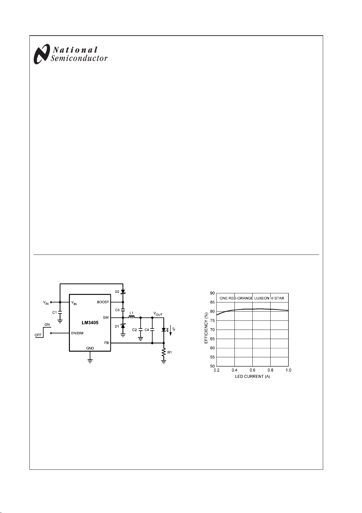
Typical Application Circuit
20178901
Efficiency vs LED Current (V
IN
= 5V)
20178971
© 2007 National Semiconductor Corporation 201789 www.national.com
LM3405 1.6MHz, 1A Constant Current Buck Regulator for Powering LEDs
Page 2
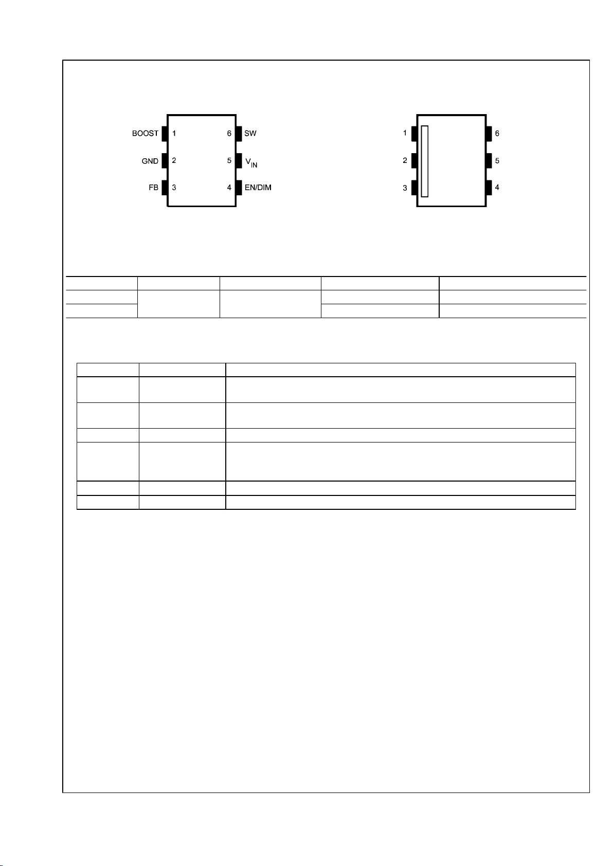
Connection Diagrams
20178905
6-Lead TSOT
NS Package Number MK06A
20178960
Pin 1 Identification
Ordering Information
Part Number Package Type NS Package Drawing Package Marking Supplied As
LM3405XMK
TSOT-6 MK06A
SPNB 1000 Units on Tape and Reel
LM3405XMKX SPNB 3000 Units on Tape and Reel
*NOPB versions are available
Pin Descriptions
Pin(s) Name Application Information
1 BOOST
Voltage at this pin drives the internal NMOS power switch. A bootstrap capacitor is
connected between the BOOST and SW pins.
2 GND
Signal and Power ground pin. Place the LED current-setting resistor as close as possible
to this pin for accurate current regulation.
3 FB Feedback pin. Connect an external resistor from FB to GND to set the LED Current.
4 EN/DIM
Enable control input. Logic high enables operation. Toggling this pin with a periodic logic
square wave of varying duty cycle at different frequencies controls the brightness of LEDs.
Do not allow this pin to float or be greater than VIN + 0.3V.
5 V
IN
Input supply voltage. Connect a bypass capacitor locally from this pin to GND.
6 SW Switch pin. Connect this pin to the inductor, catch diode, and bootstrap capacitor.
www.national.com 2
LM3405
Page 3
Absolute Maximum Ratings (Note 1)
If Military/Aerospace specified devices are required,
please contact the National Semiconductor Sales Office/
Distributors for availability and specifications.
V
IN
-0.5V to 20V
SW Voltage -0.5V to 20V
Boost Voltage -0.5V to 26V
Boost to SW Voltage -0.5V to 6.0V
FB Voltage -0.5V to 3.0V
EN/DIM Voltage
-0.5V to (VIN + 0.3V)
Junction Temperature 150°C
ESD Susceptibility (Note 2) 2kV
Storage Temperature -65°C to +150°C
Soldering Information
Infrared/Convection Reflow (15sec) 220°C
Operating Ratings (Note 1)
V
IN
3V to 15V
EN/DIM voltage
-0.5V to (VIN + 0.3V)
Boost to SW Voltage 2.5V to 5.5V
Junction Temperature Range -40°C to +125°C
Thermal Resistance θJA (Note 3)
118°C/W
Electrical Characteristics Unless otherwise specified, V
IN
= 12V. Limits in standard type are for TJ = 25°C only;
limits in boldface type apply over the junction temperature (TJ) range of -40°C to +125°C. Minimum and Maximum limits are
guaranteed through test, design, or statistical correlation. Typical values represent the most likely parametric norm, and are
provided for reference purposes only.
Symbol Parameter Conditions Min Typ Max Units
V
FB
Feedback Voltage 0.188 0.205 0.220 V
ΔVFB/(ΔVINxVFB)
Feedback Voltage Line Regulation
VIN = 3V to 15V
0.01
%/V
I
FB
Feedback Input Bias Current
Sink/Source 10 250
nA
UVLO
Under-voltage Lockout
VIN Rising 2.74 2.95
V
Under-voltage Lockout VIN Falling 1.9 2.3 V
UVLO Hysteresis 0.44 V
f
SW
Switching Frequency 1.2 1.6 1.9 MHz
D
MAX
Maximum Duty Cycle VFB = 0V 85 94 %
R
DS(ON)
Switch ON Resistance V
BOOST
- VSW = 3V 300 600
mΩ
I
CL
Switch Current Limit V
BOOST
- VSW = 3V, VIN = 3V 1.2 2.0 2.8 A
I
Q
Quiescent Current Switching, VFB = 0.195V 1.8 2.8 mA
Quiescent Current (Shutdown) V
EN/DIM
= 0V 0.3 µA
V
EN/DIM_TH
Enable Threshold Voltage
V
EN/DIM
Rising 1.8
V
Shutdown Threshold Voltage
V
EN/DIM
Falling 0.4
V
I
EN/DIM
EN/DIM Pin Current Sink/Source 0.01 µA
I
SW
Switch Leakage VIN = 15V 0.1
µA
Note 1: Absolute Maximum Ratings are limits beyond which damage to the device may occur. Operating Ratings define the conditions under which the device
is intended to be functional. For guaranteed specifications and test conditions, see the Electrical Characteristics.
Note 2: Human body model, 1.5kΩ in series with 100pF.
Note 3: Thermal shutdown will occur if the junction temperature (TJ) exceeds 165°C. The maximum allowable power dissipation (PD) at any ambient temperature
(TA) is PD = (T
J(MAX)
– TA)/θJA . This number applies to packages soldered directly onto a 3" x 3" PC board with 2oz. copper on 4 layers in still air. For a 2 layer
board using 1 oz. copper in still air, θJA = 204°C/W.
3 www.national.com
LM3405
Page 4
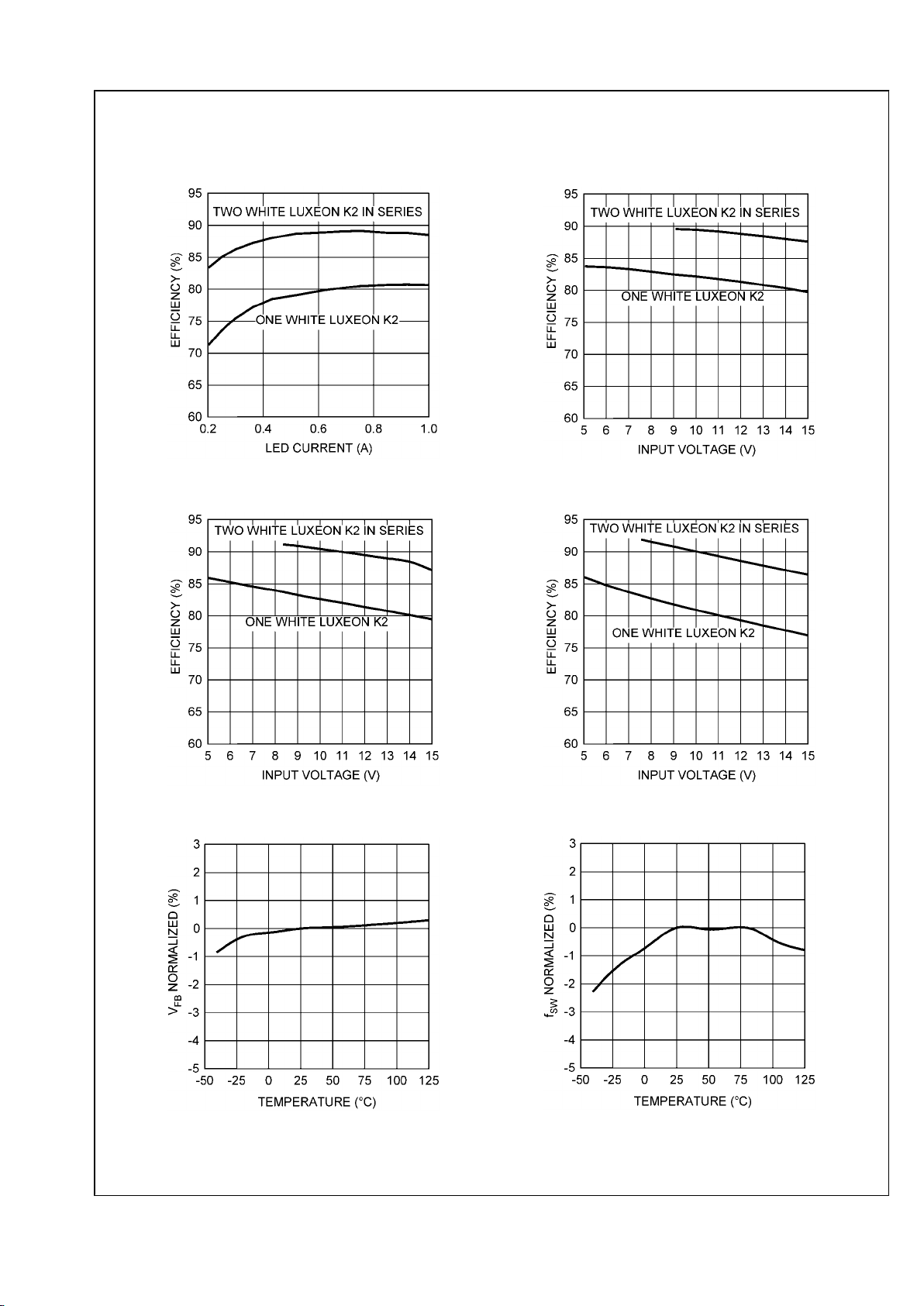
Typical Performance Characteristics Unless otherwise specified, V
IN
= 12V, V
BOOST
- VSW = 5V and
TA = 25°C.
Efficiency vs LED Current
20178973
Efficiency vs Input Voltage (IF = 1A)
20178931
Efficiency vs Input Voltage (IF = 0.7A)
20178932
Efficiency vs Input Voltage (IF = 0.35A)
20178933
VFB vs Temperature
20178927
Oscillator Frequency vs Temperature
20178936
www.national.com 4
LM3405
Page 5
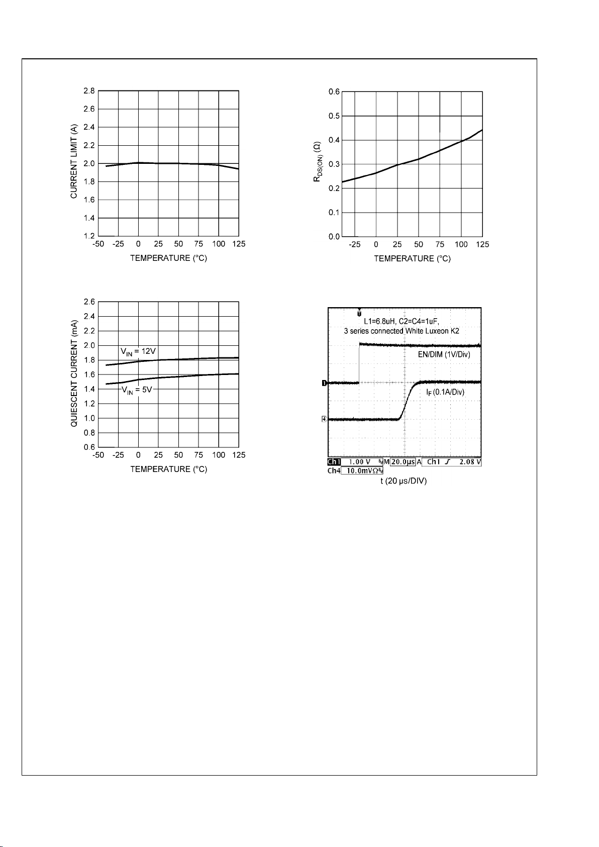
Current Limit vs Temperature
20178972
R
DS(ON)
vs Temperature (V
BOOST
- VSW = 3V)
20178930
Quiescent Current vs Temperature
20178934
Startup Response to EN/DIM Signal
(VIN = 15V, IF = 0.2A)
20178968
5 www.national.com
LM3405
Page 6
Block Diagram
20178906
FIGURE 1. Simplified Block Diagram
Application Information
THEORY OF OPERATION
The LM3405 is a PWM, current-mode control switching buck
regulator designed to provide a simple, high efficiency solution for driving LEDs with a preset switching frequency of
1.6MHz. This high frequency allows the LM3405 to operate
with small surface mount capacitors and inductors, resulting
in LED drivers that need only a minimum amount of board
space. The LM3405 is internally compensated, simple to use,
and requires few external components.
The following description of operation of the LM3405 will refer
to the Simplified Block Diagram (Figure 1) and to the waveforms in Figure 2. The LM3405 supplies a regulated output
current by switching the internal NMOS power switch at constant frequency and variable duty cycle. A switching cycle
begins at the falling edge of the reset pulse generated by the
internal oscillator. When this pulse goes low, the output control logic turns on the internal NMOS power switch. During this
on-time, the SW pin voltage (VSW) swings up to approximately
VIN, and the inductor current (IL) increases with a linear slope.
IL is measured by the current sense amplifier, which generates an output proportional to the switch current. The sense
signal is summed with the regulator’s corrective ramp and
compared to the error amplifier’s output, which is proportional
to the difference between the feedback voltage and V
REF
.
When the PWM comparator output goes high, the internal
power switch turns off until the next switching cycle begins.
During the switch off-time, inductor current discharges
through the catch diode D1, which forces the SW pin to swing
below ground by the forward voltage (VD1) of the catch diode.
The regulator loop adjusts the duty cycle (D) to maintain a
constant output current (IF) through the LED, by forcing FB
pin voltage to be equal to V
REF
(0.205V).
20178907
FIGURE 2. SW Pin Voltage and Inductor Current
Waveforms of LM3405
BOOST FUNCTION
Capacitor C3 and diode D2 in Figure 1 are used to generate
a voltage V
BOOST
. The voltage across C3, V
BOOST
- VSW, is
the gate drive voltage to the internal NMOS power switch. To
properly drive the internal NMOS switch during its on-time,
V
BOOST
needs to be at least 2.5V greater than VSW. Large
value of V
BOOST
- VSW is recommended to achieve better efficiency by minimizing both the internal switch ON resistance
(R
DS(ON)
), and the switch rise and fall times. However,
V
BOOST
- VSW should not exceed the maximum operating limit
of 5.5V.
www.national.com 6
LM3405
Page 7

When the LM3405 starts up, internal circuitry from VIN supplies a 20mA current to the BOOST pin, flowing out of the
BOOST pin into C3. This current charges C3 to a voltage sufficient to turn the switch on. The BOOST pin will continue to
source current to C3 until the voltage at the feedback pin is
greater than 123mV.
There are various methods to derive V
BOOST
:
1.
From the input voltage (VIN)
2.
From the output voltage (V
OUT
)
3.
From a shunt or series zener diode
4.
From an external distributed voltage rail (V
EXT
)
The first method is shown in the Simplified Block Diagram of
Figure 1. Capacitor C3 is charged via diode D2 by VIN. During
a normal switching cycle, when the internal NMOS power
switch is off (T
OFF
) (refer to Figure 2), V
BOOST
equals VIN minus the forward voltage of D2 (VD2), during which the current
in the inductor (L1) forward biases the catch diode D1 (VD1).
Therefore the gate drive voltage stored across C3 is:
V
BOOST
- VSW = VIN - VD2 + V
D1
When the NMOS switch turns on (TON), the switch pin rises
to:
VSW = VIN – (R
DS(ON)
x IL)
Since the voltage across C3 remains unchanged, V
BOOST
is
forced to rise thus reverse biasing D2. The voltage at
V
BOOST
is then:
V
BOOST
= 2VIN – (R
DS(ON)
x IL) – VD2 + V
D1
Depending on the quality of the diodes D1 and D2, the gate
drive voltage in this method can be slightly less or larger than
the input voltage VIN. For best performance, ensure that the
variation of the input supply does not cause the gate drive
voltage to fall outside the recommended range:
2.5V < VIN - VD2 + VD1 < 5.5V
The second method for deriving the boost voltage is to connect D2 to the output as shown in Figure 3. The gate drive
voltage in this configuration is:
V
BOOST
- VSW = V
OUT
– VD2 + V
D1
Since the gate drive voltage needs to be in the range of 2.5V
to 5.5V, the output voltage V
OUT
should be limited to a certain
range. For the calculation of V
OUT
, see OUTPUT VOLTAGE
section.
20178993
FIGURE 3. V
BOOST
derived from V
OUT
The third method can be used in the applications where both
VIN and V
OUT
are greater than 5.5V. In these cases, C3 cannot
be charged directly from these voltages; instead C3 can be
charged from VIN or V
OUT
minus a zener voltage (VD3) by
placing a zener diode D3 in series with D2 as shown in Figure
4. When using a series zener diode from the input, the gate
drive voltage is VIN - VD3 - VD2 + VD1.
20178999
FIGURE 4. V
BOOST
derived from VIN through a Series
Zener
An alternate method is to place the zener diode D3 in a shunt
configuration as shown in Figure 5. A small 350mW to
500mW, 5.1V zener in a SOT-23 or SOD package can be
used for this purpose. A small ceramic capacitor such as a
6.3V, 0.1µF capacitor (C5) should be placed in parallel with
the zener diode. When the internal NMOS switch turns on, a
pulse of current is drawn to charge the internal NMOS gate
capacitance. The 0.1µF parallel shunt capacitor ensures that
the V
BOOST
voltage is maintained during this time. Resistor R2
should be chosen to provide enough RMS current to the zener
diode and to the BOOST pin. A recommended choice for the
zener current (I
ZENER
) is 1mA. The current I
BOOST
into the
BOOST pin supplies the gate current of the NMOS power
switch. It reaches a maximum of around 3.6mA at the highest
gate drive voltage of 5.5V over the LM3405 operating range.
For the worst case I
BOOST
, increase the current by 50%. In
that case, the maximum boost current will be:
I
BOOST-MAX
= 1.5 x 3.6mA = 5.4mA
R2 will then be given by:
R2 = (VIN - V
ZENER
) / (I
BOOST_MAX
+ I
ZENER
)
For example, let VIN = 12V, V
ZENER
= 5V, I
ZENER
= 1mA, then:
R2 = (12V - 5V) / (5.4mA + 1mA) = 1.09kΩ
20178994
FIGURE 5. V
BOOST
derived from VIN through a Shunt Zener
7 www.national.com
LM3405
Page 8

The fourth method can be used in an application which has
an external low voltage rail, V
EXT
. C3 can be charged through
D2 from V
EXT
, independent of VIN and V
OUT
voltage levels.
Again for best performance, ensure that the gate drive voltage, V
EXT
- VD2 + VD1, falls in the range of 2.5V to 5.5V.
SETTING THE LED CURRENT
LM3405 is a constant current buck regulator. The LEDs are
connected between V
OUT
and FB pin as shown in the Typical
Application Circuit. The FB pin is at 0.205V in regulation and
therefore the LED current IF is set by VFB and the resistor R1
from FB to ground by the following equation:
IF = VFB / R1
IF should not exceed the 1A current capability of LM3405 and
therefore R1 minimum must be approximately 0.2Ω. IF should
also be kept above 200mA for stable operation, and therefore
R1 maximum must be approximately 1Ω. If average LED currents less than 200mA are desired, the EN/DIM pin can be
used for PWM dimming. See LED PWM DIMMING section.
OUTPUT VOLTAGE
The output voltage is primarily determined by the number of
LEDs (n) connected from V
OUT
to FB pin and therefore V
OUT
can be written as :
V
OUT
= ((n x VF) + VFB)
where VF is the forward voltage of one LED at the set LED
current level (see LED manufacturer datasheet for forward
characteristics curve).
ENABLE MODE / SHUTDOWN MODE
The LM3405 has both enable and shutdown modes that are
controlled by the EN/DIM pin. Connecting a voltage source
greater than 1.8V to the EN/DIM pin enables the operation of
LM3405, while reducing this voltage below 0.4V places the
part in a low quiescent current (0.3µA typical) shutdown
mode. There is no internal pull-up on EN/DIM pin, therefore
an external signal is required to initiate switching. Do not allow
this pin to float or rise to 0.3V above VIN. It should be noted
that when the EN/DIM pin voltage rises above 1.8V while the
input voltage is greater than UVLO, there is a finite delay before switching starts. During this delay the LM3405 will go
through a power on reset state after which the internal softstart process commences. The soft-start process limits the
inrush current and brings up the LED current (IF) in a smooth
and controlled fashion. The total combined duration of the
power on reset delay, soft-start delay and the delay to fully
establish the LED current is in the order of 100µs (refer to
Figure 11).
The simplest way to enable the operation of LM3405 is to
connect the EN/DIM pin to VIN which allows self start-up of
LM3405 whenever the input voltage is applied. However,
when an input voltage of slow rise time is used to power the
application and if both the input voltage and the output voltage
are not fully established before the soft-start time elapses, the
control circuit will command maximum duty cycle operation of
the internal power switch to bring up the output voltage rapidly. When the feedback pin voltage exceeds 0.205V, the duty
cycle will have to reduce from the maximum value accordingly, to maintain regulation. It takes a finite amount of time for
this reduction of duty cycle and this will result in a spike in LED
current for a short duration as shown in Figure 6. In applications where this LED current overshoot is undesirable, EN/
DIM pin voltage can be delayed with respect to VIN such that
VIN is fully established before the EN/DIM pin voltage reaches
the enable threshold. This delay can be implemented by a
simple Ra-Ca network as shown in Figure 7. The effect of
adding this Ra-Ca network on the LED current is shown in
Figure 8. For a fast rising input voltage (200µs for example),
there is no need to delay the EN/DIM signal since soft-start
can smoothly bring up the LED current as shown in Figure
9.
20178976
FIGURE 6. Startup Response to VIN with 5ms rise time
20178998
FIGURE 7. EN/DIM delayed with respect to V
IN
20178977
FIGURE 8. Startup Response to VIN with EN/DIM delayed
www.national.com 8
LM3405
Page 9

20178975
FIGURE 9. Startup Response to VIN with 200µs rise time
LED PWM DIMMING
The LED brightness can be controlled by applying a periodic
pulse signal to the EN/DIM pin and varying its frequency and/
or duty cycle. This so-called PWM dimming method controls
the average light output by pulsing the LED current between
the set value and zero. A logic high level at the EN/DIM pin
turns on the LED current whereas a logic low level turns off
the LED current. Figure 10 shows a typical LED current waveform in PWM dimming mode. As explained in the previous
section, there is approximately a 100µs delay from the EN/
DIM signal going high to fully establishing the LED current as
shown in Figure 11. This 100µs delay sets a maximum frequency limit for the driving signal that can be applied to the
EN/DIM pin for PWM dimming. Figure 12 shows the average
LED current versus duty cycle of PWM dimming signal for
various frequencies. The applicable frequency range to drive
LM3405 for PWM dimming is from 100Hz to 5kHz. The dimming ratio reduces drastically when the applied PWM dimming frequency is greater than 5kHz.
20178966
FIGURE 10. PWM Dimming of LEDs using the EN/DIM Pin
20178967
FIGURE 11. Startup Response to EN/DIM with IF = 1A
20178983
FIGURE 12. Average LED Current versus Duty Cycle of
PWM Dimming Signal at EN/DIM Pin
UNDER-VOLTAGE LOCKOUT
Under-voltage lockout (UVLO) prevents the LM3405 from operating until the input voltage exceeds 2.74V (typical). The
UVLO threshold has approximately 440mV of hysteresis, so
the part will operate until VIN drops below 2.3V (typical). Hysteresis prevents the part from turning off during power up if
VIN is non-monotonic.
CURRENT LIMIT
The LM3405 uses cycle-by-cycle current limit to protect the
internal power switch. During each switching cycle, a current
limit comparator detects if the power switch current exceeds
2.0A (typical), and turns off the switch until the next switching
cycle begins.
OVER-CURRENT PROTECTION
The LM3405 has a built in over-current comparator that compares the FB pin voltage to a threshold voltage that is 60%
higher than the internal reference V
REF
. Once the FB pin voltage exceeds this threshold level (typically 328mV), the internal NMOS power switch is turned off, which allows the
feedback voltage to decrease towards regulation. This
9 www.national.com
LM3405
Page 10

threshold provides an upper limit for the LED current. LED
current overshoot is limited to 328mV/R1 by this comparator
during transients.
THERMAL SHUTDOWN
Thermal shutdown limits total power dissipation by turning off
the internal power switch when the IC junction temperature
exceeds 165°C. After thermal shutdown occurs, the power
switch does not turn on until the junction temperature drops
below approximately 150°C.
Design Guide
INDUCTOR (L1)
The Duty Cycle (D) can be approximated quickly using the
ratio of output voltage (V
OUT
) to input voltage (VIN):
The catch diode (D1) forward voltage drop and the voltage
drop across the internal NMOS must be included to calculate
a more accurate duty cycle. Calculate D by using the following
formula:
VSW can be approximated by:
VSW = IF x R
DS(ON)
The diode forward drop (VD1) can range from 0.3V to 0.7V
depending on the quality of the diode. The lower VD1 is, the
higher the operating efficiency of the converter.
The inductor value determines the output ripple current (ΔiL,
as defined in Figure 2). Lower inductor values decrease the
size of the inductor, but increases the output ripple current.
An increase in the inductor value will decrease the output ripple current. The ratio of ripple current to LED current is
optimized when it is set between 0.3 and 0.4 at 1A LED current. This ratio r is defined as:
One must also ensure that the minimum current limit (1.2A)
is not exceeded, so the peak current in the inductor must be
calculated. The peak current (I
LPK
) in the inductor is calculated
as:
I
LPK
= IF + ΔiL/2
When the designed maximum output current is reduced, the
ratio r can be increased. At a current of 0.2A, r can be made
as high as 0.7. The ripple ratio can be increased at lighter
loads because the net ripple is actually quite low, and if r remains constant the inductor value can be made quite large.
An equation empirically developed for the maximum ripple
ratio at any current below 2A is:
r = 0.387 x I
OUT
-0.3667
Note that this is just a guideline.
The LM3405 operates at a high frequency allowing the use of
ceramic output capacitors without compromising transient re-
sponse. Ceramic capacitors allow higher inductor ripple without significantly increasing LED current ripple. See the output
capacitor and feed-forward capacitor sections for more details on LED current ripple.
Now that the ripple current or ripple ratio is determined, the
inductance is calculated by:
where fSW is the switching frequency and IF is the LED current.
When selecting an inductor, make sure that it is capable of
supporting the peak output current without saturating. Inductor saturation will result in a sudden reduction in inductance
and prevent the regulator from operating correctly. Because
of the operating frequency of LM3405, ferrite based inductors
are preferred to minimize core losses. This presents little restriction since the variety of ferrite based inductors is huge.
Lastly, inductors with lower series resistance (DCR) will provide better operating efficiency. For recommended inductor
selection, refer to Circuit Examples and Recommended Inductance Range in Table 1. Note that it is a good practice to
use small inductance value at light load (for example, IF =
0.2A) to increase inductor current ramp signal, such that noise
immunity is improved.
TABLE 1. Recommended Inductance Range
IFInductance Range and Inductor Current Ripple
1.0A
4.7µH-10µH
Inductance 4.7µH 6.8µH 10µH
ΔiL / IF*
51% 35% 24%
0.6A
6.8µH-15µH
Inductance 6.8µH 10µH 15µH
ΔiL / IF*
58% 40% 26%
0.2A
4.7µH**-22µH
Inductance 10µH 15µH 22µH
ΔiL / IF*
119% 79% 54%
*Maximum over full range of VIN and V
OUT
.
**Small inductance improves stability without causing a significant increase
in LED current ripple.
INPUT CAPACITOR (C1)
An input capacitor is necessary to ensure that VIN does not
drop excessively during switching transients. The primary
specifications of the input capacitor are capacitance, voltage
rating, RMS current rating, and ESL (Equivalent Series Inductance). The input voltage rating is specifically stated by
the capacitor manufacturer. Make sure to check any recommended deratings and also verify if there is any significant
change in capacitance at the operating input voltage and the
operating temperature. The input capacitor maximum RMS
input current rating (I
RMS-IN
) must be greater than:
It can be shown from the above equation that maximum RMS
capacitor current occurs when D = 0.5. Always calculate the
RMS at the point where the duty cycle D, is closest to 0.5. The
ESL of an input capacitor is usually determined by the effective cross sectional area of the current path. A large leaded
www.national.com 10
LM3405
Page 11

capacitor will have high ESL and a 0805 ceramic chip capacitor will have very low ESL. At the operating frequency of the
LM3405, certain capacitors may have an ESL so large that
the resulting inductive impedance (2πfL) will be higher than
that required to provide stable operation. It is strongly recommended to use ceramic capacitors due to their low ESR and
low ESL. A 10µF multilayer ceramic capacitor (MLCC) is a
good choice for most applications. In cases where large capacitance is required, use surface mount capacitors such as
Tantalum capacitors and place at least a 1µF ceramic capacitor close to the VIN pin. For MLCCs it is recommended to use
X7R or X5R dielectrics. Consult capacitor manufacturer
datasheet to see how rated capacitance varies over operating
conditions.
OUTPUT CAPACITOR (C2)
The output capacitor is selected based upon the desired reduction in LED current ripple. A 1µF ceramic capacitor results
in very low LED current ripple for most applications. Due to
the high switching frequency, the 1µF capacitor alone (without
feed-forward capacitor C4) can filter more than 90% of the
inductor current ripple for most applications where the sum of
LED dynamic resistance and R1 is larger than 1Ω. Since the
internal compensation is tailored for small output capacitance
with very low ESR, it is strongly recommended to use a ceramic capacitor with capacitance less than 3.3µF.
Given the availability and quality of MLCCs and the expected
output voltage of designs using the LM3405, there is really no
need to review other capacitor technologies. A benefit of ceramic capacitors is their ability to bypass high frequency
noise. A certain amount of switching edge noise will couple
through the parasitic capacitances in the inductor to the output. A ceramic capacitor will bypass this noise. In cases where
large capacitance is required, use Electrolytic or Tantalum
capacitors with large ESR, and verify the loop performance
on bench. Like the input capacitor, recommended multilayer
ceramic capacitors are X7R or X5R. Again, verify actual capacitance at the desired operating voltage and temperature.
Check the RMS current rating of the capacitor. The maximum
RMS current rating of the capacitor is:
One may select a 1206 size ceramic capacitor for C2, since
its current rating is typically higher than 1A, more than enough
for the requirement.
FEED-FORWARD CAPACITOR (C4)
The feed-forward capacitor (designated as C4) connected in
parallel with the LED string is required to provide multiple
benefits to the LED driver design. It greatly improves the large
signal transient response and suppresses LED current overshoot that may otherwise occur during PWM dimming; it also
helps to shape the rise and fall times of the LED current pulse
during PWM dimming thus reducing EMI emission; it reduces
LED current ripple by bypassing some of inductor ripple from
flowing through the LED. For most applications, a 1µF ceramic capacitor is sufficient. In fact, the combination of a 1µF
feed-forward ceramic capacitor and a 1µF output ceramic capacitor leads to less than 1% current ripple flowing through
the LED. Lower and higher C4 values can be used, but bench
validation is required to ensure the performance meets the
application requirement.
Figure 13 shows a typical LED current waveform during PWM
dimming without feed-forward capacitor. At the beginning of
each PWM cycle, overshoot can be seen in the LED current.
Adding a 1µF feed-forward capacitor can totally remove the
overshoot as shown in Figure 14.
20178969
FIGURE 13. PWM Dimming without Feed-Forward
Capacitor
20178970
FIGURE 14. PWM Dimming with a 1µF Feed-Forward
Capacitor
CATCH DIODE (D1)
The catch diode (D1) conducts during the switch off-time. A
Schottky diode is required for its fast switching time and low
forward voltage drop. The catch diode should be chosen such
that its current rating is greater than:
ID1 = IF x (1-D)
The reverse breakdown rating of the diode must be at least
the maximum input voltage plus appropriate margin. To improve efficiency, choose a Schottky diode with a low forward
voltage drop.
BOOST DIODE (D2)
A standard diode such as the 1N4148 type is recommended.
For V
BOOST
circuits derived from voltages less than 3.3V, a
small-signal Schottky diode is recommended for better efficiency. A good choice is the BAT54 small signal diode.
11 www.national.com
LM3405
Page 12

BOOST CAPACITOR (C3)
A 0.01µF ceramic capacitor with a voltage rating of at least
6.3V is sufficient. The X7R and X5R MLCCs provide the best
performance.
POWER LOSS ESTIMATION
The main power loss in LM3405 includes three basic types of
loss in the internal power switch: conduction loss, switching
loss, and gate charge loss. In addition, there is loss associated with the power required for the internal circuitry of IC.
The conduction loss is calculated as:
If the inductor ripple current is fairly small (for example, less
than 40%) , the conduction loss can be simplified to:
P
COND
= I
F
2
x R
DS(ON)
x D
The switching loss occurs during the switch on and off transition periods, where voltage and current overlap resulting in
power loss. The simplest means to determine this loss is to
empirically measure the rise and fall times (10% to 90%) of
the voltage at the switch pin.
Switching power loss is calculated as follows:
PSW = 0.5 x VIN x IF x fSW x ( T
RISE
+ T
FALL
)
The gate charge loss is associated with the gate charge Q
G
required to drive the switch:
PG = fSW x VIN x Q
G
The power loss required for operation of the internal circuitry:
PQ = IQ x V
IN
IQ is the quiescent operating current, and is typically around
1.8mA for the LM3405.
The total power loss in the IC is:
P
INTERNAL
= P
COND
+ PSW + PG + P
Q
An example of power losses for a typical application is shown
in Table 2:
TABLE 2. Power Loss Tabulation
Conditions Power loss
V
IN
12V
V
OUT
4.1V
I
OUT
1.0A
V
D1
0.45V
R
DS(ON)
300mΩ
P
COND
111mW
f
SW
1.6MHz
T
RISE
18ns
P
SW
288mW
T
FALL
12ns
I
Q
1.8mA P
Q
22mW
Q
G
1.4nC P
G
27mW
D is calculated to be 0.37
Σ ( P
COND
+ PSW + PQ + PG ) = P
INTERNAL
P
INTERNAL
= 448mW
PCB Layout Considerations
When planning layout there are a few things to consider when
trying to achieve a clean, regulated output. The most important consideration when completing the layout is the close
coupling of the GND connections of the input capacitor C1
and the catch diode D1. These ground ends should be close
to one another and be connected to the GND plane with at
least two through-holes. Place these components as close to
the IC as possible. The next consideration is the location of
the GND connection of the output capacitor C2, which should
be near the GND connections of C1 and D1.
There should be a continuous ground plane on the bottom
layer of a two-layer board except under the switching node
island.
The FB pin is a high impedance node and care should be
taken to make the FB trace short to avoid noise pickup that
causes inaccurate regulation. The LED current setting resistor R1 should be placed as close as possible to the IC, with
the GND of R1 placed as close as possible to the GND of the
IC. The V
OUT
trace to LED anode should be routed away from
the inductor and any other traces that are switching.
High AC currents flow through the VIN, SW and V
OUT
traces,
so they should be as short and wide as possible. Radiated
noise can be decreased by choosing a shielded inductor.
The remaining components should also be placed as close
as possible to the IC. Please see Application Note AN-1229
for further considerations and the LM3405 demo board as an
example of a four-layer layout.
www.national.com 12
LM3405
Page 13

LM3405 Circuit Examples
20178942
FIGURE 15. V
BOOST
derived from V
IN
( VIN = 5V, IF = 1A )
Bill of Materials for Figure 15
Part ID Part Value Part Number Manufacturer
U1 1A LED Driver LM3405 National Semiconductor
C1, Input Cap 10µF, 6.3V, X5R C3216X5R0J106M TDK
C2, Output Cap 1µF, 10V, X7R GRM319R71A105KC01D Murata
C3, Boost Cap 0.01µF, 16V, X7R 0805YC103KAT2A AVX
C4, Feedforward Cap 1µF, 10V, X7R GRM319R71A105KC01D Murata
D1, Catch Diode Schottky, 0.37V at 1A, VR = 10V MBRM110LT1G ON Semiconductor
D2, Boost Diode Schottky, 0.36V at 15mA CMDSH-3 Central Semiconductor
L1 4.7µH, 1.6A SLF6028T-4R7M1R6 TDK
R1
0.2Ω, 0.5W, 1%
WSL2010R2000FEA Vishay
LED1 1A, White LED LXHL-PW09 Lumileds
13 www.national.com
LM3405
Page 14

20178943
FIGURE 16. V
BOOST
derived from V
OUT
( VIN = 12V, IF = 1A )
Bill of Materials for Figure 16
Part ID Part Value Part Number Manufacturer
U1 1A LED Driver LM3405 National Semiconductor
C1, Input Cap 10µF, 25V, X5R ECJ-3YB1E106K Panasonic
C2, Output Cap 1µF, 10V, X7R GRM319R71A105KC01D Murata
C3, Boost Cap 0.01µF, 16V, X7R 0805YC103KAT2A AVX
C4, Feedforward Cap 1µF, 10V, X7R GRM319R71A105KC01D Murata
D1, Catch Diode Schottky, 0.5V at 1A, VR = 30V SS13 Vishay
D2, Boost Diode Schottky, 0.36V at 15mA CMDSH-3 Central Semiconductor
L1 4.7µH, 1.6A SLF6028T-4R7M1R6 TDK
R1
0.2Ω, 0.5W, 1%
WSL2010R2000FEA Vishay
LED1 1A, White LED LXHL-PW09 Lumileds
www.national.com 14
LM3405
Page 15

20178944
FIGURE 17. V
BOOST
derived from VIN through a Shunt Zener Diode (D3)
( VIN = 15V, IF = 1A )
Bill of Materials for Figure 17
Part ID Part Value Part Number Manufacturer
U1 1A LED Driver LM3405 National Semiconductor
C1, Input Cap 10µF, 25V, X5R ECJ-3YB1E106K Panasonic
C2, Output Cap 1µF, 10V, X7R GRM319R71A105KC01D Murata
C3, Boost Cap 0.01µF, 16V, X7R 0805YC103KAT2A AVX
C4, Feedforward Cap 1µF, 10V, X7R GRM319R71A105KC01D Murata
C5, Shunt Cap 0.1µF, 16V, X7R GRM219R71C104KA01D Murata
D1, Catch Diode Schottky, 0.5V at 1A, VR = 30V SS13 Vishay
D2, Boost Diode Schottky, 0.36V at 15mA CMDSH-3 Central Semiconductor
D3, Zener Diode 4.7V, 350mW, SOT-23 BZX84C4V7 Fairchild
L1 6.8µH, 1.5A SLF6028T-6R8M1R5 TDK
R1
0.2Ω, 0.5W, 1%
WSL2010R2000FEA Vishay
R2
1.91kΩ, 1%
CRCW08051K91FKEA Vishay
LED1 1A, White LED LXHL-PW09 Lumileds
15 www.national.com
LM3405
Page 16

20178949
FIGURE 18. V
BOOST
derived from VIN through a Series Zener Diode (D3)
( VIN = 15V, IF = 1A )
Bill of Materials for Figure 18
Part ID Part Value Part Number Manufacturer
U1 1A LED Driver LM3405 National Semiconductor
C1, Input Cap 10µF, 25V, X5R ECJ-3YB1E106K Panasonic
C2, Output Cap 1µF, 10V, X7R GRM319R71A105KC01D Murata
C3, Boost Cap 0.01µF, 16V, X7R 0805YC103KAT2A AVX
C4, Feedforward Cap 1µF, 10V, X7R GRM319R71A105KC01D Murata
D1, Catch Diode Schottky, 0.5V at 1A, VR = 30V SS13 Vishay
D2, Boost Diode Schottky, 0.36V at 15mA CMDSH-3 Central Semiconductor
D3, Zener Diode 11V, 350mW, SOT-23 BZX84C11 Fairchild
L1 6.8µH, 1.5A SLF6028T-6R8M1R5 TDK
R1
0.2Ω, 0.5W, 1%
WSL2010R2000FEA Vishay
LED1 1A, White LED LXHL-PW09 Lumileds
www.national.com 16
LM3405
Page 17

20178950
FIGURE 19. V
BOOST
derived from V
OUT
through a Series Zener Diode (D3)
( VIN = 15V, IF = 1A )
Bill of Materials for Figure 19
Part ID Part Value Part Number Manufacturer
U1 1A LED Driver LM3405 National Semiconductor
C1, Input Cap 10µF, 25V, X5R ECJ-3YB1E106K Panasonic
C2, Output Cap 1µF, 16V, X7R GRM319R71A105KC01D Murata
C3, Boost Cap 0.01µF, 16V, X7R 0805YC103KAT2A AVX
C4, Feedforward Cap 1µF, 16V, X7R GRM319R71A105KC01D Murata
D1, Catch Diode Schottky, 0.5V at 1A, VR = 30V SS13 Vishay
D2, Boost Diode Schottky, 0.36V at 15mA CMDSH-3 Central Semiconductor
D3, Zener Diode 3.9V, 350mW, SOT-23 BZX84C3V9 Fairchild
L1 6.8µH, 1.5A SLF6028T-6R8M1R5 TDK
R1
0.2Ω, 0.5W, 1%
WSL2010R2000FEA Vishay
LED1 1A, White LED LXHL-PW09 Lumileds
LED2 1A, White LED LXHL-PW09 Lumileds
17 www.national.com
LM3405
Page 18

Physical Dimensions inches (millimeters) unless otherwise noted
6-Lead TSOT Package
NS Package Number MK06A
www.national.com 18
LM3405
Page 19

Notes
19 www.national.com
LM3405
Page 20

Notes
LM3405 1.6MHz, 1A Constant Current Buck Regulator for Powering LEDs
THE CONTENTS OF THIS DOCUMENT ARE PROVIDED IN CONNECTION WITH NATIONAL SEMICONDUCTOR CORPORATION
(“NATIONAL”) PRODUCTS. NATIONAL MAKES NO REPRESENTATIONS OR WARRANTIES WITH RESPECT TO THE ACCURACY
OR COMPLETENESS OF THE CONTENTS OF THIS PUBLICATION AND RESERVES THE RIGHT TO MAKE CHANGES TO
SPECIFICATIONS AND PRODUCT DESCRIPTIONS AT ANY TIME WITHOUT NOTICE. NO LICENSE, WHETHER EXPRESS,
IMPLIED, ARISING BY ESTOPPEL OR OTHERWISE, TO ANY INTELLECTUAL PROPERTY RIGHTS IS GRANTED BY THIS
DOCUMENT.
TESTING AND OTHER QUALITY CONTROLS ARE USED TO THE EXTENT NATIONAL DEEMS NECESSARY TO SUPPORT
NATIONAL’S PRODUCT WARRANTY. EXCEPT WHERE MANDATED BY GOVERNMENT REQUIREMENTS, TESTING OF ALL
PARAMETERS OF EACH PRODUCT IS NOT NECESSARILY PERFORMED. NATIONAL ASSUMES NO LIABILITY FOR
APPLICATIONS ASSISTANCE OR BUYER PRODUCT DESIGN. BUYERS ARE RESPONSIBLE FOR THEIR PRODUCTS AND
APPLICATIONS USING NATIONAL COMPONENTS. PRIOR TO USING OR DISTRIBUTING ANY PRODUCTS THAT INCLUDE
NATIONAL COMPONENTS, BUYERS SHOULD PROVIDE ADEQUATE DESIGN, TESTING AND OPERATING SAFEGUARDS.
EXCEPT AS PROVIDED IN NATIONAL’S TERMS AND CONDITIONS OF SALE FOR SUCH PRODUCTS, NATIONAL ASSUMES NO
LIABILITY WHATSOEVER, AND NATIONAL DISCLAIMS ANY EXPRESS OR IMPLIED WARRANTY RELATING TO THE SALE
AND/OR USE OF NATIONAL PRODUCTS INCLUDING LIABILITY OR WARRANTIES RELATING TO FITNESS FOR A PARTICULAR
PURPOSE, MERCHANTABILITY, OR INFRINGEMENT OF ANY PATENT, COPYRIGHT OR OTHER INTELLECTUAL PROPERTY
RIGHT.
LIFE SUPPORT POLICY
NATIONAL’S PRODUCTS ARE NOT AUTHORIZED FOR USE AS CRITICAL COMPONENTS IN LIFE SUPPORT DEVICES OR
SYSTEMS WITHOUT THE EXPRESS PRIOR WRITTEN APPROVAL OF THE CHIEF EXECUTIVE OFFICER AND GENERAL
COUNSEL OF NATIONAL SEMICONDUCTOR CORPORATION. As used herein:
Life support devices or systems are devices which (a) are intended for surgical implant into the body, or (b) support or sustain life and
whose failure to perform when properly used in accordance with instructions for use provided in the labeling can be reasonably expected
to result in a significant injury to the user. A critical component is any component in a life support device or system whose failure to perform
can be reasonably expected to cause the failure of the life support device or system or to affect its safety or effectiveness.
National Semiconductor and the National Semiconductor logo are registered trademarks of National Semiconductor Corporation. All other
brand or product names may be trademarks or registered trademarks of their respective holders.
Copyright© 2007 National Semiconductor Corporation
For the most current product information visit us at www.national.com
National Semiconductor
Americas Customer
Support Center
Email:
new.feedback@nsc.com
Tel: 1-800-272-9959
National Semiconductor Europe
Customer Support Center
Fax: +49 (0) 180-530-85-86
Email: europe.support@nsc.com
Deutsch Tel: +49 (0) 69 9508 6208
English Tel: +49 (0) 870 24 0 2171
Français Tel: +33 (0) 1 41 91 8790
National Semiconductor Asia
Pacific Customer Support Center
Email: ap.support@nsc.com
National Semiconductor Japan
Customer Support Center
Fax: 81-3-5639-7507
Email: jpn.feedback@nsc.com
Tel: 81-3-5639-7560
www.national.com
 Loading...