

Page 1
June 2007
LM3404/04HV
1.0A Constant Current Buck Regulator for Driving High
Power LEDs
General Description
The LM3404/04HV are monolithic switching regulators designed to deliver constant currents to high power LEDs. Ideal
for automotive, industrial, and general lighting applications,
they contain a high-side N-channel MOSFET switch with a
current limit of 1.5A (typical) for step-down (Buck) regulators.
Hysteretic controlled on-time and an external resistor allow
the converter output voltage to adjust as needed to deliver a
constant current to series and series-parallel connected LED
arrays of varying number and type. LED dimming via pulse
width modulation (PWM), broken/open LED protection, lowpower shutdown and thermal shutdown complete the feature
set.
Features
■
Integrated 1.0A MOSFET
■
VIN Range 6V to 42V (LM3404)
■
VIN Range 6V to 75V (LM3404HV)
■
1.2A Output Current Over Temperature
■
Cycle-by-Cycle Current Limit
■
No Control Loop Compensation Required
■
Separate PWM Dimming and Low Power Shutdown
■
Supports all-ceramic output capacitors and capacitor-less
outputs
■
Thermal shutdown protection
■
SO-8 Package, PSOP-8 Package
Applications
■
LED Driver
■
Constant Current Source
■
Automotive Lighting
■
General Illumination
■
Industrial Lighting
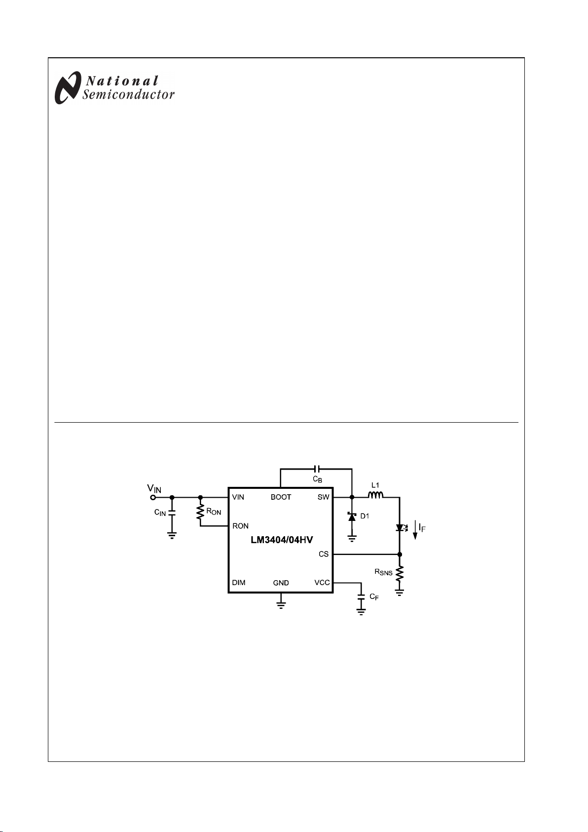
Typical Application
20205401
© 2007 National Semiconductor Corporation 202054 www.national.com
LM3404/04HV 1.0A Constant Current Buck Regulator for Driving High Power LEDs
Page 2
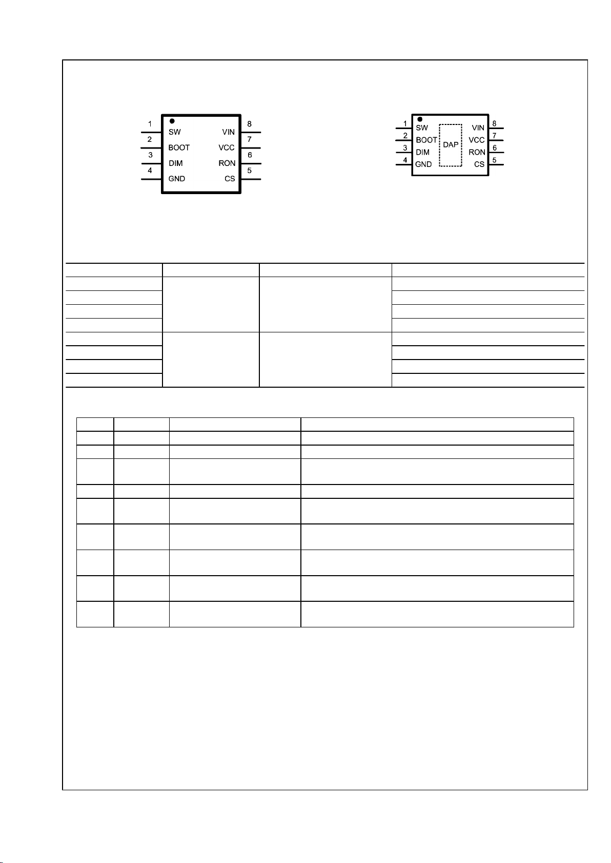
Connection Diagrams
20205402
8-Lead Plastic SO-8 Package
NS Package Number M08A
20205456
8-Lead Plastic PSOP-8 Package
NS Package Number MRA08B
Ordering Information
Order Number Package Type NSC Package Drawing Supplied As
LM3404MA
SO-8 M08A
95 units in anti-static rails
LM3404MAX 2500 units on tape and reel
LM3404HVMA 95 units in anti-static rails
LM3404HVMAX 2500 units on tape and reel
LM3404MR
PSOP-8 MRA08B
95 units in anti-static rails
LM3404MRX 2500 units on tape and reel
LM3404HVMR 95 units in anti-static rails
LM3404HVMRX 2500 units on tape and reel
Pin Descriptions
Pin(s) Name Description Application Information
1 SW Switch pin Connect this pin to the output inductor and Schottky diode.
2 BOOT MOSFET drive bootstrap pin Connect a 10 nF ceramic capacitor from this pin to SW.
3 DIM Input for PWM dimming Connect a logic-level PWM signal to this pin to enable/disable the
power MOSFET and reduce the average light output of the LED array.
4 GND Ground pin Connect this pin to system ground.
5 CS Current sense feedback pin Set the current through the LED array by connecting a resistor from
this pin to ground.
6 RON On-time control pin A resistor connected from this pin to VIN sets the regulator controlled
on-time.
7 VCC Output of the internal 7V linear
regulator
Bypass this pin to ground with a minimum 0.1 µF ceramic capacitor
with X5R or X7R dielectric.
8 VIN Input voltage pin Nominal operating input range for this pin is 6V to 42V (LM3404) or 6V
to 75V (LM3404HV).
DAP GND Thermal Pad Connect to ground. Place 4-6 vias from DAP to bottom layer ground
plane.
www.national.com 2
LM3404/LM3404HV
Page 3

Absolute Maximum Ratings
(LM3404) (Note 1)
If Military/Aerospace specified devices are required,
please contact the National Semiconductor Sales Office/
Distributors for availability and specifications.
VIN to GND -0.3V to 45V
BOOT to GND -0.3V to 59V
SW to GND -1.5V to 45V
BOOT to VCC -0.3V to 45V
BOOT to SW -0.3V to 14V
VCC to GND -0.3V to 14V
DIM to GND -0.3V to 7V
CS to GND -0.3V to 7V
RON to GND -0.3V to 7V
Junction Temperature 150°C
Storage Temp. Range -65°C to 125°C
ESD Rating (Note 2) 2kV
Soldering Information
Lead Temperature (Soldering,
10sec) 260°C
Infrared/Convection Reflow (15sec) 235°C
Operating Ratings (LM3404)
(Note 1)
V
IN
6V to 42V
Junction Temperature Range −40°C to +125°C
Thermal Resistance θ
JA
(SO-8 Package) 155°C/W
Thermal Resistance θ
JA
(PSOP-8 Package) (Note 5) 50°C/W
3 www.national.com
LM3404/LM3404HV
Page 4

Absolute Maximum Ratings
(LM3404HV) (Note 1)
If Military/Aerospace specified devices are required,
please contact the National Semiconductor Sales Office/
Distributors for availability and specifications.
VIN to GND
-0.3V to 76V
BOOT to GND -0.3V to 90V
SW to GND -1.5V to 76V
BOOT to VCC -0.3V to 76V
BOOT to SW -0.3V to 14V
VCC to GND -0.3V to 14V
DIM to GND -0.3V to 7V
CS to GND -0.3V to 7V
RON to GND -0.3V to 7V
Junction Temperature 150°C
Storage Temp. Range -65°C to 125°C
ESD Rating (Note 2) 2kV
Soldering Information
Lead Temperature (Soldering,
10sec) 260°C
Infrared/Convection Reflow (15sec) 235°C
Operating Ratings (LM3404HV)
(Note 1)
V
IN
6V to 75V
Junction Temperature Range −40°C to +125°C
Thermal Resistance θ
JA
(SO-8 Package) 155°C/W
Thermal Resistance θ
JA
(PSOP-8 Package) (Note 5) 50°C/W
www.national.com 4
LM3404/LM3404HV
Page 5
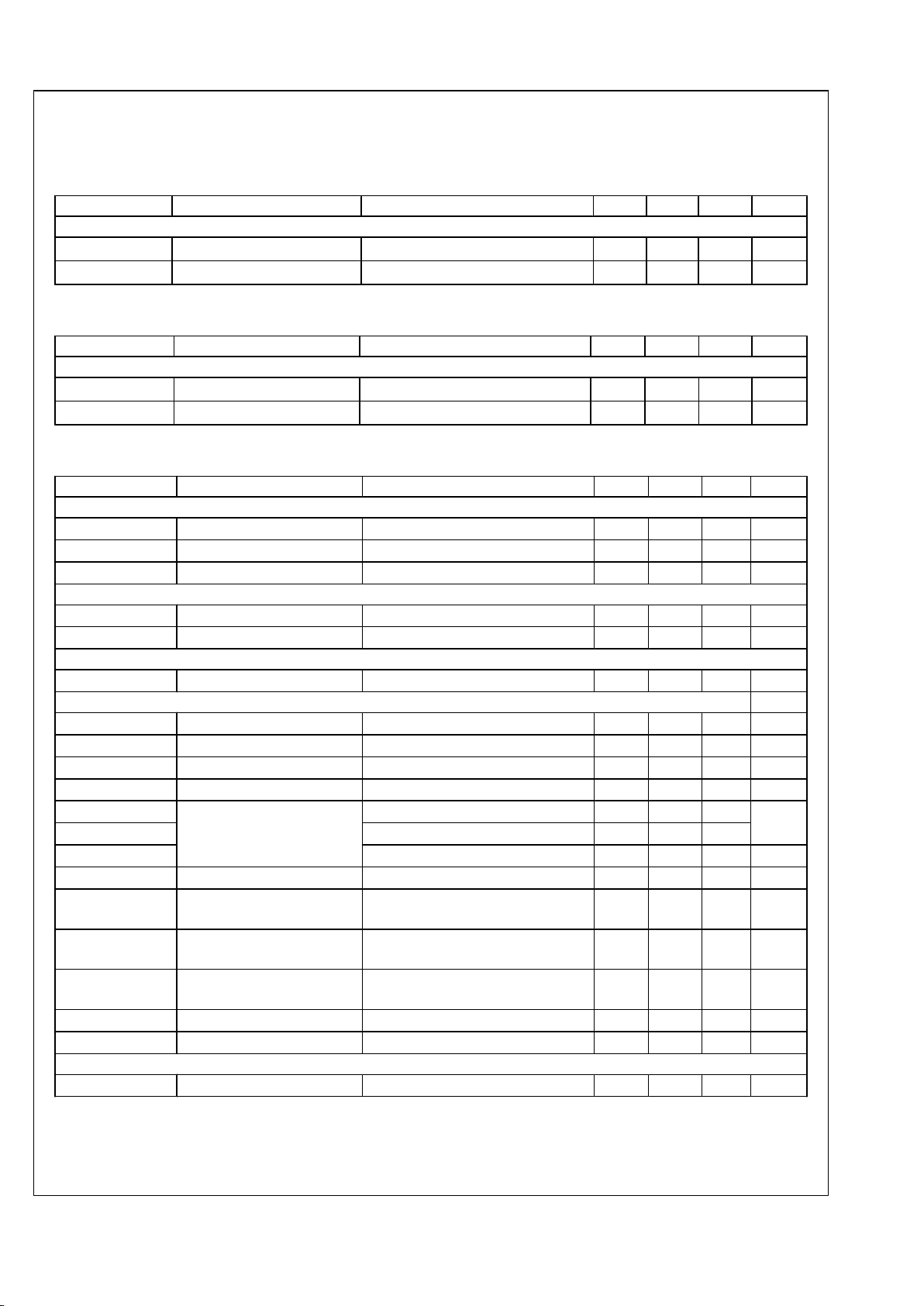
Electrical Characteristics V
IN
= 24V unless otherwise indicated. Typicals and limits appearing in plain type apply
for TA = TJ = +25°C. (Note 4) Limits appearing in boldface type apply over full Operating Temperature Range. Datasheet min/
max specification limits are guaranteed by design, test, or statistical analysis.
LM3404
Symbol Parameter Conditions Min Typ Max Units
SYSTEM PARAMETERS
t
ON-1
On-time 1
VIN = 10V, RON = 200 kΩ
2.1 2.75 3.4 µs
t
ON-2
On-time 2
VIN = 40V, RON = 200 kΩ
515 675 835 ns
LM3404HV
Symbol Parameter Conditions Min Typ Max Units
SYSTEM PARAMETERS
t
ON-1
On-time 1
VIN = 10V, RON = 200 kΩ
2.1 2.75 3.4 µs
t
ON-2
On-time 2
VIN = 70V, RON = 200 kΩ
325 415 505 ns
LM3404/LM3404HV
Symbol Parameter Conditions Min Typ Max Units
REGULATION AND OVER-VOLTAGE COMPARATORS
V
REF-REG
CS Regulation Threshold CS Decreasing, SW turns on 194 200 206 mV
V
REF-0V
CS Over-voltage Threshold CS Increasing, SW turns off 300 mV
I
CS
CS Bias Current CS = 0V 0.1 µA
SHUTDOWN
V
SD-TH
Shutdown Threshold RON / SD Increasing 0.3 0.7 1.05 V
V
SD-HYS
Shutdown Hysteresis RON / SD Decreasing 40 mV
OFF TIMER
t
OFF-MIN
Minimum Off-time CS = 0V 270 ns
INTERNAL REGULATOR
V
CC-REG
VCC Regulated Output 6.4 7 7.4 V
V
IN-DO
VIN - V
CC
ICC = 5 mA, 6.0V < VIN < 8.0V 300 mV
V
CC-BP-TH
VCC Bypass Threshold VIN Increasing 8.8 V
V
CC-BP-HYS
VCC Bypass Hysteresis VIN Decreasing 230 mV
V
CC-Z-6
VCC Output Impedance
(0 mA < ICC < 5 mA)
VIN = 6V 55
Ω
V
CC-Z-8
VIN = 8V 50
V
CC-Z-24
VIN = 24V 0.4
V
CC-LIM
VCC Current Limit (Note 3) VIN = 24V, VCC = 0V 16 mA
V
CC-UV-TH
VCC Under-voltage Lock-out
Threshold
VCC Increasing 5.3 V
V
CC-UV-HYS
VCC Under-voltage Lock-out
Hysteresis
VCC Decreasing 150 mV
V
CC-UV-DLY
VCC Under-voltage Lock-out
Filter Delay
100 mV Overdrive 3 µs
I
IN-OP
I
IN
Operating Current Non-switching, CS = 0.5V 625 900 µA
I
IN-SD
IIN Shutdown Current RON / SD = 0V 95 180 µA
CURRENT LIMIT
I
LIM
Current Limit Threshold 1.2 1.5 1.8 A
5 www.national.com
LM3404/LM3404HV
Page 6
Symbol Parameter Conditions Min Typ Max Units
DIM COMPARATOR
V
IH
Logic High DIM Increasing 2.2 V
V
IL
Logic Low DIM Decreasing 0.8 V
I
DIM-PU
DIM Pull-up Current DIM = 1.5V 80 µA
MOSFET AND DRIVER
R
DS-ON
Buck Switch On Resistance ISW = 200mA, BST-SW = 6.3V 0.37 0.75
Ω
V
DR-UVLO
BST Under-voltage Lock-out
Threshold
BST–SW Increasing 1.7 3 4 V
V
DR-HYS
BST Under-voltage Lock-out
Hysteresis
BST–SW Decreasing 400 mV
THERMAL SHUTDOWN
T
SD
Thermal Shutdown Threshold 165 °C
T
SD-HYS
Thermal Shutdown Hysteresis 25 °C
THERMAL RESISTANCE
θ
JA
Junction to Ambient SOIC-8 Package 155 °C/W
PSOP-8 Package (Note 5) 50
Note 1: Absolute Maximum Ratings indicate limits beyond which damage to the device may occur. Operating Ratings indicate conditions for which the device is
intended to be functional, but specific performance is not guaranteed. For guaranteed specifications and the test conditions, see Electrical Characteristics.
Note 2: The human body model is a 100 pF capacitor discharged through a 1.5 kΩ resistor into each pin.
Note 3: VCC provides self bias for the internal gate drive and control circuits. Device thermal limitations limit external loading.
Note 4: Typical specifications represent the most likely parametric norm at 25°C operation.
Note 5: θJA of 50°C/W with DAP soldered to a minimum of 2 square inches of 1oz. copper on the top or bottom PCB layer.
www.national.com 6
LM3404/LM3404HV
Page 7
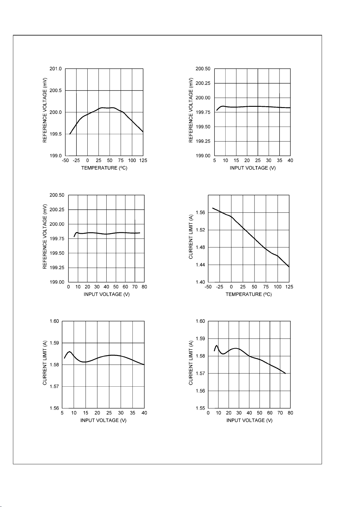
Typical Performance Characteristics
V
REF
vs Temperature (VIN = 24V)
20205450
V
REF
vs VIN, LM3404 (TA = 25°C)
20205451
V
REF
vs VIN, LM3404HV (TA = 25°C)
20205452
Current Limit vs Temperature (VIN = 24V)
20205453
Current Limit vs VIN, LM3404 (TA = 25°C)
20205454
Current Limit vs VIN, LM3404HV (TA = 25°C)
20205455
7 www.national.com
LM3404/LM3404HV
Page 8
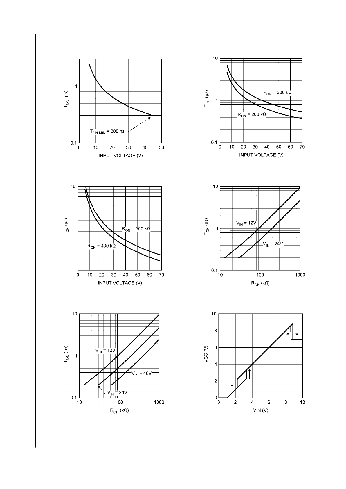
TON vs VIN,
RON = 100 kΩ (TA = 25°C)
20205435
TON vs VIN,
(TA = 25°C)
20205436
TON vs VIN,
(TA = 25°C)
20205437
TON vs RON, LM3404
(TA = 25°C)
20205444
TON vs RON, LM3404HV
(TA = 25°C)
20205438
VCC vs V
IN
(TA = 25°C)
20205439
www.national.com 8
LM3404/LM3404HV
Page 9

V
O-MAX
vs fSW, LM3404
(TA = 25°C)
20205440
V
O-MIN
vs fSW, LM3404
(TA = 25°C)
20205441
V
O-MAX
vs fSW, LM3404HV
(TA = 25°C)
20205442
V
O-MIN
vs fSW, LM3404HV
(TA = 25°C)
20205443
9 www.national.com
LM3404/LM3404HV
Page 10

Block Diagram
20205403
Application Information
THEORY OF OPERATION
The LM3404 and LM3404HV are buck regulators with a wide
input voltage range, low voltage reference, and a fast output
enable/disable function. These features combine to make
them ideal for use as a constant current source for LEDs with
forward currents as high as 1.2A. The controlled on-time
(COT) architecture is a combination of hysteretic mode control and a one-shot on-timer that varies inversely with input
voltage. Hysteretic operation eliminates the need for smallsignal control loop compensation. When the converter runs in
continuous conduction mode (CCM) the controlled on-time
maintains a constant switching frequency over the range of
input voltage. Fast transient response, PWM dimming, a low
power shutdown mode, and simple output overvoltage protection round out the functions of the LM3404/04HV.
CONTROLLED ON-TIME OVERVIEW
Figure 1 shows the feedback system used to control the current through an array of LEDs. A voltage signal, V
SNS
, is
created as the LED current flows through the current setting
resistor, R
SNS
, to ground. V
SNS
is fed back to the CS pin,
where it is compared against a 200 mV reference, V
REF
. The
on-comparator turns on the power MOSFET when V
SNS
falls
below V
REF
. The power MOSFET conducts for a controlled
on-time, tON, set by an external resistor, RON, and by the input
voltage, VIN. On-time is governed by the following equation:
At the conclusion of tON the power MOSFET turns off for a
minimum off-time, t
OFF-MIN
, of 300 ns. Once t
OFF-MIN
is com-
plete the CS comparator compares V
SNS
and V
REF
again,
waiting to begin the next cycle.
20205405
FIGURE 1. Comparator and One-Shot
The LM3404/04HV regulators should be operated in continuous conduction mode (CCM), where inductor current stays
positive throughout the switching cycle. During steady-state
www.national.com 10
LM3404/LM3404HV
Page 11

CCM operation, the converter maintains a constant switching
frequency that can be selected using the following equation:
VF = forward voltage of each LED, n = number of LEDs in
series
AVERAGE LED CURRENT ACCURACY
The COT architecture regulates the valley of ΔV
SNS
, the AC
portion of V
SNS
. To determine the average LED current (which
is also the average inductor current) the valley inductor current is calculated using the following expression:
In this equation t
SNS
represents the propagation delay of the
CS comparator, and is approximately 220 ns. The average
inductor/LED current is equal to I
L-MIN
plus one-half of the in-
ductor current ripple, ΔiL:
IF = IL = I
L-MIN
+ ΔiL / 2
Detailed information for the calculation of ΔiL is given in the
Design Considerations section.
MAXIMUM OUTPUT VOLTAGE
The 300 ns minimum off-time limits the maximum duty cycle
of the converter, D
MAX
, and in turn the maximum output volt-
age, V
O(MAX)
, determined by the following equations:
The maximum number of LEDs, n
MAX
, that can be placed in
a single series string is governed by V
O(MAX)
and the maxi-
mum forward voltage of the LEDs used, V
F(MAX)
, using the
expression:
At low switching frequency the maximum duty cycle and output voltage are higher, allowing the LM3404/04HV to regulate
output voltages that are nearly equal to input voltage. The
following equation relates switching frequency to maximum
output voltage, and is also shown graphically in the Typical
Performance Characteristics section:
MINIMUM OUTPUT VOLTAGE
The minimum recommended on-time for the LM3404/04HV is
300 ns. This lower limit for tON determines the minimum duty
cycle and output voltage that can be regulated based on input
voltage and switching frequency. The relationship is determined by the following equation, shown on the same graphs
as maximum output voltage in the Typical Performance Characteristics section:
HIGH VOLTAGE BIAS REGULATOR
The LM3404/04HV contains an internal linear regulator with
a 7V output, connected between the VIN and the VCC pins.
The VCC pin should be bypassed to the GND pin with a 0.1
µF ceramic capacitor connected as close as possible to the
pins of the IC. VCC tracks VIN until VIN reaches 8.8V (typical)
and then regulates at 7V as VIN increases. Operation begins
when VCC crosses 5.25V.
INTERNAL MOSFET AND DRIVER
The LM3404/04HV features an internal power MOSFET as
well as a floating driver connected from the SW pin to the
BOOT pin. Both rise time and fall time are 20 ns each (typical)
and the approximate gate charge is 6 nC. The high-side rail
for the driver circuitry uses a bootstrap circuit consisting of an
internal high-voltage diode and an external 10 nF capacitor,
CB. VCC charges CB through the internal diode while the power
MOSFET is off. When the MOSFET turns on, the internal
diode reverse biases. This creates a floating supply equal to
the VCC voltage minus the diode drop to drive the MOSFET
when its source voltage is equal to VIN.
FAST SHUTDOWN FOR PWM DIMMING
The DIM pin of the LM3404/04HV is a TTL compatible input
for low frequency PWM dimming of the LED. A logic low (below 0.8V) at DIM will disable the internal MOSFET and shut
off the current flow to the LED array. While the DIM pin is in
a logic low state the support circuitry (driver, bandgap, VCC)
remains active in order to minimize the time needed to turn
the LED array back on when the DIM pin sees a logic high
(above 2.2V). A 75 µA (typical) pull-up current ensures that
the LM3404/04HV is on when DIM pin is open circuited, eliminating the need for a pull-up resistor. Dimming frequency,
f
DIM
, and duty cycle, D
DIM
, are limited by the LED current rise
time and fall time and the delay from activation of the DIM pin
to the response of the internal power MOSFET. In general,
f
DIM
should be at least one order of magnitude lower than the
steady state switching frequency in order to prevent aliasing.
PEAK CURRENT LIMIT
The current limit comparator of the LM3404/04HV will engage
whenever the power MOSFET current (equal to the inductor
current while the MOSFET is on) exceeds 1.5A (typical). The
power MOSFET is disabled for a cool-down time that is approximately 75x the steady-state on-time. At the conclusion
of this cool-down time the system re-starts. If the current limit
condition persists the cycle of cool-down time and restarting
will continue, creating a low-power hiccup mode, minimizing
thermal stress on the LM3404/04HV and the external circuit
components.
OVER-VOLTAGE/OVER-CURRENT COMPARATOR
The CS pin includes an output over-voltage/over-current
comparator that will disable the power MOSFET whenever
11 www.national.com
LM3404/LM3404HV
Page 12

V
SNS
exceeds 300 mV. This threshold provides a hard limit
for the output current. Output current overshoot is limited to
300 mV / R
SNS
by this comparator during transients.
The OVP/OCP comparator can also be used to prevent the
output voltage from rising to V
O(MAX)
in the event of an output
open-circuit. This is the most common failure mode for LEDs,
due to breaking of the bond wires. In a current regulator an
output open circuit causes V
SNS
to fall to zero, commanding
maximum duty cycle. Figure 2 shows a method using a zener
diode, Z1, and zener limiting resistor, RZ, to limit output voltage to the reverse breakdown voltage of Z1 plus 200 mV. The
zener diode reverse breakdown voltage, VZ, must be greater
than the maximum combined VF of all LEDs in the array. The
maximum recommended value for RZ is 1 kΩ.
As discussed in the Maximum Output Voltage section, there
is a limit to how high VO can rise during an output open-circuit
that is always less than VIN. If no output capacitor is used, the
output stage of the LM3404/04HV is capable of withstanding
V
O(MAX)
indefinitely, however the voltage at the output end of
the inductor will oscillate and can go above VIN or below 0V.
A small (typically 10 nF) capacitor across the LED array
dampens this oscillation. For circuits that use an output capacitor, the system can still withstand V
O(MAX)
indefinitely as
long as CO is rated to handle VIN. The high current paths are
blocked in output open-circuit and the risk of thermal stress is
minimal, hence the user may opt to allow the output voltage
to rise in the case of an open-circuit LED failure.
20205412
FIGURE 2. Output Open Circuit Protection
LOW POWER SHUTDOWN
The LM3404/04HV can be placed into a low power state (I
IN-
SD
= 90 µA) by grounding the RON pin with a signal-level
MOSFET as shown in Figure 3. Low power MOSFETs like the
2N7000, 2N3904, or equivalent are recommended devices
for putting the LM3404/04HV into low power shutdown. Logic
gates can also be used to shut down the LM3404/04HV as
long as the logic low voltage is below the over temperature
minimum threshold of 0.3V. Noise filter circuitry on the RON
pin can cause a few pulses with longer on-times than normal
after RON is grounded or released. In these cases the OVP/
OCP comparator will ensure that the peak inductor or LED
current does not exceed 300 mV / R
SNS
.
20205413
FIGURE 3. Low Power Shutdown
www.national.com 12
LM3404/LM3404HV
Page 13

THERMAL SHUTDOWN
Internal thermal shutdown circuitry is provided to protect the
IC in the event that the maximum junction temperature is exceeded. The threshold for thermal shutdown is 165°C with a
25°C hysteresis (both values typical). During thermal shutdown the MOSFET and driver are disabled.
Design Considerations
SWITCHING FREQUENCY
Switching frequency is selected based on the trade-offs between efficiency (better at low frequency), solution size/cost
(smaller at high frequency), and the range of output voltage
that can be regulated (wider at lower frequency.) Many applications place limits on switching frequency due to EMI sensitivity. The on-time of the LM3404/04HV can be programmed
for switching frequencies ranging from the 10’s of kHz to over
1 MHz. The maximum switching frequency is limited only by
the minimum on-time and minimum off-time requirements.
LED RIPPLE CURRENT
Selection of the ripple current, ΔiF, through the LED array is
analogous to the selection of output ripple voltage in a standard voltage regulator. Where the output ripple in a voltage
regulator is commonly ±1% to ±5% of the DC output voltage,
LED manufacturers generally recommend values for Δi
F
ranging from ±5% to ±20% of IF. Higher LED ripple current
allows the use of smaller inductors, smaller output capacitors,
or no output capacitors at all. The advantages of higher ripple
current are reduction in the solution size and cost. Lower ripple current requires more output inductance, higher switching
frequency, or additional output capacitance. The advantages
of lower ripple current are a reduction in heating in the LED
itself and greater tolerance in the average LED current before
the current limit of the LED or the driving circuitry is reached.
BUCK CONVERTERS WITHOUT OUTPUT CAPACITORS
The buck converter is unique among non-isolated topologies
because of the direct connection of the inductor to the load
during the entire switching cycle. By definition an inductor will
control the rate of change of current that flows through it, and
this control over current ripple forms the basis for component
selection in both voltage regulators and current regulators. A
current regulator such as the LED driver for which the
LM3404/04HV was designed focuses on the control of the
current through the load, not the voltage across it. A constant
current regulator is free of load current transients, and has no
need of output capacitance to supply the load and maintain
output voltage. Referring to the Typical Application circuit on
the front page of this datasheet, the inductor and LED can
form a single series chain, sharing the same current. When
no output capacitor is used, the same equations that govern
inductor ripple current, ΔiL, also apply to the LED ripple current, ΔiF. For a controlled on-time converter such as
LM3404/04HV the ripple current is described by the following
expression:
A minimum ripple voltage of 25 mV is recommended at the
CS pin to provide good signal to noise ratio (SNR). The CS
pin ripple voltage, Δv
SNS
, is described by the following:
Δv
SNS
= ΔiF x R
SNS
BUCK CONVERTERS WITH OUTPUT CAPACITORS
A capacitor placed in parallel with the LED or array of LEDs
can be used to reduce the LED current ripple while keeping
the same average current through both the inductor and the
LED array. This technique is demonstrated in Design Examples 1 and 2. With this topology the output inductance can be
lowered, making the magnetics smaller and less expensive.
Alternatively, the circuit could be run at lower frequency but
keep the same inductor value, improving the efficiency and
expanding the range of output voltage that can be regulated.
Both the peak current limit and the OVP/OCP comparator still
monitor peak inductor current, placing a limit on how large
ΔiL can be even if ΔiF is made very small. A parallel output
capacitor is also useful in applications where the inductor or
input voltage tolerance is poor. Adding a capacitor that reduces ΔiF to well below the target provides headroom for
changes in inductance or VIN that might otherwise push the
peak LED ripple current too high.
Figure 4 shows the equivalent impedances presented to the
inductor current ripple when an output capacitor, CO, and its
equivalent series resistance (ESR) are placed in parallel with
the LED array. The entire inductor ripple current flows through
R
SNS
to provide the required 25 mV of ripple voltage for proper
operation of the CS comparator.
20205415
FIGURE 4. LED and CO Ripple Current
To calculate the respective ripple currents the LED array is
represented as a dynamic resistance, rD. LED dynamic resistance is not always specified on the manufacturer’s
datasheet, but it can be calculated as the inverse slope of the
LED’s VF vs. IF curve. Note that dividing VF by IF will give an
incorrect value that is 5x to 10x too high. Total dynamic resistance for a string of n LEDs connected in series can be
calculated as the rD of one device multiplied by n. Inductor
ripple current is still calculated with the expression from Buck
Regulators without Output Capacitors. The following equations can then be used to estimate ΔiF when using a parallel
capacitor:
The calculation for ZC assumes that the shape of the inductor
ripple current is approximately sinusoidal.
13 www.national.com
LM3404/LM3404HV
Page 14

Small values of CO that do not significantly reduce ΔiF can
also be used to control EMI generated by the switching action
of the LM3404/04HV. EMI reduction becomes more important
as the length of the connections between the LED and the
rest of the circuit increase.
INPUT CAPACITORS
Input capacitors at the VIN pin of the LM3404/04HV are selected using requirements for minimum capacitance and rms
ripple current. The input capacitors supply pulses of current
approximately equal to IF while the power MOSFET is on, and
are charged up by the input voltage while the power MOSFET
is off. Switching converters such as the LM3404/04HV have
a negative input impedance due to the decrease in input current as input voltage increases. This inverse proportionality of
input current to input voltage can cause oscillations (sometimes called ‘power supply interaction’) if the magnitude of the
negative input impedance is greater the the input filter
impedance. Minimum capacitance can be selected by comparing the input impedance to the converter’s negative resistance; however this requires accurate calculation of the input
voltage source inductance and resistance, quantities which
can be difficult to determine. An alternative method to select
the minimum input capacitance, C
IN(MIN)
, is to select the max-
imum input voltage ripple which can be tolerated. This value,
Δv
IN(MAX)
, is equal to the change in voltage across CIN during
the converter on-time, when CIN supplies the load current.
C
IN(MIN)
can be selected with the following:
A good starting point for selection of CIN is to use an input
voltage ripple of 5% to 10% of VIN. A minimum input capacitance of 2x the C
IN(MIN)
value is recommended for all
LM3404/04HV circuits. To determine the rms current rating,
the following formula can be used:
Ceramic capacitors are the best choice for the input to the
LM3404/04HV due to their high ripple current rating, low ESR,
low cost, and small size compared to other types. When selecting a ceramic capacitor, special attention must be paid to
the operating conditions of the application. Ceramic capacitors can lose one-half or more of their capacitance at their
rated DC voltage bias and also lose capacitance with extremes in temperature. A DC voltage rating equal to twice the
expected maximum input voltage is recommended. In addition, the minimum quality dielectric which is suitable for
switching power supply inputs is X5R, while X7R or better is
preferred.
RECIRCULATING DIODE
The LM3404/04HV is a non-synchronous buck regulator that
requires a recirculating diode D1 (see the Typical Application
circuit) to carrying the inductor current during the MOSFET
off-time. The most efficient choice for D1 is a Schottky diode
due to low forward drop and near-zero reverse recovery time.
D1 must be rated to handle the maximum input voltage plus
any switching node ringing when the MOSFET is on. In practice all switching converters have some ringing at the switching node due to the diode parasitic capacitance and the lead
inductance. D1 must also be rated to handle the average current, ID, calculated as:
ID = (1 – D) x I
F
This calculation should be done at the maximum expected
input voltage. The overall converter efficiency becomes more
dependent on the selection of D1 at low duty cycles, where
the recirculating diode carries the load current for an increasing percentage of the time. This power dissipation can be
calculating by checking the typical diode forward voltage,
VD, from the I-V curve on the product datasheet and then
multiplying it by ID. Diode datasheets will also provide a typical
junction-to-ambient thermal resistance, θJA, which can be
used to estimate the operating die temperature of the device.
Multiplying the power dissipation (PD = ID x VD) by θ
JA
gives
the temperature rise. The diode case size can then be selected to maintain the Schottky diode temperature below the
operational maximum.
Design Example 1: LM3404
The first example circuit will guide the user through component selection for an architectural accent lighting application.
A regulated DC voltage input of 24V ±10% will power a 5.4W
"warm white" LED module that consists of four LEDs in a 2 x
2 series-parallel configuration. The module will be treated as
a two-terminal element and driven with a forward current of
700 mA ±5%. The typical forward voltage of the LED module
in thermal steady state is 6.9V, hence the average output
voltage will be 7.1V. The objective of this application is to
place the complete current regulator and LED module in a
compact space formerly occupied by a halogen light source.
(The LED will be on a separate metal-core PCB and heatsink.)
Switching frequency will be 400 kHz to keep switching loss
low, as the confined space with no air-flow requires a maximum temperature rise of 50°C in each circuit component. A
small solution size is also important, as the regulator must fit
on a circular PCB with a 1.5" diameter. A complete bill of materials can be found in Table 1 at the end of this datasheet.
www.national.com 14
LM3404/LM3404HV
Page 15

20205419
FIGURE 5. Schematic for Design Example 1
RON and t
ON
A moderate switching frequency is needed in this application
to balance the requirements of magnetics size and efficiency.
RON is selected from the equation for switching frequency as
follows:
RON = 7.1 / (1.34 x 10
-10
x 4 x 105) = 132.5 kΩ
The closest 1% tolerance resistor is 133 kΩ. The switching
frequency and on-time of the circuit can then be found using
the equations relating RON and tON to fSW:
fSW = 7.1 / (1.33 x 105 x 1.34 x 10
-10
) = 398 kHz
tON = (1.34 x 10
-10
x 1.33 x 105) / 24 = 743 ns
OUTPUT INDUCTOR
Since an output capacitor will be used to filter some of the AC
ripple current, the inductor ripple current can be set higher
than the LED ripple current. A value of 40%
P-P
is typical in
many buck converters:
ΔiL = 0.4 x 0.7 = 0.28A
With the target ripple current determined the inductance can
be chosen:
L
MIN
= [(24 – 7.1) x 7.43 x 10-7] / (0.28) = 44.8 µH
The closest standard inductor value is 47 µH. The average
current rating should be greater than 700 mA to prevent overheating in the inductor. Separation between the LM3404
drivers and the LED arrays means that heat from the inductor
will not threaten the lifetime of the LEDs, but an overheated
inductor could still cause the LM3404 to enter thermal shutdown.
The inductance of the standard part chosen is ±20%. With this
tolerance the typical, minimum, and maximum inductor current ripples can be calculated:
Δi
L(TYP)
= [(24 - 7.1) x 7.43 x 10-7] / 47 x 10
-6
= 266 mA
P-P
Δi
L(MIN)
= [(24 - 7.1) x 7.43 x 10-7] / 56 x 10
-6
= 223 mA
P-P
Δi
L(MAX)
= [(24 - 7.1) x 7.43 x 10-7] / 38 x 10
-6
= 330 mA
P-P
The peak LED/inductor current is then estimated:
I
L(PEAK)
= IL + 0.5 x Δi
L(MAX)
I
L(PEAK)
= 0.7 + 0.5 x 0.330 = 866 mA
In the case of a short circuit across the LED array, the LM3404
will continue to deliver rated current through the short but will
reduce the output voltage to equal the CS pin voltage of 200
mV. The inductor ripple current and peak current in this condition would be equal to:
Δi
L(LED-SHORT)
= [(24 – 0.2) x 7.43 x 10-7] / 38 x 10
-6
= 465 mA
P-P
I
L(PEAK)
= 0.7 + 0.5 x 0.465 = 933 mA
In the case of a short at the switch node, the output, or from
the CS pin to ground the short circuit current limit will engage
15 www.national.com
LM3404/LM3404HV
Page 16

at a typical peak current of 1.5A. In order to prevent inductor
saturation during these fault conditions the inductor’s peak
current rating must be above 1.5A. A 47 µH off-the shelf inductor rated to 1.4A (peak) and 1.5A (average) with a DCR of
0.1Ω will be used.
USING AN OUTPUT CAPACITOR
This application does not require high frequency PWM dimming, allowing the use of an output capacitor to reduce the
size and cost of the output inductor. To select the proper output capacitor the equation from Buck Regulators with Output
Capacitors is re-arranged to yield the following:
The target tolerance for LED ripple current is 100 mA
P-P
, and
a typical value for rD of 1.8Ω at 700 mA can be read from the
LED datasheet. The required capacitor impedance to reduce
the worst-case inductor ripple current of 333 mA
P-P
is there-
fore:
ZC = [0.1 / (0.333 - 0.1] x 1.8 = 0.77Ω
A ceramic capacitor will be used and the required capacitance
is selected based on the impedance at 400 kHz:
CO = 1/(2 x π x 0.77 x 4 x 105) = 0.51 µF
This calculation assumes that impedance due to the equivalent series resistance (ESR) and equivalent series inductance
(ESL) of CO is negligible. The closest 10% tolerance capacitor
value is 1.0 µF. The capacitor used should be rated to 25V or
more and have an X7R dielectric. Several manufacturers produce ceramic capacitors with these specifications in the 0805
case size. A typical value for ESR of 3 mΩ can be read from
the curve of impedance vs. frequency in the product
datasheet.
R
SNS
A preliminary value for R
SNS
was determined in selecting
ΔiL. This value should be re-evaluated based on the calcula-
tions for ΔiF:
t
SNS
= 220 ns, R
SNS
= 0.33Ω
Sub-1Ω resistors are available in both 1% and 5% tolerance.
A 1%, 0.33Ω device is the closest value, and a 0.33W, 1206
size device will handle the power dissipation of 162 mW. With
the resistance selected, the average value of LED current is
re-calculated to ensure that current is within the ±5% tolerance requirement. From the expression for average LED
current:
IF = 0.2 / 0.33 - (7.1 x 2.2 x 10-7) / 47 x 10-6 + 0.266 / 2
= 706 mA, 1% above 700 mA
INPUT CAPACITOR
Following the calculations from the Input Capacitor section,
Δv
IN(MAX)
will be 24V x 2%
P-P
= 480 mV. The minimum re-
quired capacitance is:
C
IN(MIN)
= (0.7 x 7.4 x 10-7) / 0.48 = 1.1 µF
To provide additional safety margin the a higher value of 3.3
µF ceramic capacitor rated to 50V with X7R dielectric in an
1210 case size will be used. From the Design Considerations
section, input rms current is:
I
IN-RMS
= 0.7 x Sqrt(0.28 x 0.72) = 314 mA
Ripple current ratings for 1210 size ceramic capacitors are
typically higher than 2A, more than enough for this design.
RECIRCULATING DIODE
The input voltage of 24V ±5% requires Schottky diodes with
a reverse voltage rating greater than 30V. The next highest
standard voltage rating is 40V. Selecting a 40V rated diode
provides a large safety margin for the ringing of the switch
node and also makes cross-referencing of diodes from different vendors easier.
The next parameters to be determined are the forward current
rating and case size. In this example the low duty cycle (D =
7.1 / 24 = 28%) places a greater thermal stress on D1 than
on the internal power MOSFET of the LM3404. The estimated
average diode current is:
ID = 0.706 x 0.72 = 509 mA
A Schottky with a forward current rating of 1A would be adequate, however reducing the power dissipation is critical in
this example. Higher current diodes have lower forward voltages, hence a 2A-rated diode will be used. To determine the
proper case size, the dissipation and temperature rise in D1
can be calculated as shown in the Design Considerations
section. VD for a case size such as SMB in a 40V, 2A Schottky
diode at 700 mA is approximately 0.3V and the θJA is 75°C/
W. Power dissipation and temperature rise can be calculated
as:
PD = 0.509 x 0.3 = 153 mW
T
RISE
= 0.153 x 75 = 11.5°C
CB AND C
F
The bootstrap capacitor CB should always be a 10 nF ceramic
capacitor with X7R dielectric. A 25V rating is appropriate for
all application circuits. The linear regulator filter capacitor C
F
should always be a 100 nF ceramic capacitor, also with X7R
dielectric and a 25V rating.
EFFICIENCY
To estimate the electrical efficiency of this example the power
dissipation in each current carrying element can be calculated
and summed. Electrical efficiency, η, should not be confused
www.national.com 16
LM3404/LM3404HV
Page 17

with the optical efficacy of the circuit, which depends upon the
LEDs themselves.
Total output power, PO, is calculated as:
PO = IF x VO = 0.706 x 7.1 = 5W
Conduction loss, PC, in the internal MOSFET:
PC = (I
F
2
x R
DSON
) x D = (0.7062 x 0.8) x 0.28 = 112 mW
Gate charging and VCC loss, PG, in the gate drive and linear
regulator:
PG = (I
IN-OP
+ fSW x QG) x V
IN
PG = (600 x 10-6 + 4 x 105 x 6 x 10-9) x 24 = 72 mW
Switching loss, PS, in the internal MOSFET:
PS = 0.5 x VIN x IF x (tR + tF) x f
SW
PS = 0.5 x 24 x 0.706 x 40 x 10-9 x 4 x 105 = 136 mW
AC rms current loss, P
CIN
, in the input capacitor:
P
CIN
= I
IN(rms)
2
x ESR = 0.3172 0.003 = 0.3 mW (negligible)
DCR loss, PL, in the inductor
PL = I
F
2
x DCR = 0.7062 x 0.1 = 50 mW
Recirculating diode loss, PD = 153 mW
Current Sense Resistor Loss, P
SNS
= 164 mW
Electrical efficiency, η = PO / (PO + Sum of all loss terms) =
5 / (5 + 0.687) = 88%
Temperature Rise in the LM3404 IC is calculated as:
T
LM3404
= (PC + PG + PS) x θJA = (0.112 + 0.072 + 0.136) x
155 = 49.2°C
Design Example 2: LM3404HV
The second example circuit will guide the user through component selection for an outdoor general lighting application.
A regulated DC voltage input of 48V ±10% will power ten series-connected LEDs at 500 mA ±10% with a ripple current of
50 mA
P-P
or less. The typical forward voltage of the LED module in thermal steady state is 35V, hence the average output
voltage will be 35.2V. A complete bill of materials can be found
in Table 2 at the end of this datasheet.
20205432
FIGURE 6. Schematic for Design Example 2
RON and t
ON
A low switching frequency, 225 kHz, is needed in this application, as high efficiency and low power dissipation take
precedence over the solution size. RON is selected from the
equation for switching frequency as follows:
RON = 35.2 / (1.34 x 10
-10
x 2.25 x 105) = 1.16 MΩ
The next highest 1% tolerance resistor is 1.18 MΩ. The
switching frequency and on-time of the circuit can then be
found using the equations relating RON and tON to fSW:
fSW = 35.2 / (1.18 x 106 x 1.34 x 10
-10
) = 223 kHz
tON = (1.34 x 10
-10
x 1.18 x 106) / 48 = 3.3 µs
OUTPUT INDUCTOR
Since an output capacitor will be used to filter some of the AC
ripple current, the inductor ripple current can be set higher
than the LED ripple current. A value of 30%
P-P
makes a good
trade-off between the current ripple and the size of the inductor:
ΔiL = 0.3 x 0.5 = 0.15A
17 www.national.com
LM3404/LM3404HV
Page 18

With the target ripple current determined the inductance can
be chosen:
L
MIN
= [(48 – 35.2) x 3.3 x 10-6] / (0.15) = 281 µH
The closest standard inductor value above 281 is 330 µH. The
average current rating should be greater than 0.5A to prevent
overheating in the inductor. In this example the LM3404HV
driver and the LED array share the same metal-core PCB,
meaning that heat from the inductor could threaten the lifetime
of the LEDs. For this reason the average current rating of the
inductor used should have a de-rating of about 50%, or 1A.
The inductance of the standard part chosen is ±20%. With this
tolerance the typical, minimum, and maximum inductor current ripples can be calculated:
Δi
L(TYP)
= [(48 - 35.2) x 3.3 x 10-6] / 330 x 10
-6
= 128 mA
P-P
Δi
L(MIN)
= [(48 - 35.2) x 3.3 x 10-6] / 396 x 10
-6
= 107 mA
P-P
Δi
L(MAX)
= [(48 - 35.2) x 3.3 x 10-6] / 264 x 10
-6
= 160 mA
P-P
The peak inductor current is then estimated:
I
L(PEAK)
= IL + 0.5 x Δi
L(MAX)
I
L(PEAK)
= 0.5 + 0.5 x 0.16 = 0.58A
In the case of a short circuit across the LED array, the
LM3404HV will continue to deliver rated current through the
short but will reduce the output voltage to equal the CS pin
voltage of 200 mV. The inductor ripple current and peak current in this condition would be equal to:
Δi
L(LED-SHORT)
= [(48 – 0.2) x 3.3 x 10-6] / 264 x 10
-6
= 0.598A
P-P
I
L(PEAK)
= 0.5 + 0.5 x 0.598 = 0.8A
In the case of a short at the switch node, the output, or from
the CS pin to ground the short circuit current limit will engage
at a typical peak current of 1.5A. In order to prevent inductor
saturation during these fault conditions the inductor’s peak
current rating must be above 1.5A. A 330 µH off-the shelf inductor rated to 1.9A (peak) and 1.0A (average) with a DCR of
0.56Ω will be used.
USING AN OUTPUT CAPACITOR
This application uses sub-1 kHz frequency PWM dimming,
allowing the use of a small output capacitor to reduce the size
and cost of the output inductor. To select the proper output
capacitor the equation from Buck Regulators with Output Capacitors is re-arranged to yield the following:
The target tolerance for LED ripple current is 50 mA
P-P
, and
the typical value for rD is 10Ω with ten LEDs in series. The
required capacitor impedance to reduce the worst-case
steady-state inductor ripple current of 160 mA
P-P
is therefore:
ZC = [0.05 / (0.16 - 0.05] x 10 = 4.5Ω
A ceramic capacitor will be used and the required capacitance
is selected based on the impedance at 223 kHz:
CO = 1/(2 x π x 4.5 x 2.23 x 105) = 0.16 µF
This calculation assumes that impedance due to the equivalent series resistance (ESR) and equivalent series inductance
(ESL) of CO is negligible. The closest 10% tolerance capacitor
value is 0.15 µF. The capacitor used should be rated to 50V
or more and have an X7R dielectric. Several manufacturers
produce ceramic capacitors with these specifications in the
0805 case size. ESR values are not typically provided for such
low value capacitors, however is can be assumed to be under
100 mΩ, leaving plenty of margin to meet to LED ripple current
requirement. The low capacitance required allows the use of
a 100V rated, 1206-size capacitor. The rating of 100V ensures that the capacitance will not decrease significantly
when the DC output voltage is applied across the capacitor.
R
SNS
A preliminary value for R
SNS
was determined in selecting
ΔiL. This value should be re-evaluated based on the calcula-
tions for ΔiF:
t
SNS
= 220 ns, R
SNS
= 0.43Ω
Sub-1Ω resistors are available in both 1% and 5% tolerance.
A 1%, 0.43Ω device is the closest value, and a 0.25W, 0805
size device will handle the power dissipation of 110 mW. With
the resistance selected, the average value of LED current is
re-calculated to ensure that current is within the ±10% tolerance requirement. From the expression for average LED
current:
IF = 0.2 / 0.43 - (35.2 x 2.2 x 10-7) / 330 x 10-6 + 0.128 / 2
= 505 mA
www.national.com 18
LM3404/LM3404HV
Page 19

INPUT CAPACITOR
Following the calculations from the Input Capacitor section,
Δv
IN(MAX)
will be 48V x 2%
P-P
= 960 mV. The minimum re-
quired capacitance is:
C
IN(MIN)
= (0.5 x 3.3 x 10-6) / 0.96 = 1.7 µF
To provide additional safety margin a 2.2 µF ceramic capacitor rated to 100V with X7R dielectric in an 1812 case size will
be used. From the Design Considerations section, input rms
current is:
I
IN-RMS
= 0.5 x Sqrt(0.73 x 0.27) = 222 mA
Ripple current ratings for 1812 size ceramic capacitors are
typically higher than 2A, more than enough for this design,
and the ESR is approximately 3 mΩ.
RECIRCULATING DIODE
The input voltage of 48V requires Schottky diodes with a reverse voltage rating greater than 50V. The next highest standard voltage rating is 60V. Selecting a 60V rated diode
provides a large safety margin for the ringing of the switch
node and also makes cross-referencing of diodes from different vendors easier.
The next parameters to be determined are the forward current
rating and case size. In this example the high duty cycle (D =
35.2 / 48 = 73%) places a greater thermal stress on the internal power MOSFET than on D1. The estimated average
diode current is:
ID = 0.5 x 0.27 = 135 mA
A Schottky with a forward current rating of 0.5A would be adequate, however reducing the power dissipation is critical in
this example. Higher current diodes have lower forward voltages, hence a 1A-rated diode will be used. To determine the
proper case size, the dissipation and temperature rise in D1
can be calculated as shown in the Design Considerations
section. VD for a case size such as SMA in a 60V, 1A Schottky
diode at 0.5A is approximately 0.35V and the θJA is 75°C/W.
Power dissipation and temperature rise can be calculated as:
PD = 0.135 x 0.35 = 47 mW
T
RISE
= 0.047 x 75 = 3.5°C
CB AND C
F
The bootstrap capacitor CB should always be a 10 nF ceramic
capacitor with X7R dielectric. A 25V rating is appropriate for
all application circuits. The linear regulator filter capacitor C
F
should always be a 100 nF ceramic capacitor, also with X7R
dielectric and a 25V rating.
EFFICIENCY
To estimate the electrical efficiency of this example the power
dissipation in each current carrying element can be calculated
and summed. Electrical efficiency, η, should not be confused
with the optical efficacy of the circuit, which depends upon the
LEDs themselves.
Total output power, PO, is calculated as:
PO = IF x VO = 0.5 x 35.2 = 17.6W
Conduction loss, PC, in the internal MOSFET:
PC = (I
F
2
x R
DSON
) x D = (0.52 x 0.8) x 0.73 = 146 mW
Gate charging and VCC loss, PG, in the gate drive and linear
regulator:
PG = (I
IN-OP
+ fSW x QG) x V
IN
PG = (600 x 10-6 + 2.23 x 105 x 6 x 10-9) x 48 = 94 mW
Switching loss, PS, in the internal MOSFET:
PS = 0.5 x VIN x IF x (tR + tF) x f
SW
PS = 0.5 x 48 x 0.5 x 40 x 10-9 x 2.23 x 105 = 107 mW
AC rms current loss, P
CIN
, in the input capacitor:
P
CIN
= I
IN(rms)
2
x ESR = 0.2222 0.003 = 0.1 mW (negligible)
DCR loss, PL, in the inductor
PL = I
F
2
x DCR = 0.52 x 0.56 = 140 mW
Recirculating diode loss, PD = 47 mW
Current Sense Resistor Loss, P
SNS
= 110 mW
Electrical efficiency, η = PO / (PO + Sum of all loss terms) =
17.6 / (17.6 + 0.644) = 96%
Temperature Rise in the LM3404HV IC is calculated as:
T
LM3404
= (PC + PG + PS) x θJA = (0.146 + 0.094 + 0.107) x
155 = 54°C
Layout Considerations
The performance of any switching converter depends as
much upon the layout of the PCB as the component selection.
The following guidelines will help the user design a circuit with
maximum rejection of outside EMI and minimum generation
of unwanted EMI.
COMPACT LAYOUT
Parasitic inductance can be reduced by keeping the power
path components close together and keeping the area of the
loops that high currents travel small. Short, thick traces or
copper pours (shapes) are best. In particular, the switch node
(where L1, D1, and the SW pin connect) should be just large
enough to connect all three components without excessive
heating from the current it carries. The LM3404/04HV operates in two distinct cycles whose high current paths are shown
in Figure 7:
19 www.national.com
LM3404/LM3404HV
Page 20

20205428
FIGURE 7. Buck Converter Current Loops
The dark grey, inner loop represents the high current path
during the MOSFET on-time. The light grey, outer loop represents the high current path during the off-time.
GROUND PLANE AND SHAPE ROUTING
The diagram of Figure 7 is also useful for analyzing the flow
of continuous current vs. the flow of pulsating currents. The
circuit paths with current flow during both the on-time and offtime are considered to be continuous current, while those that
carry current during the on-time or off-time only are pulsating
currents. Preference in routing should be given to the pulsating current paths, as these are the portions of the circuit most
likely to emit EMI. The ground plane of a PCB is a conductor
and return path, and it is susceptible to noise injection just as
any other circuit path. The continuous current paths on the
ground net can be routed on the system ground plane with
less risk of injecting noise into other circuits. The path between the input source and the input capacitor and the path
between the recirculating diode and the LEDs/current sense
resistor are examples of continuous current paths. In contrast,
the path between the recirculating diode and the input capacitor carries a large pulsating current. This path should be
routed with a short, thick shape, preferably on the component
side of the PCB. Multiple vias in parallel should be used right
at the pad of the input capacitor to connect the component
side shapes to the ground plane. A second pulsating current
loop that is often ignored is the gate drive loop formed by the
SW and BOOT pins and capacitor CB. To minimize this loop
at the EMI it generates, keep CB close to the SW and BOOT
pins.
CURRENT SENSING
The CS pin is a high-impedance input, and the loop created
by R
SNS
, RZ (if used), the CS pin and ground should be made
as small as possible to maximize noise rejection. R
SNS
should
therefore be placed as close as possible to the CS and GND
pins of the IC.
REMOTE LED ARRAYS
In some applications the LED or LED array can be far away
(several inches or more) from the LM3404/04HV, or on a separate PCB connected by a wiring harness. When an output
capacitor is used and the LED array is large or separated from
the rest of the converter, the output capacitor should be
placed close to the LEDs to reduce the effects of parasitic
inductance on the AC impedance of the capacitor. The current
sense resistor should remain on the same PCB, close to the
LM3404/04HV.
www.national.com 20
LM3404/LM3404HV
Page 21

TABLE 1. BOM for Design Example 1
ID Part Number Type Size Parameters Qty Vendor
U1 LM3404 LED Driver SO-8 42V, 1.2A 1 NSC
L1 SLF10145T-470M1R4 Inductor 10 x 10 x 4.5mm 47 µH, 1.4A, 120
mΩ
1 TDK
D1 CMSH2-40 Schottky Diode SMB 40V, 2A 1 Central Semi
Cf VJ0805Y104KXXAT Capacitor 0805 100 nF 10% 1 Vishay
Cb VJ0805Y103KXXAT Capacitor 0805 10 nF 10% 1 Vishay
Cin C3225X7R1H335M Capacitor 1210 3.3 µF, 50V 1 TDK
Co C2012X7R1E105M Capacitor 0805 1.0 µF, 25V 1 TDK
Rsns ERJ8BQFR33V Resistor 1206
0.33Ω 1%
1 Panasonic
Ron CRCW08051333F Resistor 0805
133 kΩ 1%
1 Vishay
TABLE 2. BOM for Design Example 2
ID Part Number Type Size Parameters Qty Vendor
U1 LM3404HV LED Driver SO-8 75V, 1.2A 1 NSC
L1 DO5022P-334 Inductor 18.5 x 15.4 x 7.1mm 330 µH, 1.9A,
0.56Ω
1 Coilcraft
D1 CMSH1-60M Schottky Diode SMA 60V, 1A 1 Central Semi
Cf VJ0805Y104KXXAT Capacitor 0805 100 nF 10% 1 Vishay
Cb VJ0805Y103KXXAT Capacitor 0805 10 nF 10% 1 Vishay
Cin C4532X7R2A225M Capacitor 1812 2.2 µF, 100V 1 TDK
Co C3216X7R2A154M Capacitor 1206 0.15 µF, 100V 1 TDK
Rsns ERJ6BQFR43V Resistor 0805
0.43Ω 1%
1 Panasonic
Ron CRCW08051184F Resistor 0805
1.18 MΩ 1%
1 Vishay
21 www.national.com
LM3404/LM3404HV
Page 22

Physical Dimensions inches (millimeters) unless otherwise noted
SO-8 Package
NS Package Number M08A
PSOP-8 Package
NS Package Number MRA08B
www.national.com 22
LM3404/LM3404HV
Page 23

Notes
23 www.national.com
LM3404/LM3404HV
Page 24

Notes
LM3404/04HV 1.0A Constant Current Buck Regulator for Driving High Power LEDs
THE CONTENTS OF THIS DOCUMENT ARE PROVIDED IN CONNECTION WITH NATIONAL SEMICONDUCTOR CORPORATION
(“NATIONAL”) PRODUCTS. NATIONAL MAKES NO REPRESENTATIONS OR WARRANTIES WITH RESPECT TO THE ACCURACY
OR COMPLETENESS OF THE CONTENTS OF THIS PUBLICATION AND RESERVES THE RIGHT TO MAKE CHANGES TO
SPECIFICATIONS AND PRODUCT DESCRIPTIONS AT ANY TIME WITHOUT NOTICE. NO LICENSE, WHETHER EXPRESS,
IMPLIED, ARISING BY ESTOPPEL OR OTHERWISE, TO ANY INTELLECTUAL PROPERTY RIGHTS IS GRANTED BY THIS
DOCUMENT.
TESTING AND OTHER QUALITY CONTROLS ARE USED TO THE EXTENT NATIONAL DEEMS NECESSARY TO SUPPORT
NATIONAL’S PRODUCT WARRANTY. EXCEPT WHERE MANDATED BY GOVERNMENT REQUIREMENTS, TESTING OF ALL
PARAMETERS OF EACH PRODUCT IS NOT NECESSARILY PERFORMED. NATIONAL ASSUMES NO LIABILITY FOR
APPLICATIONS ASSISTANCE OR BUYER PRODUCT DESIGN. BUYERS ARE RESPONSIBLE FOR THEIR PRODUCTS AND
APPLICATIONS USING NATIONAL COMPONENTS. PRIOR TO USING OR DISTRIBUTING ANY PRODUCTS THAT INCLUDE
NATIONAL COMPONENTS, BUYERS SHOULD PROVIDE ADEQUATE DESIGN, TESTING AND OPERATING SAFEGUARDS.
EXCEPT AS PROVIDED IN NATIONAL’S TERMS AND CONDITIONS OF SALE FOR SUCH PRODUCTS, NATIONAL ASSUMES NO
LIABILITY WHATSOEVER, AND NATIONAL DISCLAIMS ANY EXPRESS OR IMPLIED WARRANTY RELATING TO THE SALE
AND/OR USE OF NATIONAL PRODUCTS INCLUDING LIABILITY OR WARRANTIES RELATING TO FITNESS FOR A PARTICULAR
PURPOSE, MERCHANTABILITY, OR INFRINGEMENT OF ANY PATENT, COPYRIGHT OR OTHER INTELLECTUAL PROPERTY
RIGHT.
LIFE SUPPORT POLICY
NATIONAL’S PRODUCTS ARE NOT AUTHORIZED FOR USE AS CRITICAL COMPONENTS IN LIFE SUPPORT DEVICES OR
SYSTEMS WITHOUT THE EXPRESS PRIOR WRITTEN APPROVAL OF THE CHIEF EXECUTIVE OFFICER AND GENERAL
COUNSEL OF NATIONAL SEMICONDUCTOR CORPORATION. As used herein:
Life support devices or systems are devices which (a) are intended for surgical implant into the body, or (b) support or sustain life and
whose failure to perform when properly used in accordance with instructions for use provided in the labeling can be reasonably expected
to result in a significant injury to the user. A critical component is any component in a life support device or system whose failure to perform
can be reasonably expected to cause the failure of the life support device or system or to affect its safety or effectiveness.
National Semiconductor and the National Semiconductor logo are registered trademarks of National Semiconductor Corporation. All other
brand or product names may be trademarks or registered trademarks of their respective holders.
Copyright© 2007 National Semiconductor Corporation
For the most current product information visit us at www.national.com
National Semiconductor
Americas Customer
Support Center
Email:
new.feedback@nsc.com
Tel: 1-800-272-9959
National Semiconductor Europe
Customer Support Center
Fax: +49 (0) 180-530-85-86
Email: europe.support@nsc.com
Deutsch Tel: +49 (0) 69 9508 6208
English Tel: +49 (0) 870 24 0 2171
Français Tel: +33 (0) 1 41 91 8790
National Semiconductor Asia
Pacific Customer Support Center
Email: ap.support@nsc.com
National Semiconductor Japan
Customer Support Center
Fax: 81-3-5639-7507
Email: jpn.feedback@nsc.com
Tel: 81-3-5639-7560
www.national.com
 Loading...