

Page 1
LM3303/LM3403
Quad Operational Amplifiers
General Description
The LM3303 and LM3403 are monolithic quad operational
amplifiers consisting of four independent high gain, internally frequency compensated, operational amplifiers designed
to operate from a single power supply or dual power supplies over a wide range of voltages. The common mode
input range includes the negative supply, thereby eliminating the necessity for external biasing components in many
applications.
Features
Y
Input common mode voltage range includes ground or
negative supply
Y
Output voltage can swing to ground or negative supply
February 1995
Y
Four internally compensated operational amplifiers in a
single package
Y
Wide power supply range single supply of 3.0V to 36V
dual supply of
Y
Class AB output stage for minimal crossover distortion
Y
Short circuit protected outputs
Y
High open loop gain 200k
Y
LM741 operational amplifier type performance
g
1.5V tog18V
Applications
Y
Filters
Y
Voltage controlled oscillators
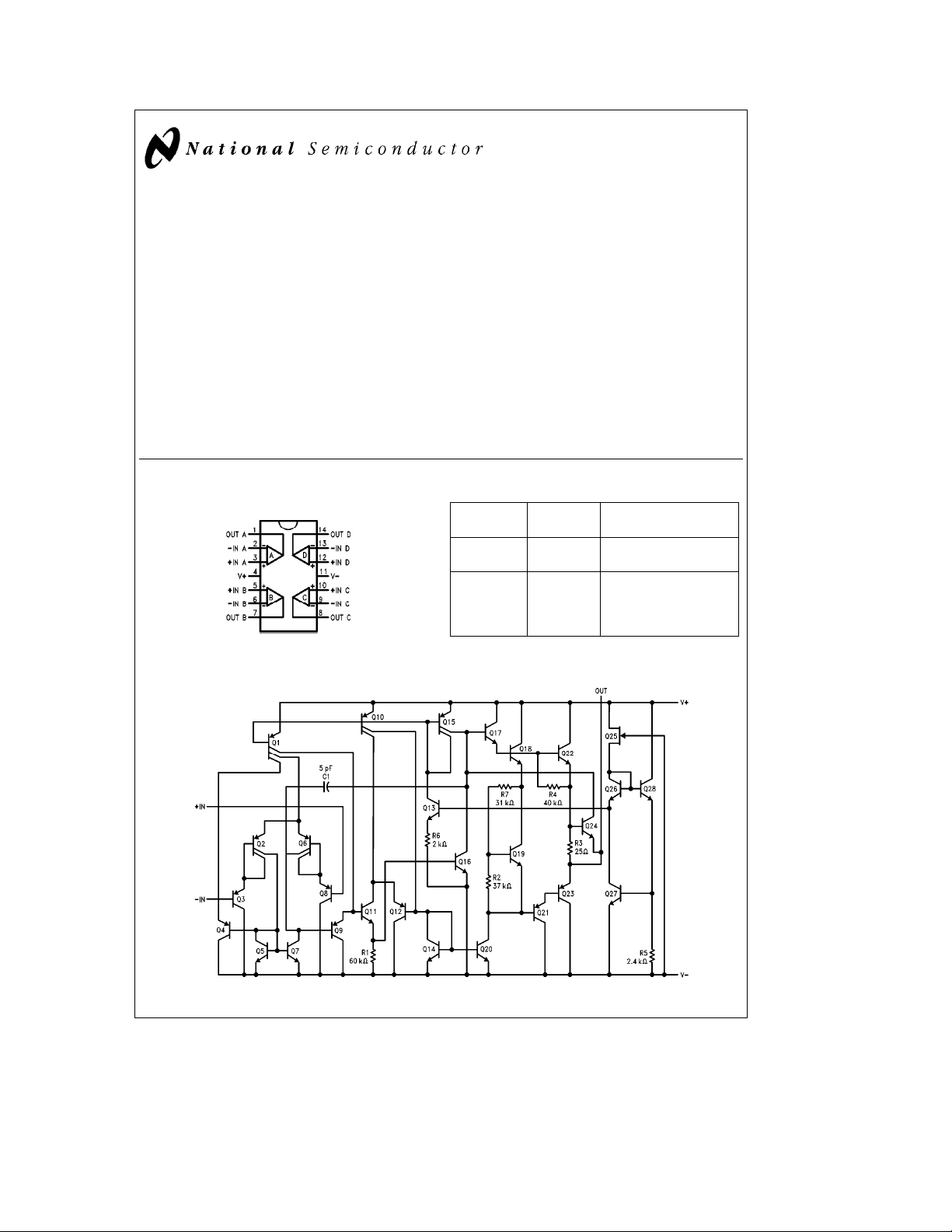
LM3303/LM3403 Quad Operational Amplifiers
Connection Diagram
14-Lead DIP and SO-14 Package
Top View
Equivalent Circuit ((/4 of Circuit)
TL/H/10064– 1
Order Information
Device Package Package
Code Code Description
LM3303J J14A Ceramic DIP
LM3303N N14A Molded DIP
LM3303M M14A Molded Surface Mount
LM3403J J14A Ceramic DIP
LM3403N N14A Molded DIP
LM3403M M14A Molded Surface Mount
TL/H/10064– 2
C
1995 National Semiconductor Corporation RRD-B30M115/Printed in U. S. A.
TL/H/10064
Page 2
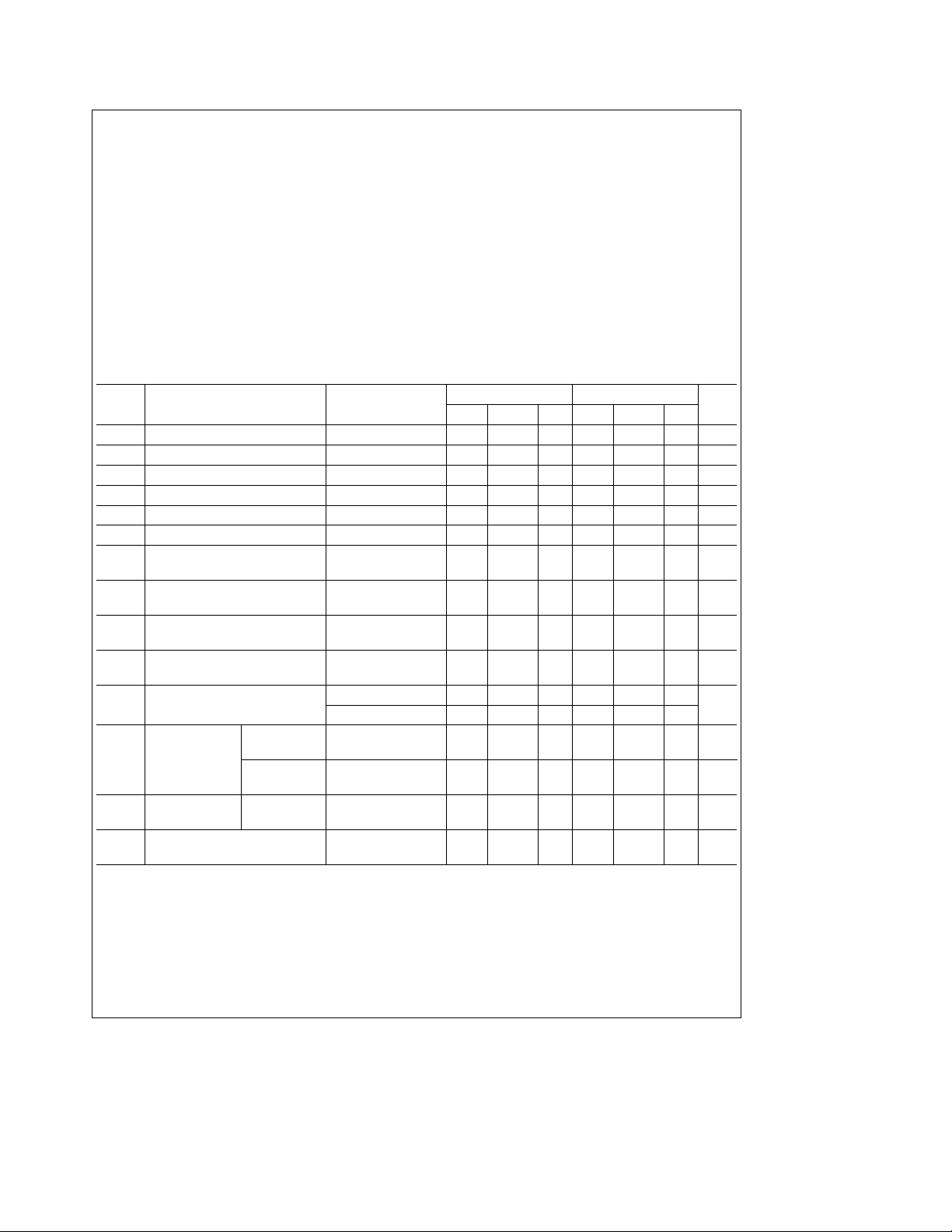
Absolute Maximum Ratings
If Military/Aerospace specified devices are required,
please contact the National Semiconductor Sales
Office/Distributors for availability and specifications.
Storage Temperature Range
Ceramic DIP
Molded DIP and SO-14
Operating Temperature Range
Industrial (LM3303)
Commercial (LM3403) 0
b
65§Ctoa175§C
b
65§Ctoa150§C
b
40§Ctoa85§C
Ctoa70§C
§
Lead Temperature
Ceramic DIP (Soldering, 60 sec.) 300
Molded DIP and SO-14
(Soldering, 10 sec.) 265
C
§
C
§
LM3303 and LM3403
Electrical Characteristics
e
T
25§C, V
A
Symbol Parameter Conditions
V
I
IO
I
IB
Z
I
CC
CMR Common Mode Rejection R
V
Input Offset Voltage 2.0 8.0 2.0 8.0 mV
IO
Input Offset Current 30 75 30 50 nA
Input Bias Current 200 500 200 500 nA
Input Impedance 0.3 1.0 0.3 1.0 MX
I
Supply Current V
Input Voltage Range
IR
e
O
s
S
PSRR Power Supply
Rejection Ratio
I
OS
A
V
TR Transient Rise Time/ V
BW Bandwidth V
SR Slew Rate V
Output Short Circuit Current
(Per Amplifier) (Note 4)
Large Signal Voltage Gain V
VS
Output Voltage Swing R
OP
Response Fall Time A
Overshoot V
R
R
A
A
A
O
t
L
e
L
e
L
O
e
V
O
e
V
O
e
V
eb
I
e
V
e
e
e
e
e
CC
e %
0V, R
L
10 kX 70 90 70 90 dB
g
10V,
2.0 kX
10 kX
2.0 kX
50 mV,
e
1.0, R
L
50 mV,
e
1.0, R
L
50 mV,
e
1.0, R
L
10V toa10V,
1.0
Internal Power Dissipation (Notes 1, 2)
14L-Ceramic DIP 1.36W
14L-Molded DIP 1.04W
SO-14 0.93W
a
Supply Voltage between V
and V
b
Differential Input Voltage (Note 3)
Input Voltage (Vb)b0.3V to V
ESD Tolerance (To Be Determined)
g
15V, unless otherwise specified
LM3303 LM3403
Min Typ Max Min Typ Max
2.8 7.0 2.8 7.0 mA
a
12Va12.5V
b
to V
to V
b
a
13Va13.5V
to Vbto V
b
30 150 30 150 mV/V
g
10
g
30g45g10
g
30g45 mA
20 200 20 200 V/mV
10 kX
10 kX
10 kX
g
12 12.5
g
10 12
0.3 0.3 ms
5.0 5.0 %
1.0 1.0 MHz
g
12a13.5
g
10
g
13
0.6 0.6 V/ms
g
36V
30V
a
Units
V
V
2
Page 3
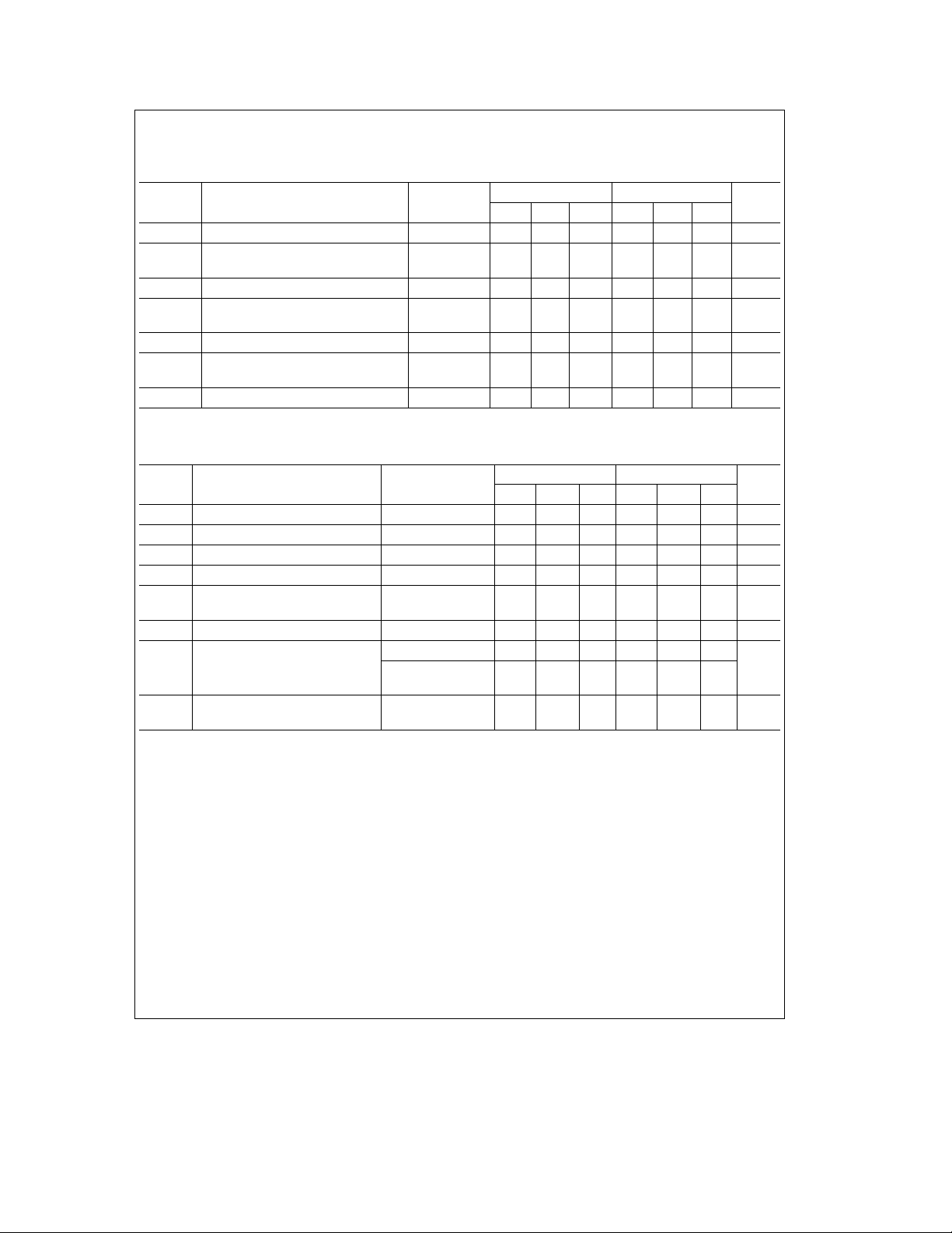
LM3303 and LM3403 (Continued)
e
Electrical Characteristics T
A
25§C, V
The following specifications apply forb40§CsT
Symbol Parameter Conditions
V
IO
Input Offset Voltage 10 10 mV
DVIO/DT Input Offset Voltage
Temperature Sensitivity
I
IO
Input Offset Current 250 200 nA
DIIO/DT Input Offset Current
Temperature Sensitivity
I
IB
A
VS
V
OP
Input Bias Current 1000 800 nA
Large Signal Voltage Gain V
Output Voltage Swing R
e
g
15V, unless otherwise specified
CC
s
a
85§C for the LM3303, and 0§CsT
A
e
O
t
R
L
e
L
g
10V,
2.0 kX
2.0 kX
LM3303 and LM3403
Electrical Characteristics
Symbol Parameter Conditions
V
IO
I
IO
I
IB
I
CC
PSRR Power Supply
A
VS
V
OP
CS Channel Separation 1.0 Hzsfs20 kHz
Note 1: T
Note 2: Ratings apply to ambient temperature at 25
the SO-14 at 7.5 mW/
Note 3: For supply voltage less than 30V between V
Note 4: Not to exceed maximum package power dissipation.
Note 5: Output will swing to ground.
Input Offset Voltage 8.0 2.0 8.0 mV
Input Offset Current 75 30 50 nA
Input Bias Current 500 200 500 nA
Supply Current 2.5 7.0 2.5 7.0 mA
Rejection Ratio
Large Signal Voltage Gain R
Output Voltage Swing R
(Note 5)
e
150§C for the Molded DIP and SO-14, and 175§C for the Ceramic DIP.
J Max
C.
§
e
T
25§C, Vae5.0V, VbeGND, unless otherwise specified
A
t
2.0 kX 20 200 20 200 V/mV
L
e
10 kX 3.3 3.3
L
s
a
5.0VsV
e
R
L
30V, (Va)(V
10 kX
(Input Referenced)
C. Above this temperature, derate the 14L-Ceramic DIP at 9.1 mW/§C, the 14L-Molded DIP at 8.3 mW/§C, and
§
a
and Vb, the absolute maximum input voltage is equal to the supply voltage.
s
a
70§C for the LM3403
A
LM3303 LM3403
Units
Min Typ Max Min Typ Max
10 10 mV/
50 50 pA/
15 15 V/mV
g
10
LM3303 LM3403
g
10 V
Units
Min Typ Max Min Typ Max
150 150 mV/V
a
b
2.0
b
120
)
b
2.0
b
120 dB
C
§
C
§
V
3
Page 4

Typical Performance Characteristics
Open Loop
Frequency Response
Output Swing vs
Supply Voltage
Sine Wave Response vs Frequency
Input Bias Current
vs Temperature
Output Voltage
Input Bias Current
vs Supply Voltage
TL/H/10064– 3
4
Page 5

Typical Applications
Multiple Feedback Bandpass Filter
Comparator with Hysteresis
e
f
center frequency
o
e
BW
Bandwidth
RinkX
CinmF
f
o
k
e
Q
10
BW
Q
eC2e
C1
3
1R3e9Q
2
b
1(Using scaling factors in these expressions.
eR2e
R1
If source impedance is high or varies, filter may be preceded with voltage
follower buffer to stabilize filter parameters.
TL/H/10064– 4
Design example:
e
Let R1
then R3
5, f
e
e
e
R3
e
C
e
1 kHz
o
R2e10 kX
2
9(5)
215 kX
5
e
1.6 nF
3
b
10
given: Q
Wein Bridge Oscillator
R1
V
V
H
IL
IH
e
e
R1aR2
e
R1aR2
R1aR2
R1
b
V
(V
R1
(V
(V
OH
)aV
OL
REF
REF
b
V
)aV
OH
REF
b
VOL)
High Impedance Differential Amplifier
e
V
C(1aaab)(V2bV1)
OUT
R2
R6
A
for best CMRR
R5
R7
e
R4
R1
e
R5
R2
R6
Gain
e
2R1
a
e
1
R5
#
R3
C(1aaab)
J
TL/H/10064– 6
REF
TL/H/10064– 7
AC Coupled Non-Inverting Amplifier
TL/H/10064– 5
1
e
f
o
2qRC
for f
e
1 kHz
o
e
R
16 kX
e
0.01 mF
C
TL/H/10064– 9
A
A
V
V
e1a
e
R2
R1
11 (as shown)
5
Page 6

Typical Applications (Continued)
AC Coupled Inverting Amplifier
Voltage Reference
e
A
V
e
A
V
Rf
R1
10 (as shown)
Ground Referencing a
Differential Input Signal
R1
e
V
O
R1aR2
1
e
a
V
V
O
TL/H/10064– 8
TL/H/10064– 11
2
Voltage Controlled Oscillator
a
V
e
2
#
as shown
J
Pulse Generator
TL/H/10064– 10
TL/H/10064– 14
Note 1: Wide Control Voltage Range:
s
s
0V
V
2(Vg1.5V)
CO
TL/H/10064– 12
6
Page 7

Typical Applications (Continued)
Function Generator
Note 2: f
e
R1aR2
4CRfR1
if R3
e
R2aR1
R2R1
BW
e
Q
f
o
where:
e
T
Center Frequency Gain
BP
e
Bandpass Notch Gain
T
N
1
e
f
,V
o
2qRC
R1eQR
R1
e
R2
T
BP
R3eTNR2
e
10 C
C1
REF
1
e
2
Bi-Quad Filter
V
CC
Example:
e
1000 Hz
f
o
e
BW
e
T
BP
e
T
N
e
160 kX
R
e
R1
e
R2
e
R3
e
0.001 mF
C
100 Hz
1
1
1.6 MX
1.6 MX
1.6 MX
TL/H/10064– 13
TL/H/10064– 15
7
Page 8

8
Page 9

Physical Dimensions inches (millimeters)
14-Lead Ceramic Dual-In-Line Package (J)
Order Number LM3303J or LM3403J
NS Package Number J14A
14-Lead Molded Surface Mount (M)
Order Number LM3403M
NS Package Number M14A
9
Page 10

Physical Dimensions inches (millimeters) (Continued)
LM3303/LM3403 Quad Operational Amplifiers
Order Number LM3303N or LM3403N
NS Package Number N14A
LIFE SUPPORT POLICY
NATIONAL’S PRODUCTS ARE NOT AUTHORIZED FOR USE AS CRITICAL COMPONENTS IN LIFE SUPPORT
DEVICES OR SYSTEMS WITHOUT THE EXPRESS WRITTEN APPROVAL OF THE PRESIDENT OF NATIONAL
SEMICONDUCTOR CORPORATION. As used herein:
1. Life support devices or systems are devices or 2. A critical component is any component of a life
systems which, (a) are intended for surgical implant support device or system whose failure to perform can
into the body, or (b) support or sustain life, and whose be reasonably expected to cause the failure of the life
failure to perform, when properly used in accordance support device or system, or to affect its safety or
with instructions for use provided in the labeling, can effectiveness.
be reasonably expected to result in a significant injury
to the user.
National Semiconductor National Semiconductor National Semiconductor National Semiconductor
14-Lead Molded Dual-In-Line Package (N)
Corporation Europe Hong Kong Ltd. Japan Ltd.
1111 West Bardin Road Fax: (
Arlington, TX 76017 Email: cnjwge@tevm2.nsc.com Ocean Centre, 5 Canton Rd. Fax: 81-043-299-2408
Tel: 1(800) 272-9959 Deutsch Tel: (
Fax: 1(800) 737-7018 English Tel: (
National does not assume any responsibility for use of any circuitry described, no circuit patent licenses are implied and National reserves the right at any time without notice to change said circuitry and specifications.
Fran3ais Tel: (
Italiano Tel: (
a
49) 0-180-530 85 86 13th Floor, Straight Block, Tel: 81-043-299-2309
a
49) 0-180-530 85 85 Tsimshatsui, Kowloon
a
49) 0-180-532 78 32 Hong Kong
a
49) 0-180-532 93 58 Tel: (852) 2737-1600
a
49) 0-180-534 16 80 Fax: (852) 2736-9960
 Loading...