

Page 1
LM340/LM78XX Series
3-Terminal Positive Regulators
General Description
The LM140/LM340A/LM340/LM7800C monolithic 3-terminal
positive voltage regulators employ internal current-limiting,
thermal shutdown and safe-area compensation, making
them essentially indestructible. If adequate heat sinking is
provided, theycan deliver over 1.0A output current. They are
intended as fixed voltage regulators in a wide range of
applications including local (on-card) regulation for elimination of noise and distribution problems associated with
single-point regulation. In addition to use as fixed voltage
regulators, these devices can be used with external components to obtain adjustable output voltages and currents.
Considerable effort was expended to make the entire series
of regulators easy to use and minimize the number of external components. It is not necessary to bypass the output,
although this does improve transient response. Input bypassing is needed only if the regulator is located far from the
filter capacitor of the power supply.
The 5V, 12V, and 15V regulator options are available in the
steel TO-3 power package. The LM340A/LM340/LM7800C
series is available in the TO-220 plastic power package, and
the LM340-5.0 is available in the SOT-223 package, as well
as the LM340-5.0 and LM340-12 in the surface-mount
TO-263 package.
Features
n Complete specifications at 1A load
n Output voltage tolerances of
±
2% at Tj= 25˚C and±4%
over the temperature range (LM340A)
n Line regulation of 0.01% of V
OUT
/V of ∆VINat 1A load
(LM340A)
n Load regulation of 0.3% of V
OUT
/A (LM340A)
n Internal thermal overload protection
n Internal short-circuit current limit
n Output transistor safe area protection
n P
+
Product Enhancement tested
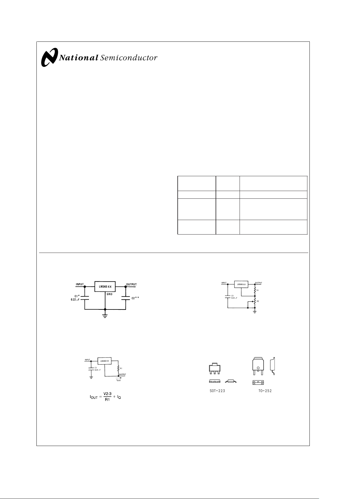
Device
Output
Voltages
Packages
LM140 5, 12, 15 TO-3 (K)
LM340A/LM340 5, 12, 15 TO-3 (K), TO-220 (T),
SOT-223 (MP), TO-263 (S)
(5V and 12V only)
LM7800C 5, 8, 12,15TO-220 (T)
Typical Applications
Fixed Output Regulator Adjustable Output Regulator
00778101
*
Required if the regulator is located far from the power supply filter.
**
Although no output capacitor is needed for stability, it does help transient
response. (If needed, use 0.1 µF, ceramic disc).
00778102
V
OUT
= 5V + (5V/R1 + IQ) R2 5V/R1>3IQ,
load regulation (L
r
) ≈ [(R1 + R2)/R1] (Lrof LM340-5).
Current Regulator
Comparison between SOT-223 and D-Pak (TO-252)
Packages
00778103
∆IQ= 1.3 mA over line and load changes.
00778138
Scale 1:1
September 2001
LM340/LM78XX Series 3-Terminal Positive Regulators
© 2001 National Semiconductor Corporation DS007781 www.national.com
Page 2
Absolute Maximum Ratings (Note 1)
If Military/Aerospace specified devices are required,
please contact the National Semiconductor Sales Office/
Distributors for availability and specifications.
(Note 5)
DC Input Voltage
All Devices except
LM7824/LM7824C 35V
LM7824/LM7824C 40V
Internal Power Dissipation (Note 2) Internally Limited
Maximum Junction Temperature 150˚C
Storage Temperature Range −65˚C to +150˚C
Lead Temperature (Soldering, 10 sec.)
TO-3 Package (K) 300˚C
TO-220 Package (T), TO-263
Package (S) 230˚C
ESD Susceptibility (Note 3) 2 kV
Operating Conditions (Note 1)
Temperature Range (T
A
) (Note 2)
LM140A, LM140 −55˚C to +125˚C
LM340A, LM340, LM7805C,
LM7812C, LM7815C, LM7808C 0˚C to +125˚C
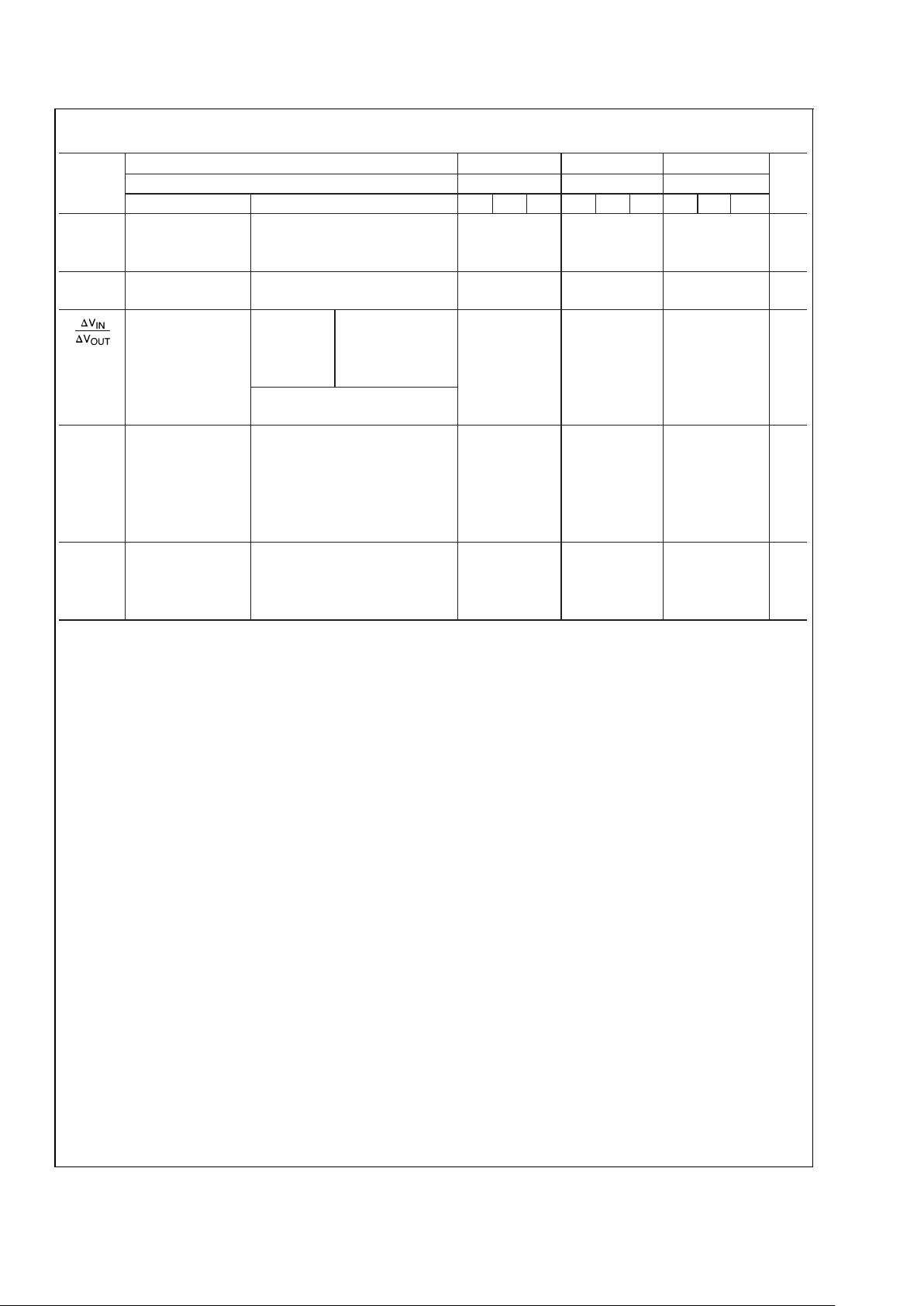
LM340A Electrical Characteristics
I
OUT
= 1A, −55˚C ≤ TJ≤ +150˚C (LM140A), or 0˚C ≤ TJ≤ + 125˚C (LM340A) unless otherwise specified (Note 4)
Output Voltage 5V 12V 15V
Symbol Input Voltage (unless otherwise noted) 10V 19V 23V Units
Parameter Conditions Min Typ Max Min Typ Max Min Typ Max
V
O
Output Voltage TJ= 25˚C 4.9 5 5.1 11.75 12 12.25 14.7 15 15.3 V
P
D
≤ 15W, 5 mA ≤ IO≤ 1A 4.8 5.2 11.5 12.5 14.4 15.6 V
V
MIN
≤ VIN≤ V
MAX
(7.5 ≤ VIN≤ 20) (14.8 ≤ VIN≤ 27) (17.9 ≤ VIN≤ 30) V
∆V
O
Line Regulation IO= 500 mA 10 18 22 mV
∆V
IN
(7.5 ≤ VIN≤ 20) (14.8 ≤ VIN≤ 27) (17.9 ≤ VIN≤ 30) V
T
J
= 25˚C 3 10 4 18 4 22 mV
∆V
IN
(7.5 ≤ VIN≤ 20) (14.5 ≤ VIN≤ 27) (17.5 ≤ VIN≤ 30) V
T
J
= 25˚C 4 9 10 mV
Over Temperature 12 30 30 mV
∆V
IN
(8 ≤ VIN≤ 12) (16 ≤ VIN≤ 22) (20 ≤ VIN≤ 26) V
∆V
O
Load Regulation TJ= 25˚C 5 mA ≤ IO≤ 1.5A 10 25 12 32 12 35 mV
250 mA ≤ I
O
≤ 750
mA
15 19 21 mV
Over Temperature, 25 60 75 mV
5mA≤I
O
≤1A
I
Q
Quiescent
Current
TJ= 25˚C 6 6 6 mA
Over Temperature 6.5 6.5 6.5 mA
∆I
Q
Quiescent
Current
5mA≤IO≤1A 0.5 0.5 0.5 mA
Change T
J
= 25˚C, IO= 1A 0.8 0.8 0.8 mA
V
MIN
≤ VIN≤ V
MAX
(7.5 ≤ VIN≤ 20) (14.8 ≤ VIN≤ 27) (17.9 ≤ VIN≤ 30) V
I
O
= 500 mA 0.8 0.8 0.8 mA
V
MIN
≤ VIN≤ V
MAX
(8 ≤ VIN≤ 25) (15 ≤ VIN≤ 30) (17.9 ≤ VIN≤ 30) V
V
N
Output Noise
Voltage
TA= 25˚C, 10 Hz ≤ f ≤ 100 kHz 40 75 90 µV
Ripple Rejection TJ= 25˚C, f = 120 Hz, IO=1A688061726070dB
or f = 120 Hz, I
O
= 500 mA, 68 61 60 dB
Over Temperature,
V
MIN
≤ VIN≤ V
MAX
(8 ≤ VIN≤ 18) (15 ≤ VIN≤ 25) (18.5 ≤ VIN≤
28.5)
V
R
O
Dropout Voltage TJ= 25˚C, IO= 1A 2.0 2.0 2.0 V
Output
Resistance
f=1kHz 8 18 19 mΩ
LM340/LM78XX
www.national.com 2
Page 3
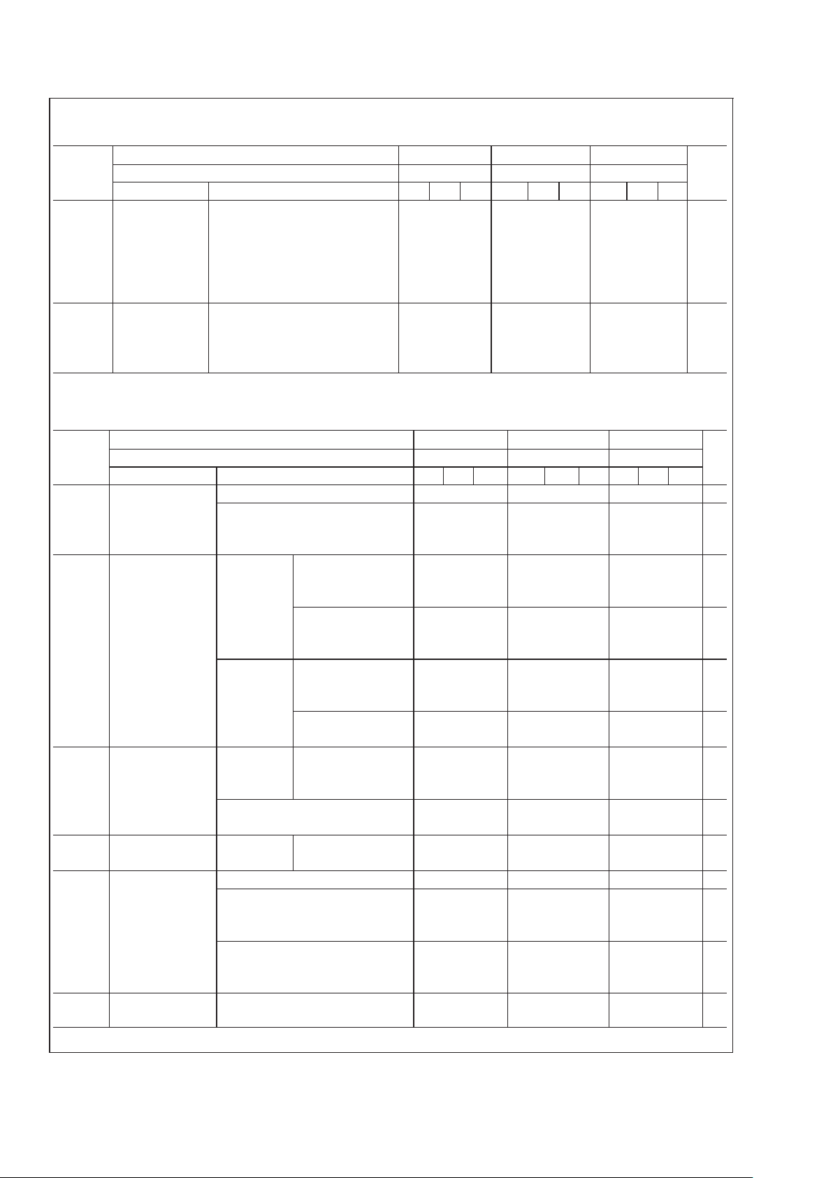
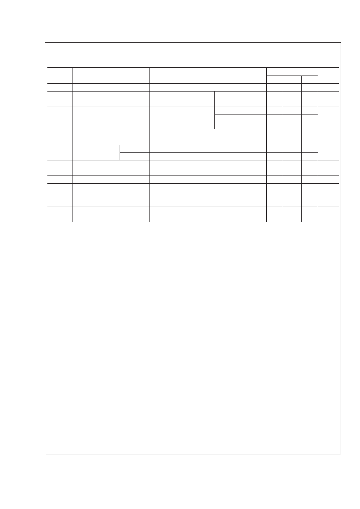
LM340A Electrical Characteristics (Continued)
I
OUT
= 1A, −55˚C ≤ TJ≤ +150˚C (LM140A), or 0˚C ≤ TJ≤ + 125˚C (LM340A) unless otherwise specified (Note 4)
Output Voltage 5V 12V 15V
Symbol Input Voltage (unless otherwise noted) 10V 19V 23V Units
Parameter Conditions Min Typ Max Min Typ Max Min Typ Max
Short-Circuit
Current
T
J
= 25˚C 2.1 1.5 1.2 A
Peak Output
Current
T
J
= 25˚C 2.4 2.4 2.4 A
Average TC of
V
O
Min, TJ= 0˚C, IO= 5 mA −0.6 −1.5 −1.8 mV/˚C
V
IN
Input Voltage TJ= 25˚C
Required to
Maintain
7.5 14.5 17.5 V
Line Regulation
LM140 Electrical Characteristics (Note 4)
−55˚C ≤ TJ≤ +150˚C unless otherwise specified
Output Voltage 5V 12V 15V
Symbol Input Voltage (unless otherwise noted) 10V 19V 23V Units
Parameter Conditions Min Typ Max Min Typ Max Min Typ Max
V
O
Output Voltage TJ= 25˚C, 5 mA ≤ IO≤ 1A 4.8 5 5.2 11.5 12 12.5 14.4 15 15.6 V
P
D
≤ 15W, 5 mA ≤ IO≤ 1A 4.75 5.25 11.4 12.614.25 15.75 V
V
MIN
≤ VIN≤ V
MAX
(8 ≤ VIN≤ 20) (15.5 ≤ VIN≤ 27) (18.5 ≤ VIN≤
30)
V
∆V
O
Line Regulation IO= 500 mA TJ= 25˚C 3 50 4 120 4 150 mV
∆V
IN
(7 ≤ VIN≤ 25) (14.5 ≤ VIN≤ 30) (17.5 ≤ VIN≤
30)
V
−55˚C ≤ T
J
≤ +150˚C 50 120 150 mV
∆V
IN
(8 ≤ VIN≤ 20) (15 ≤ VIN≤ 27) (18.5 ≤ VIN≤
30)
V
I
O
≤ 1A TJ= 25˚C 50 120 150 mV
∆V
IN
(7.5 ≤ VIN≤ 20) (14.6 ≤ VIN≤ 27) (17.7 ≤ VIN≤
30)
V
−55˚C ≤ T
J
≤ +150˚C 25 60 75 mV
∆V
IN
(8 ≤ VIN≤ 12) (16 ≤ VIN≤ 22) (20 ≤ VIN≤ 26) V
∆V
O
Load Regulation TJ= 25˚C 5 mA ≤ IO≤ 1.5A 10 50 12 120 12 150 mV
250 mA ≤ I
P
≤ 750
mA
25 60 75 mV
−55˚C ≤ T
J
≤ +150˚C, 50 120 150 mV
5mA≤I
O
≤1A
I
Q
Quiescent Current IO≤ 1A TJ= 25˚C 6 6 6 mA
−55˚C ≤ T
J
≤ +150˚C 7 7 7 mA
∆I
Q
Quiescent Current 5 mA ≤ IO≤ 1A 0.5 0.5 0.5 mA
Change T
J
= 25˚C, IO≤ 1A 0.8 0.8 0.8 mA
V
MIN
≤ VIN≤ V
MAX
(8 ≤ VIN≤ 20) (15 ≤ VIN≤ 27) (18.5 ≤ VIN≤
30)
V
I
O
= 500 mA, −55˚C ≤ TJ≤ +150˚C 0.8 0.8 0.8 mA
V
MIN
≤ VIN≤ V
MAX
(8 ≤ VIN≤ 25) (15 ≤ VIN≤ 30) (18.5 ≤ VIN≤
30)
V
V
N
Output Noise
Voltage
TA= 25˚C, 10 Hz ≤ f ≤ 100 kHz 40 75 90 µV
LM340/LM78XX
www.national.com3
Page 4
LM140 Electrical Characteristics (Note 4) (Continued)
−55˚C ≤ TJ≤ +150˚C unless otherwise specified
Output Voltage 5V 12V 15V
Symbol Input Voltage (unless otherwise noted) 10V 19V 23V Units
Parameter Conditions Min Typ Max Min Typ Max Min Typ Max
Ripple Rejection IO≤ 1A, TJ= 25˚Cor68 80 61 72 60 70 dB
f = 120 Hz I
O
≤ 500 mA, 68 61 60 dB
−55˚C ≤ T
J
≤+150˚C
V
MIN
≤ VIN≤ V
MAX
(8 ≤ VIN≤ 18) (15 ≤ VIN≤ 25) (18.5 ≤ VIN≤
28.5)
V
R
O
Dropout Voltage TJ= 25˚C, IO= 1A 2.0 2.0 2.0 V
Output Resistance f = 1 kHz 8 18 19 mΩ
Short-Circuit
Current
T
J
= 25˚C 2.1 1.5 1.2 A
Peak Output
Current
T
J
= 25˚C 2.4 2.4 2.4 A
Average TC of
V
OUT
0˚C ≤ TJ≤ +150˚C, IO= 5 mA −0.6 −1.5 −1.8 mV/˚C
V
IN
Input Voltage TJ= 25˚C, IO≤ 1A
Required to
Maintain
7.5 14.6 17.7 V
Line Regulation
LM340/LM7800C Electrical Characteristics (Note 4)
0˚C ≤ TJ≤ +125˚C unless otherwise specified
Output Voltage 5V 12V 15V
Symbol Input Voltage (unless otherwise noted) 10V 19V 23V Units
Parameter Conditions Min Typ Max Min Typ Max Min Typ Max
V
O
Output Voltage TJ= 25˚C, 5 mA ≤ IO≤ 1A 4.8 5 5.2 11.5 12 12.5 14.4 15 15.6 V
P
D
≤ 15W, 5 mA ≤ IO≤ 1A 4.75 5.25 11.4 12.6 14.25 15.75 V
V
MIN
≤ VIN≤ V
MAX
(7.5 ≤ VIN≤ 20) (14.5 ≤ VIN≤
27)
(17.5 ≤ VIN≤ 30) V
∆V
O
Line Regulation IO= 500 mA TJ= 25˚C 3 50 4 120 4 150 mV
∆V
IN
(7 ≤ VIN≤ 25) (14.5 ≤ VIN≤
30)
(17.5 ≤ VIN≤ 30) V
0˚C ≤ T
J
≤ +125˚C 50 120 150 mV
∆V
IN
(8 ≤ VIN≤ 20) (15 ≤ VIN≤ 27) (18.5 ≤ VIN≤ 30) V
I
O
≤ 1A TJ= 25˚C 50 120 150 mV
∆V
IN
(7.5 ≤ VIN≤ 20) (14.6 ≤ VIN≤
27)
(17.7 ≤ VIN≤ 30) V
0˚C ≤ T
J
≤ +125˚C 25 60 75 mV
∆V
IN
(8 ≤ VIN≤ 12) (16 ≤ VIN≤ 22) (20 ≤ VIN≤ 26) V
∆V
O
Load Regulation TJ= 25˚C 5 mA ≤ IO≤ 1.5A 10 50 12 120 12 150 mV
250 mA ≤ I
O
≤ 750 mA 25 60 75 mV
5mA≤I
O
≤1A, 0˚C ≤ TJ≤
+125˚C
50 120 150 mV
I
Q
Quiescent Current IO≤ 1A TJ= 25˚C 8 8 8 mA
0˚C ≤ T
J
≤ +125˚C 8.5 8.5 8.5 mA
∆I
Q
Quiescent Current 5 mA ≤ IO≤ 1A 0.5 0.5 0.5 mA
Change T
J
= 25˚C, IO≤ 1A 1.0 1.0 1.0 mA
V
MIN
≤ VIN≤ V
MAX
(7.5 ≤ VIN≤ 20) (14.8 ≤ VIN≤
27)
(17.9 ≤ VIN≤ 30) V
LM340/LM78XX
www.national.com 4
Page 5
LM340/LM7800C Electrical Characteristics (Note 4) (Continued)
0˚C ≤ TJ≤ +125˚C unless otherwise specified
Output Voltage 5V 12V 15V
Symbol Input Voltage (unless otherwise noted) 10V 19V 23V Units
Parameter Conditions Min Typ Max Min Typ Max Min Typ Max
I
O
≤ 500 mA, 0˚C ≤ TJ≤ +125˚C 1.0 1.0 1.0 mA
V
MIN
≤ VIN≤ V
MAX
(7 ≤ VIN≤ 25) (14.5 ≤ VIN≤
30)
(17.5 ≤ VIN≤ 30) V
V
N
Output Noise
Voltage
TA= 25˚C, 10 Hz ≤ f ≤ 100 kHz 40 75 90 µV
Ripple Rejection IO≤ 1A, TJ=
25˚C
62 80 55 72 54 70 dB
f = 120 Hz or I
O
≤ 500 mA, 62 55 54 dB
0˚C ≤ T
J
≤ +125˚C
V
MIN
≤ VIN≤ V
MAX
(8 ≤ VIN≤ 18) (15 ≤ VIN≤ 25) (18.5 ≤ VIN≤
28.5)
V
R
O
Dropout Voltage TJ= 25˚C, IO= 1A 2.0 2.0 2.0 V
Output Resistance f = 1 kHz 8 18 19 mΩ
Short-Circuit Current T
J
= 25˚C 2.1 1.5 1.2 A
Peak Output
Current
T
J
= 25˚C 2.4 2.4 2.4 A
Average TC of V
OUT
0˚C ≤ TJ≤ +125˚C, IO= 5 mA −0.6 −1.5 −1.8 mV/˚C
V
IN
Input Voltage TJ= 25˚C, IO≤ 1A
Required to
Maintain
7.5 14.6 17.7 V
Line Regulation
Note 1: Absolute Maximum Ratings are limits beyond which damage to the device may occur. Operating Conditions are conditions under which the device functions
but the specifications might not be guaranteed. For guaranteed specifications and test conditions see the Electrical Characteristics.
Note 2: The maximum allowable power dissipation at any ambient temperature is a function of the maximum junction temperature for operation (T
JMAX
= 125˚C
or 150˚C), the junction-to-ambient thermal resistance (θ
JA
), and the ambient temperature (TA). P
DMAX
=(T
JMAX−TA
)/θJA. If this dissipation is exceeded, the die
temperature will rise above T
JMAX
and the electrical specifications do not apply. If the die temperature rises above 150˚C, the device will go into thermal shutdown.
For the TO-3 package (K, KC), the junction-to-ambient thermal resistance (θ
JA
) is 39˚C/W. When using a heatsink, θJAis the sum of the 4˚C/W junction-to-case
thermal resistance (θ
JC
) of the TO-3 package and the case-to-ambient thermal resistance of the heatsink. For the TO-220 package (T), θJAis 54˚C/W and θJCis
4˚C/W. If SOT-223 is used, the junction-to-ambient thermal resistance is 174˚C/W and can be reduced by a heatsink (see Applications Hints on heatsinking).
If theTO-263 package is used, the thermal resistance can be reduced by increasing the PC board copper area thermally connected to the package: Using 0.5 square
inches of copper area, θ
JA
is 50˚C/W; with 1 square inch of copper area, θJAis 37˚C/W; and with 1.6 or more inches of copper area, θJAis 32˚C/W.
Note 3: ESD rating is based on the human body model, 100 pF discharged through 1.5 kΩ.
Note 4: All characteristics are measured with a 0.22 µF capacitor from input to ground and a 0.1 µF capacitor from output to ground.All characteristics except noise
voltage and ripple rejection ratio are measured using pulse techniques (t
w
≤ 10 ms, duty cycle ≤ 5%). Output voltage changes due to changes in internal temperature
must be taken into account separately.
Note 5: A military RETS specification is available on request. At the time of printing, the military RETS specifications for the LM140AK-5.0/883, LM140AK-12/883,
and LM140AK-15/883 complied with the min and max limits for the respective versions of the LM140A. At the time of printing, the military RETS specifications for
the LM140K-5.0/883, LM140K-12/883, and LM140K-15/883 complied with the min and max limits for the respective versions of the LM140. The LM140H/883,
LM140K/883, and LM140AK/883 may also be procured as a Standard Military Drawing.
LM340/LM78XX
www.national.com5
Page 6
LM7808C
Electrical Characteristics
0˚C ≤ TJ≤ +150˚C, VI= 14V, IO= 500 mA, CI= 0.33 µF, CO= 0.1 µF, unless otherwise specified
Symbol Parameter Conditions (Note 6) LM7808C Units
Min Typ Max
V
O
Output Voltage TJ= 25˚C 7.7 8.0 8.3 V
∆V
O
Line Regulation TJ= 25˚C 10.5V ≤ VI≤ 25V 6.0 160 mV
11.0V ≤ V
I
≤ 17V 2.0 80
∆V
O
Load Regulation TJ= 25˚C 5.0 mA ≤ IO≤ 1.5A 12 160 mV
250 mA ≤ I
O
≤ 750
mA
4.0 80
V
O
Output Voltage 11.5V ≤ VI≤ 23V, 5.0 mA ≤ IO≤ 1.0A, P ≤ 15W 7.6 8.4 V
I
Q
Quiescent Current TJ= 25˚C 4.3 8.0 mA
∆I
Q
Quiescent With Line 11.5V ≤ VI≤ 25V 1.0 mA
Current Change With Load 5.0 mA ≤ I
O
≤ 1.0A 0.5
V
N
Noise TA= 25˚C, 10 Hz ≤ f ≤ 100 kHz 52 µV
∆V
I
/∆VORipple Rejection f = 120 Hz, IO= 350 mA, TJ= 25˚C 56 72 dB
V
DO
Dropout Voltage IO= 1.0A, TJ= 25˚C 2.0 V
R
O
Output Resistance f = 1.0 kHz 16 mΩ
I
OS
Output Short Circuit Current TJ= 25˚C, VI= 35V 0.45 A
I
PK
Peak Output Current TJ= 25˚C 2.2 A
∆V
O
/∆T Average Temperature IO= 5.0 mA 0.8 mV/˚C
Coefficient of Output Voltage
Note 6: All characteristics are measured with a 0.22 µF capacitor from input to ground and a 0.1 µF capacitor from output to ground.All characteristics except noise
voltage and ripple rejection ratio are measured using pulse techniques (t
w
≤ 10 ms, duty cycle ≤ 5%). Output voltage changes due to changes in internal temperature
must be taken into account separately.
LM340/LM78XX
www.national.com 6
Page 7

Typical Performance
Characteristics
Maximum Average Power Dissipation Maximum Average Power Dissipation
00778122 00778123
Maximum Power Dissipation (TO-263)
(See Note 2) Output Voltage (Normalized to 1V at T
J
= 25˚C)
00778124 00778125
Note: Shaded area refers to LM340A/LM340, LM7805C, LM7812C and
LM7815C.
Ripple Rejection Ripple Rejection
00778126
00778127
LM340/LM78XX
www.national.com7
Page 8

Typical Performance Characteristics (Continued)
Output Impedance Dropout Characteristics
00778128
00778129
Quiescent Current Peak Output Current
00778130
Note: Shaded area refers to LM340A/LM340, LM7805C, LM7812C and
LM7815C.
00778131
Dropout Voltage Quiescent Current
00778132
Note: Shaded area refers to LM340A/LM340, LM7805C, LM7812C and
LM7815C.
00778133
LM340/LM78XX
www.national.com 8
Page 9

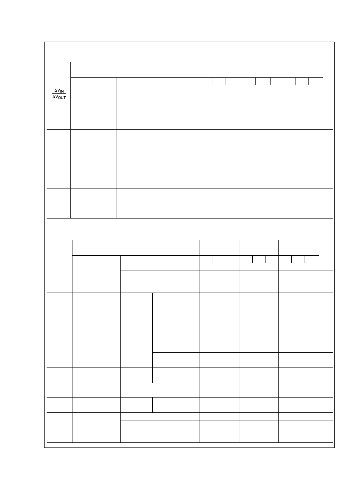
Line Regulation
140AK-5.0, I
OUT
= 1A, TA= 25˚C
Line Regulation
140AK-5.0, VIN= 10V, TA= 25˚C
00778105
00778106
Equivalent Schematic
00778107
Application Hints
The LM340/LM78XX series is designed with thermal protection, output short-circuit protection and output transistor safe
area protection. However, as with
any
IC regulator, it becomes necessary to take precautions to assure that the
regulator is not inadvertently damaged. The following describes possible misapplications and methods to prevent
damage to the regulator.
Shorting the Regulator Input: When using large capacitors
at the output of these regulators, a protection diode connected input to output (
Figure 1
) may be required if the input
is shorted to ground. Without the protection diode, an input
short will cause the input to rapidly approach ground poten-
tial, while the output remains near the initial V
OUT
because of
the stored charge in the large output capacitor. The capacitor
will then discharge through a large internal input to output
diode and parasitic transistors. If the energy released by the
capacitor is large enough, this diode, low current metal and
the regulator will be destroyed. The fast diode in
Figure 1
will
shunt most of the capacitors discharge current around the
regulator. Generally no protection diode is required for values of output capacitance ≤ 10 µF.
Raising the Output Voltage above the Input Voltage:
Since the output of the device does not sink current, forcing
the output high can cause damage to internal low current
paths in a manner similar to that just described in the “Shorting the Regulator Input” section.
LM340/LM78XX
www.national.com9
Page 10

Application Hints (Continued)
Regulator Floating Ground (
Figure 2
): When the ground
pin alone becomes disconnected, the output approaches the
unregulated input, causing possible damage to other circuits
connected to V
OUT
. If ground is reconnected with power
“ON”, damage may also occur to the regulator. This fault is
most likely to occur when plugging in regulators or modules
with on card regulators into powered up sockets. Power
should be turned off first, thermal limit ceases operating, or
ground should be connected first if power must be left on.
Transient Voltages: If transients exceed the maximum
rated input voltage of the device, or reach more than 0.8V
below ground and have sufficient energy, they will damage
the regulator. The solution is to use a large input capacitor, a
series input breakdown diode, a choke, a transient suppressor or a combination of these.
When a value for θ
(H–A)
is found using the equation shown,
a heatsink must be selected that has
a value that is less than
or equal to this number.
θ
(H–A)
is specified numerically by the heatsink manufacturer
in this catalog, or shown in a curve that plots temperature
rise vs power dissipation for the heatsink.
HEATSINKING TO-263 AND SOT-223 PACKAGE PARTS
Both the TO-263 (“S”) and SOT-223 (“MP”) packages use a
copper plane on the PCB and the PCB itself as a heatsink.
To optimize the heat sinking ability of the plane and PCB,
solder the tab of the plane.
shows for the TO-263 the measured values of θ
(J–A)
for
different copper area sizes using a typical PCB with 1 ounce
copper
and no solder mask over the copper area used for
heatsinking
.
As shown in the figure, increasing the copper area beyond 1
square inch produces very little improvement. It should also
be observed that the minimum value of θ
(J–A)
for the TO-263
package mounted to a PCB is 32˚C/W.
As a design aid,
Figure 5
shows the maximum allowable
power dissipation compared to ambient temperature for the
TO-263 device (assuming θ
(J–A)
is 35˚C/W and the maxi-
mum junction temperature is 125˚C).
00778108
FIGURE 1. Input Short
00778109
FIGURE 2. Regulator Floating Ground
00778110
FIGURE 3. Transients
00778139
FIGURE 4. θ
(J–A)
vs Copper (1 ounce)
Area for the TO-263 Package
LM340/LM78XX
www.national.com 10
Page 11

Application Hints (Continued)
Figures 6, 7
show the information for the SOT-223 package.
Figure 6
assumes a θ
(J–A)
of 74˚C/W for 1 ounce copper and
51˚C/W for 2 ounce copper and a maximum junction temperature of 125˚C.
Please see AN-1028 for power enhancement techniques to
be used with the SOT-223 package.
Typical Applications
Fixed Output Regulator
00778113
Note: Bypass capacitors are recommended for optimum stability and transient response, and should be located as close as possible to the regulator.
High Input Voltage Circuits
00778114
00778140
FIGURE 5. Maximum Power Dissipation vs
T
AMB
for the TO-263 Package
00778141
FIGURE 6. θ
(J–A)
vs Copper (2 ounce) Area
for the SOT-223 Package
00778142
FIGURE 7. Maximum Power Dissipation vs
T
AMB
for the SOT-223 Package
LM340/LM78XX
www.national.com11
Page 12

Typical Applications (Continued)
00778115
High Current Voltage Regulator
00778116
High Output Current, Short Circuit Protected
00778117
LM340/LM78XX
www.national.com 12
Page 13

Typical Applications (Continued)
Positive and Negative Regulator
00778118
Connection Diagrams and
Ordering Information
TO-3 Metal Can Package (K)
00778111
Bottom View
Steel Package Order Numbers:
LM140K-5.0 LM140K-12 LM140K-15
LM340K-12 LM340K-15
LM340K-5.0
See Package Number K02A
LM140K-5.0/883 LM140K-12/883 LM140K-15/883
See Package Number K02C
TO-220 Power Package (T)
00778112
Top View
Plastic Package Order Numbers:
LM340AT-5.0 LM340T-5.0
LM340T-12 LM340T-15
LM7805CT LM7812CT
LM7815CT LM7808CT
See Package Number T03B
TO-39 Metal Can Package (H)
00778119
Top View
Metal Can Order Numbers
†
:
LM140H-5.0/883 LM140H-6.0/883
LM140H-8.0/883 LM140H-12/883
LM140H-15/883 LM140H-24/883
See Package Number H03A
LM340/LM78XX
www.national.com13
Page 14

Connection Diagrams and
Ordering Information
(Continued)
TO-263 Surface-Mount Package (S)
00778120
Top View
00778121
Side View
Surface-Mount Package Order Numbers:
LM340S-5.0 LM340S-12
See Package Number TS3B
3-Lead SOT-223
(Front View)
Order Number LM340MP-5.0
Package Marked NO0A
See Package Number MA04A
00778143
†
The specifications for the LM140H/883 devices are not contained in this datasheet. If specifications for these devices
are required, contact the National Semiconductor Sales Office/Distributors.
LM340/LM78XX
www.national.com 14
Page 15

Physical Dimensions inches (millimeters)
unless otherwise noted
TO-3 Metal Can Package (K)
Order Number LM140K-5.0, LM340K-5.0, LM140K-12, LM340K-12,
LM140K-15, LM340K-15, LM7806CK, LM7808CK, LM7818CK or LM7824CK
NS Package Number K02A
TO-3 Metal Can Package (K)
Mil-Aero Products
Order Number LM140K-5.0/883, LM140K-12/883, or LM140K-15/883
NS Package Number K02C
LM340/LM78XX
www.national.com15
Page 16

Physical Dimensions inches (millimeters) unless otherwise noted (Continued)
TO-263 Surface-Mount Package (S)
Order Number LM340S-5.0 or LM340S-12
NS Package Number TS3B
LM340/LM78XX
www.national.com 16
Page 17

Physical Dimensions inches (millimeters) unless otherwise noted (Continued)
TO-220 Power Package (T)
Order Number LM340AT/LM340T-5.0, LM340AT/LM340T-12, LM340AT/LM340T-15,
LM7805CT, LM7812CT, LM7815CT, LM7806CT, LM7808CT, LM7818CT or LM7824CT
NS Package Number T03B
LM340/LM78XX
www.national.com17
Page 18

Physical Dimensions inches (millimeters) unless otherwise noted (Continued)
3-Lead SOT-223 Package
Order Part Number LM340MP-5.0
NS Package Number MA04A
LIFE SUPPORT POLICY
NATIONAL’S PRODUCTS ARE NOT AUTHORIZED FOR USE AS CRITICAL COMPONENTS IN LIFE SUPPORT
DEVICES OR SYSTEMS WITHOUT THE EXPRESS WRITTEN APPROVAL OF THE PRESIDENT AND GENERAL
COUNSEL OF NATIONAL SEMICONDUCTOR CORPORATION. As used herein:
1. Life support devices or systems are devices or
systems which, (a) are intended for surgical implant
into the body, or (b) support or sustain life, and
whose failure to perform when properly used in
accordance with instructions for use provided in the
labeling, can be reasonably expected to result in a
significant injury to the user.
2. A critical component is any component of a life
support device or system whose failure to perform
can be reasonably expected to cause the failure of
the life support device or system, or to affect its
safety or effectiveness.
National Semiconductor
Corporation
Americas
Email: support@nsc.com
National Semiconductor
Europe
Fax: +49 (0) 180-530 85 86
Email: europe.support@nsc.com
Deutsch Tel: +49 (0) 69 9508 6208
English Tel: +44 (0) 870 24 0 2171
Français Tel: +33 (0) 1 41 91 8790
National Semiconductor
Asia Pacific Customer
Response Group
Tel: 65-2544466
Fax: 65-2504466
Email: ap.support@nsc.com
National Semiconductor
Japan Ltd.
Tel: 81-3-5639-7560
Fax: 81-3-5639-7507
www.national.com
LM340/LM78XX Series 3-Terminal Positive Regulators
National does not assume any responsibility for use of any circuitry described, no circuit patent licenses are implied and National reserves the right at any time without notice to change said circuitry and specifications.
 Loading...