

Page 1
Bay Linear
Inspire the Linear Power
Low Power Low Offset Voltage Quad
Comparators
Description
The LM339 consists of four independent precision voltage
comparators with an offset voltage specification as low as 2
mV max for all four comparators. These were designed
specifically to operate from a single power supply over a wide
range of voltages. Operation from split power supplies is also
possible and the low power supply current drain is independent
of the magnitude of the power supply voltage. These
comparators also have a unique characteristic in that the input
common- mode voltage range includes ground, even though
operated from a single power supply voltage.
Application areas include limit comparators, simple analog to
digital converters; pulse, squarewave and time delay
generators; wide range VCO; MOS clock timers;
multivibrators and high voltage digital logic gates. The LM339
was designed to directly interface with TTL and CMOS. When
operated from both plus and minus power supplies, they will
directly interface with MOS logic — where the low power
drain of the LM339 is a distinct advantage over standard
comparators.
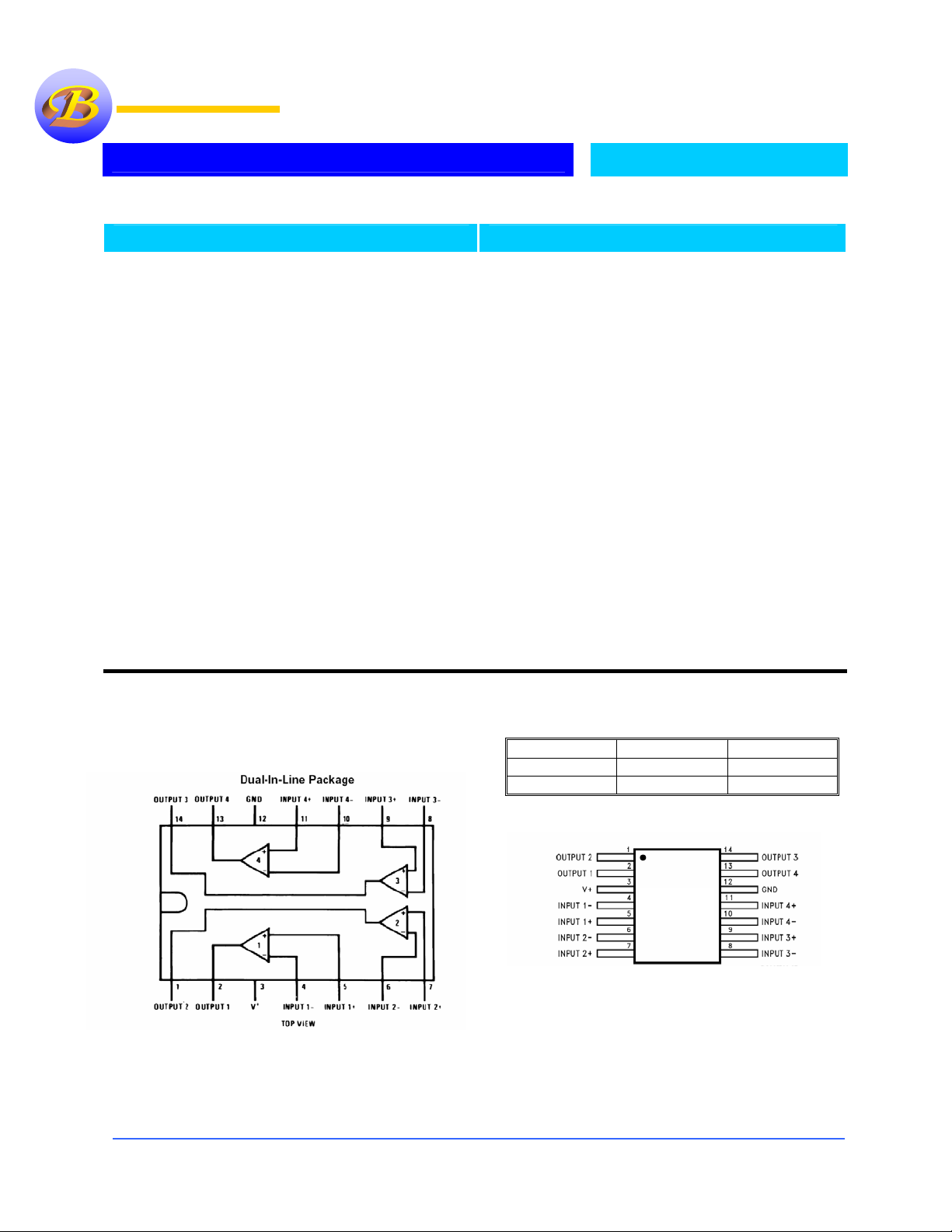
Pin Connection
LM339
Features
• Wide supply voltage range
• LM339 is 2 to 36 VDC or – 1 to – 18
• Very low supply current drain ( 0.8 mA) —
independent of supply voltage
• Low input biasing current: 25 nA
• Low input offset current: – 5 nA n Offset
voltage: – 3 mV
• Input common- mode voltage range
includes GND
• Differential input voltage range equal to the
power supply voltage
• Low output saturation voltage: 250 mV at 4
mA
• Output voltage compatible with TTL, DTL,
ECL, MOS and CMOS logic systems
Ordering Information
Devices Package Temp.
LM339M SO-14
LM339P 14-DIP
LM339
0 °C to 70 °C
0 °C to 70 °C
Bay Linear, Inc
2418 Armstrong Street, Livermore, CA 94550 Tel: (925) 606-5950, Fax: (925) 940-9556 www.baylinear.com
Page 2
LM339
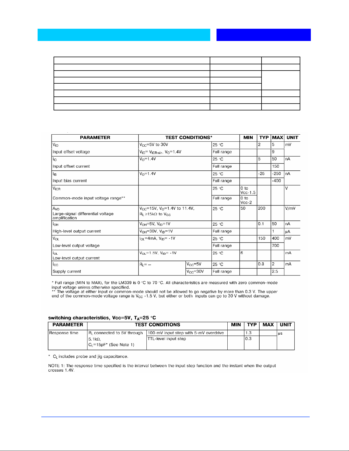
Absolute Maximum Rating
Parameter LM339 Unit
Supply Voltage 36 V
Differential Input Voltage 36
Input Voltage -0.3 to 36
Input Current 50
Storage Temperature 0 to 70
Lead Temperature (solder 10 Second) 260
ESD 250 V
V
V
mA
°C
°C
Electrical Characteristics
(VCC = 5V; TJ=25°C , unless otherwise specified)
Bay Linear, Inc
2418 Armstrong Street, Livermore, CA 94550 Tel: (925) 606-5950, Fax: (925) 940-9556 www.baylinear.com
Page 3

Advance Information- These data sheets contain descriptions of products that are in development. The specifications are based on the engineering calculations,
computer simulations and/ or initial prototype evaluation.
Preliminary Information- These data sheets contain minimum and maximum specifications that are based on the initial device characterizations. These limits are
subject to change upon the completion of the full characterization over the specified temperature and supply voltage ranges.
The application circuit examples are only to explain the representative applications of the devices and are not intended to guarantee any circuit
design or permit any industrial property right to other rights to execute. Bay Linear takes no responsibility for any problems related to any
industrial property right resulting from the use of the contents shown in the data book. Typical parameters can and do vary in different
applications. Customer’s technical experts must validate all operating parameters including “ Typical” for each customer application.
LIFE SUPPORT AND NUCLEAR POLICY
Bay Linear products are not authorized for and should not be used within life support systems which are intended for surgical
implants into the body to support or sustain life, in aircraft, space equipment, submarine, or nuclear facility applications without
the specific written consent of Bay Linear President.
Bay Linear, Inc
2418 Armstrong Street, Livermore, CA 94550 Tel: (925) 606-5950, Fax: (925) 940-9556 www.baylinear.com
 Loading...