

Page 1
现货库存、技术资料、百科信息、热点资讯,精彩尽在鼎好!
UNISONIC TECHNOLOGIES CO., LTD
LM339
LINEAR INTEGRATED CIRCUIT
QUAD DIFFERENTIAL
COMPARATOR
DESCRIPTION
The UTC LM339 consists of four independent voltage
comparators, designed specifically to operate from a single
power supply over a wide voltage range.
FEATURES
*Signal or dual supply operation.
*Wide operating supply range (Vcc=2V~36V).
*Input common-mode voltage includes ground.
*Low supply current drain I
*Open collector outputs for wired and connection.
*Low input bias current I
*Low output saturation voltage.
*Output compatible with TTL, DTL, and CMOS logic system.
=0.8mA (Typical).
F
=25nA (Typical).
BIAS
SOP-14
TSSOP-14
DIP-14
*Pb-free plating product number: LM339L
ORDERING INFORMATION
Order Number
Normal Lead free
LM339–S14-R LM339L –S14-R SOP-14 Tape & Reel
LM339–S14-T LM339L –S14-T SOP-14 Tube
LM339–P14-R LM339L –P14-R TSSOP-14 Tape & Reel
LM339–P14-T LM339L –P14-T TSSOP-14 Tube
LM339–D14-T LM339L –D14-T DIP-14 Tube
Package Packing
www.unisonic.com.tw 1
Copyright © 2005 Unisonic Technologies Co., LTD QW-R104-001.D
Page 2
LM339 LINEAR INTEGRATED CIRCUIT
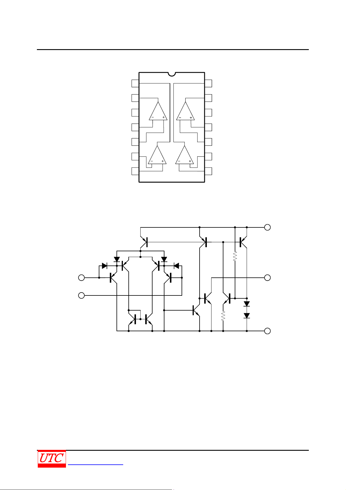
PIN CONFIGURATION
OUT 2
OUT 1
1
2
OUT 3
14
OUT 4
13
BLOCK DIAGRAM
Only one section
D1
IN (-)
IN (+)
3
Vcc
4
IN 1(-)
5
IN 1(+)
6
IN 2(-)
7
IN 2(+)
T9
D2 D3
T2
T1
T3
T4
T6T5
GND
12
IN 4(+)
11
IN 4 (-)
10
9
IN 3(+)
8
IN 3 (-)
Vcc
T11
T10
D4
R2
OUT
T8
T12
R1
D5
D6
T7
GND
UNISONIC TECHNOLOGIES CO., LTD 2
www.unisonic.com.tw QW-R104-001.D
Page 3

LM339 LINEAR INTEGRATED CIRCUIT
ABSOLUTE MAXIMUM RATINGS (Ta=25°C)
PARAMETER SYMBOL RATINGS UNIT
Supply Voltage Vcc +- 18 or 36 V
Differential input Voltage VI(
Input Voltage VIN -0.3~36 V
Power Dissipation PD 570 mW
Junction Temperature TJ 125 °C
Operating Temperature T
Storage Temperature T
Note 1. Absolute maximum ratings are those values beyond which the device could be permanently damaged.
Absolute maximum ratings are stress ratings only and functional device operation is not implied.
2. The device is guaranteed to meet performance specification within 0℃ ~ 70 ℃ operating temperature range
and assured by design from –20℃ ~ +85℃.
ELECTRICAL CHARACTERISTICS
(Vcc=5.0V, Ta=25°C, All voltage referenced to GND unless otherwise specified)
PARAMETER SYMBOL TEST CONDITIONS MIN TYP. MAX UNIT
Input Offset Voltage V
Input Offset Current I
Input Bias Current I
Input Common-Mode Voltage
Range
V
Supply Current Icc
V
I(OFF)
V
+-2.3 +-50 nA
I(OFF)
57 250 nA
BIAS
0 Vcc-1.5 V
IN(R)
R
Large Signal Voltage Gain GV Vcc=15V, RL>15kΩ 50 200 V/mV
Large Signal Response Time tres
V
V
Response Time tres VRL=5V, RL=5.1kΩ 1400 ns
Output Sink Current I
Output Saturation Voltage V
VIN (-)>1V, VIN (+)=0V, V
SINK
VIN (-)>1V, VIN (+)=0V, I
SAT
V
Output Leakage Current I
LEAK
V
V
Differential Input Voltage VIN(
) 36 V
DIFF
) 36 V
DIFF
0 ~ +70 °C
OPR
-40 ~ 150 °C
STG
=0 ~ Vcc-1.5
CM
(p)=1.4V, Rs=0
OUT
=∞
L
=TTL logic wing
IN
=1.4V, VRL=5V, RL=5.1kΩ
REF
(+)=1V,VIN (-)=0
IN
(p)= 5V
OUT
(p)=30V
OUT
(p)<1.5V 6 18 mA
OUT
=4mA 140 400 mV
SINK
+-1.5 +-5.0 mV
1.1 2.0 mA
350 ns
0.1
1.0
nA
µA
UNISONIC TECHNOLOGIES CO., LTD 3
www.unisonic.com.tw QW-R104-001.D
Page 4

LM339 LINEAR INTEGRATED CIRCUIT
TYPICAL CHARACTERISTICS
Fig.1 Supply Current
2.2
2.0
1.8
1.6
1.4
1.2
1.0
0.8
Supply Current (mA)
0.6
0.4
0.2
0 5 10 15 20 25 30 35 40
Ta=-40℃
Ta=-25℃
Ta=25℃
Ta=70℃
RL=∞
Supply Voltage (V)
Fig.3 Output Saturation Voltage
1
10
1
-1
10
Ta=85℃
Saturation Voltage(V)
-2
10
Ta=25℃
-3
10
-2
10
Ta=-40℃
-1
10
1
Output Sink Current (mA)
1
10 10
Fig.2 Input Current
110
100
90
80
70
60
50
Input Current (mA)
40
30
20
10
0 5 10 15 20 25 30 35 40
Ta=-40℃
Ta=-25℃
Ta=25℃
Ta=70℃
Vcm=0VDC
Rcm=1GΩ
Supply Current (V)
Fig.4 Reponse Time For Various Input
Overdrive Negative Transition
50mV
Ta=25℃
Input Overdrive
20mV 5.0mV
Time ( µs)
0
(mV)
Input Voltage
-100
6.0
4.0
(V)
2.0
Output Voltage
2
0
0 0.4 0.8 1.2 1.6
Fig.5 Reponse Time For Various Input
Overdrive Positive Transition
100
0
6.0
4.0
2.0
Output Voltage (V) Input Voltage (mV)
Input Overdrive
0
0 0.4 0.8 1.2 1.6
Ta=25℃
50mV 20mV 5.0mV
Time ( µs)
UNISONIC TECHNOLOGIES CO., LTD 4
www.unisonic.com.tw QW-R104-001.D
Page 5

LM339 LINEAR INTEGRATED CIRCUIT
TYPICAL CHARACTERISTICS(cont.)
Fig.6
3
2
1
Input Voltage (V)Output Voltage (V)
0
3
2
1
RL=2kΩ
Vcc=15V
Output Voltgae (V)
Fig.7 Voltage Follower Pulse Response
(Small Signal)
450
400
350
300
0
010
20 30 40
50
Time ( µs)
Fig.8 Large Signal Frequency Response
15
Vi
10
5
Output Swing (Vp-p)
0
35
4
1010
Frequency (Hz)
+15V
100k
1k
+7V
2k
6
10
10
Fig.10 Output Characteristics Current Sinking
10
275
0123456789
Time ( µs)
Fig.9 Output Characteristics
Current Sourcing
8
7
Ta=25℃
6
5
4
Vcc/2
Vcc
Vo
Io
3
Output Refference Vcc (V)
2
1
-3
10
-2
10
-1
10
10
Output Source Current (mA)
Fig.11 Current Limiting
60
2
101
1
40
Vcc=+5V
Output Voltage (V)
Vcc=+30V
Vcc=+15V
-1
10
Vcc/2
Vcc
Output Current (mA)
Vo
Io
20
-3
10
-2
10
-1
10
110210
Output Sink Current (mA)
0
-50 -25
25 50 75 100
0
Temperature (℃)
UNISONIC TECHNOLOGIES CO., LTD 5
www.unisonic.com.tw QW-R104-001.D
Page 6

LM339 LINEAR INTEGRATED CIRCUIT
UTC assumes no responsibility for equipment failures that result from using products at values that
exceed, even momentarily, rated values (such as maximum ratings, operating condition ranges, or
other parameters) listed in products specifications of any and all UTC products described or contained
herein. UTC products are not designed for use in life support appliances, devices or systems where
malfunction of these products can be reasonably expected to result in personal injury. Reproduction in
whole or in part is prohibited without the prior written consent of the copyright owner. The information
presented in this document does not form part of any quotation or contract, is believed to be accurate
and reliable and may be changed without notice.
UNISONIC TECHNOLOGIES CO., LTD 6
www.unisonic.com.tw QW-R104-001.D
 Loading...