

Datasheet LM336AH-2.5, LM336BZ-2.5, LM136AH-2.5, LM336H-2.5, LM336Z-2.5 Datasheet (Linear Technology)
...Page 1
FEATURES
■
Guaranteed
■
Maximum 0.6Ω Dynamic Impedance
■
Adjustable for Minimum Temperature Coefficient
■
Wide Operating Current Range
Temperature Stability
U
APPLICATIO S
■
Reference for 5V Systems
■
8-Bit A/D and D/A Reference
■
Digital Voltmeters
■
Current Loop Measurement and Control Systems
■
Power Supply Monitor
, LTC and LT are registered trademarks of Linear Technology Corporation.
LM136-2.5/LM336-2.5
2.5V Reference
U
DESCRIPTIO
The LM136-2.5 is a general purpose shunt regulator diode
designed to operate over a wide current range while
maintaining good stability with time and temperature. The
third terminal allows either the temperature coefficient to
be minimized or the reference voltage to be adjusted
without changing the temperature coefficient. Because it
operates as a shunt regulator it can be used equally well as
a positive or negative reference.
The LM136-2.5 is available with initial tolerances as low as
1% in either a TO-46 metal can for hermetic requirements
or a low cost TO-92 plastic package.
Linear’s advanced design, test and process techniques
have optimized the LM136-2.5 to achieve superior performance and reliability over previous designs. For more
demanding precision reference applications requiring very
low initial tolerance and temperature coefficients, consult
the LT1009 data sheet. A typical 2.5V reference with trim
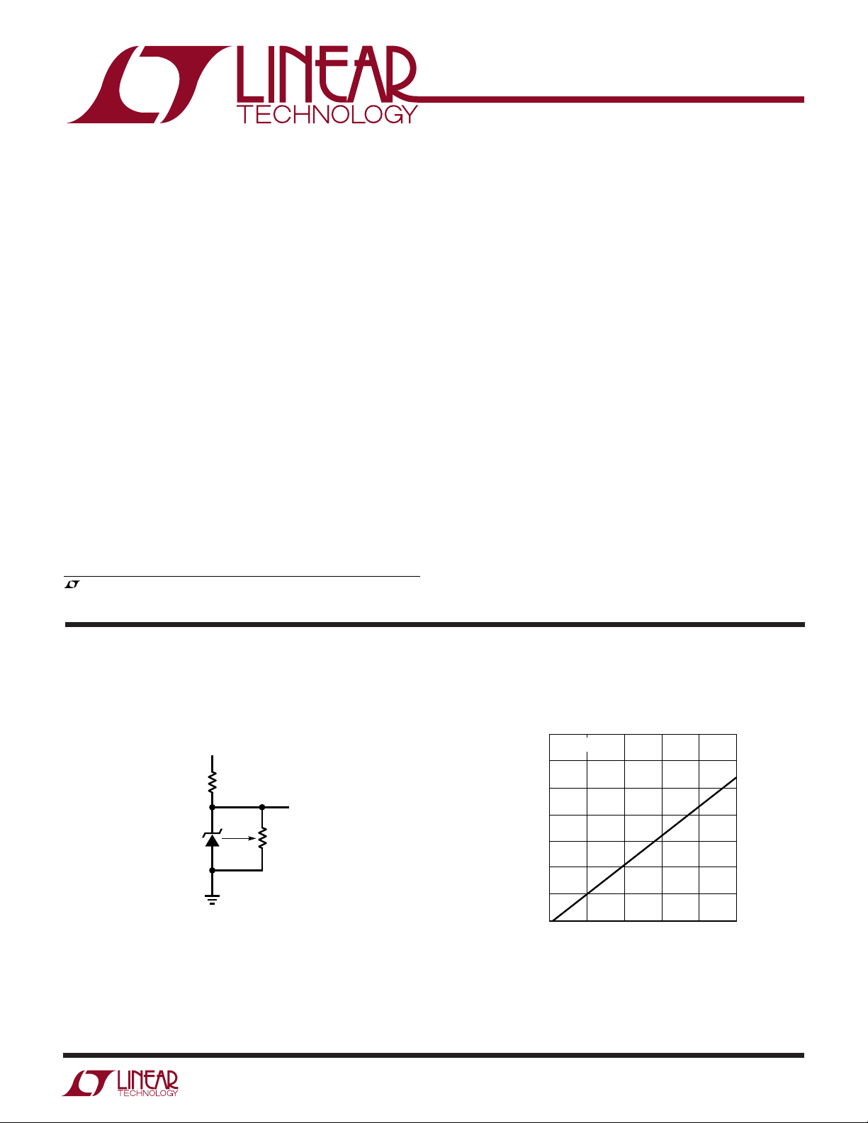
is shown below.
TYPICAL APPLICATIO
2.5V Reference
5V TO 35V
3.6k
LM336-2.5
*DOES NOT AFFECT
U
OUTPUT
10k*
TRIM
TEMPERATURE
COEFFICIENT
136/336 TA01a
Reverse Voltage Change
3.5
TA = 25°C
3.0
2.5
2.0
1.5
1.0
REVERSE VOLTAGE CHANGE (mV)
0.5
0
24 810
0
REVERSE CURRENT (mA)
6
136/336 TA01b
1
Page 2
LM136-2.5/LM336-2.5
WW
W
ABSOLUTE AXI U RATI GS
U
(Note 1)
Operating Temperature Range
LM136-2.5 (OBSOLETE) .............. –55°C to 125°C
LM336-2.5 .............................................. 0°C to 70°C
Storage Temperature Range ................. –65°C to 150°C
UUW
PACKAGE/ORDER I FOR ATIO
BOTTOM VIEW
+
ADJ
–
H PACKAGE
3-LEAD TO-46 METAL CAN
T
= 150°C, θJA = 440°C/W
JMAX
(NOTE 2)
OBSOLETE PACKAGE
Consider the Z Packages for Alternate Source
ORDER PART
NUMBER
LM136H-2.5
LM136AH-2.5
LM336H-2.5
LM336AH-2.5
Lead Temperature (Soldering, 10 sec).................. 300°C
Reverse Current.................................................... 15mA
Forward Current ................................................... 10mA
BOTTOM VIEW
+
ADJ
–
ORDER PART
NUMBER
LM336Z-2.5
LM336BZ-2.5
Z PACKAGE
3-LEAD PLASTIC TO-92
T
= 150°C, θJA = 160°C/W
JMAX
(NOTE 2)
Consult LTC Marketing for parts specified with wider operating temperature ranges.
ELECTRICAL CHARACTERISTICS
The ● denotes the specifications which apply over the full operating
temperature range, otherwise specifications are at TA = 25°C. (Note 2)
LM136/LM136A LM336/LM336B
SYMBOL PARAMETER CONDITIONS MIN TYP MAX MIN TYP MAX UNITS
V
∆V
∆I
r
∆V
∆Temp T
∆V
∆Time
Note 1: Absolute Maximum Ratings are those values beyond which the life
of a device may be impaired.
Note 2: The LT1009 is an improved, low cost, pin for pin replacement for
the “A” and “B” versions. For further information consult the LT1009 data
sheet.
Reverse Breakdown Voltage TA = 25°C, IR = 1mA
Z
Reverse Breakdown Change 400µA ≤ IR ≤ 10mA
Z
with Current TA = 25°C 2.6 6 2.6 10 mV
R
Reverse Dynamic Impedance IR = 1mA
Z
Temperature Stability VR Adjusted to 2.490V, IR = 1mA,
Z
Long Term Stability TA = 25°C ± 0.1°C, IR = 1mA 20 20 ppm/kHr
Z
LM136/LM336 2.440 2.490 2.540 2.390 2.490 2.590 V
LM136A/LM336B 2.465 2.490 2.515 2.440 2.490 2.540 V
T
≤ TA ≤ T
MIN
T
=25°C 0.2 0.6 0.2 1.0 Ω
A
≤ TA ≤ T
T
MIN
≤ TA ≤ T
MIN
MAX
MAX
(See Figure 1) ● 12 18 1.8 6 mV
MAX
● 3.0 10 3.0 12 mV
● 0.4 1.0 0.4 1.4 Ω
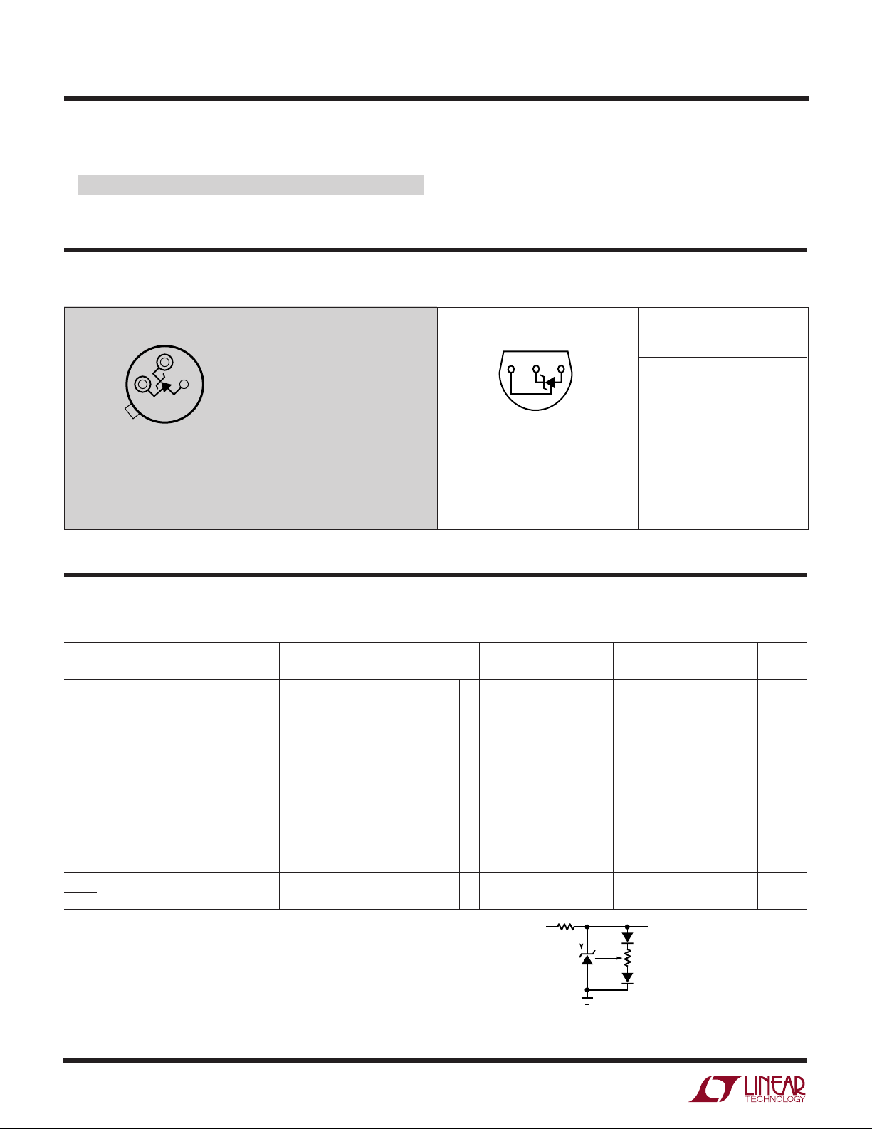
+
V
R
1mA
*
2.490V
†
D1
D1, D2 1N4148
* ADJUST TO 2.490
5k
†
ANY SILICON
SIGNAL DIODE
†
D2
136/336 F01
2
Figure 1. Adjusting the LM336 for
Minimum Temperature Coefficient
Page 3

UW
TYPICAL PERFOR A CE CHARACTERISTICS
LM136-2.5/LM336-2.5
Reverse Characteristics
–1
10
–2
10
–3
10
Tj = 25°C
–4
Tj = 125°C
REVERSE CURRENT (A)
10
Tj = –55°C
–5
10
0.6
1.0
1.4
REVERSE VOLTAGE (V)
1.8
Dynamic Impedance
100
IR = 1mA
≤ 125°C
–55°C ≤ T
j
10
1
DYNAMIC IMPEDANCE (Ω)
0.1
10 100 1k 10k 100k
FREQUENCY (Hz)
2.2
136/336 • G01
136/336 G04
2.6
Forward Characteristics
1.2
Tj = 25°C
1.0
0.8
0.6
0.4
FORWARD VOLTAGE (V)
0.2
0
0.001
0.01 0.1 1 10
FORWARD CURRENT (mA)
Zener Noise Voltage
250
200
150
NOISE (nV/√Hz)
100
50
10
100 1k
FREQUENCY (Hz)
IR = 1mA
T
10k
136/336 G02
= 25°C
j
136/336 G05
100k
Temperature Drift
2.59
IR = 1mA
2.57
2.55
2.53
2.51
2.49
2.47
2.45
REVERSE VOLTAGE (V)
2.43
2.41
2.39
2.37
–35
–55
TEMPERATURE (°C)
Response Time
3.5
3.0
2.5
2.0
1.5
1.0
0.5
0
VOLTAGE SWING (V)
12
8
4
0
INPUT
0
45 65
255–15
OUTPUT
5.1k
INPUT
120
TIME (µs)
85 105
136/336 G03
OUTPUT
136/336 G06
125
W
SCHE ATIC DIAGRA
Q2
Q1
Q3 Q5
Information furnished by Linear Technology Corporation is believed to be accurate and reliable.
However, no responsibility is assumed for its use. Linear Technology Corporation makes no representation that the interconnection of its circuits as described herein will not infringe on existing patent rights.
W
20pF
Q7
10k
Q4 Q6
Q8
30pF
Q12 Q14
50k
Q9
Q11Q10
Q13
2k 1.1k
Q15
24k
Q16
Q17
Q18
6.6k24k
500Ω
30k
6.6k
136/336 SD
+
ADJ
–
3
Page 4

LM136-2.5/LM336-2.5
–
+
1N4148
1N4148
10k
+
+
*LM336Z-2.5
*
OP-07CH
2
3
4
6
7
1µF
20µF
20µF
10k
10k
100k
1k
1k
2.5V
V
IN
≥ 6V
136/336 TA05
U
TYPICAL APPLICATIO S
Wide Supply
Range, Reference
3.6V TO 40V
+
V
LM334
–
V
LM336-2.5
R
62Ω
136/336 TA02
Low Temperature
Coefficient Power Regulator
LT317A
V
IN
IN
ADJ
*
ADJUST R2
FOR 3.75V
ACROSS R1
OUT
1.2k
1N4148
LM336
1N4148
PACKAGE DESCRIPTIO
H Package
2-Lead and 3-Lead TO-46 Metal Can
(Reference LTC DWG # 05-08-1340)
0.209 – 0.219
(5.309 – 5.537)
0.178 – 0.195
(4.521 – 4.953)
0.500
(12.700)
REFERENCE
PLANE
0.036 – 0.046
(0.914 – 1.168)
*
LEAD DIAMETER IS UNCONTROLLED BETWEEN THE REFERENCE PLANE
AND 0.045" BELOW THE REFERENCE PLANE
**
FOR SOLDER DIP LEAD FINISH, LEAD DIAMETER IS
MIN
0.016 – 0.021**
(0.406 – 0.533)
DIA
0.100
0.050
(2.540)
(1.270)
TYP
TYP
PIN 1
45°
0.085 – 0.105
(2.159 – 2.667)
*
0.025
(0.635)
MAX
0.050
(1.270)
TYP
FOR 3-LEAD PACKAGE ONLY
0.028 – 0.048
(0.711 – 1.219)
H02/03(TO-46) 1098
0.016 – 0.024
(0.406 – 0.610)
R2*
10k
R1
375Ω
2k
136/336 TA03
U
Switchable ±1.25V
Low Noise 2.5V Buffered Reference
Bipolar Reference
5V
V
OUT
5V
–5V
5k
5k
2N3904
*
2N3906
*LM336-2.5
–5V
5k
10k
1%
OUT
9.76k
1%
500Ω
136/336 TA04
Z Package
3-Lead Plastic TO-92 (Similar to TO-226)
(Reference LTC DWG # 05-08-1410)
10° NOM
0.180 ± 0.005
(4.572 ± 0.127)
(2.286)
0.050
UNCONTROLLED
LEAD DIMENSION
(1.270)
MAX
0.016 ± 0.003
(0.406 ± 0.076)
0.060 ± 0.010
(1.524 ± 0.254)
0.90
NOM
0.140 ± 0.010
(3.556 ± 0.127)
5°
NOM
0.015 ± 0.002
(0.381 ± 0.051)
0.098 +016/–0.04
(2.5 +0.4/–0.1)
2 PLCS
TO-92 TAPE AND REEL
REFER TO TAPE AND REEL SECTION OF
LTC DATA BOOK FOR ADDITIONAL INFORMATION
Z3 (TO-92) 0401
0.060 ± 0.005
(1.524± 0.127)
DIA
0.180 ± 0.005
(4.572 ± 0.127)
0.500
(12.70)
MIN
0.050
(1.27)
BSC
OBSOLETE PACKAGE
●
www.linear.com
RELATED PARTS
PART NUMBER DESCRIPTION COMMENTS
LT1009 Precision 2.5V Shunt Reference 0.2% Max Initial Tolerance
4
Linear Technology Corporation
1630 McCarthy Blvd., Milpitas, CA 95035-7417
(408) 432-1900 ● FAX: (408) 434-0507
136336fa LT/CP 0801 1.5K REV A • PRINTED IN USA
LINEAR TECHNOLOG Y CORPORATION 1986
 Loading...