

Page 1
August 1989
LM3361A Low Voltage/Power Narrow Band FM IF System
LM3361A Low Voltage/Power Narrow Band FM IF System
General Description
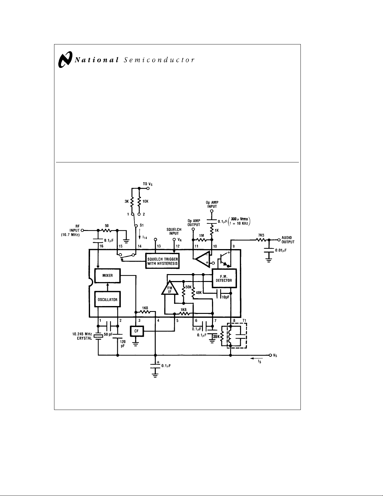
The LM3361A contains a complete narrow band FM demodulation system operable to less than 2V supply voltage.
Blocks within the device include an oscillator, mixer, FM IF
limiting amplifier, FM demodulator, op amp, scan control,
and mute switch. The LM3361A is similar to the MC3361
with the following improvements: the LM3361A has higher
voltage swing both at the op amp and audio outputs. It also
has lower nominal drain current and a squelch circuit that
draws significantly less current than the MC3361. Device
pinout functions are identical with some slightly different operating characteristics.
Block Diagram and Test Circuit
Features
Y
Functions at low supply voltage (less than 2V)
Y
Highly sensitive (b3 dB limiting at 2.0 mV input typical)
Y
High audio output (increased 6 dB over MC3361)
Y
Low drain current (2.8 mA typ., V
Y
Minimal drain current increase when squelched
Y
Low external parts count
CC
e
3.6V)
Order Number LM3661AM
or LM3361AN
T1-TOKO RMC-2A6597HM
CF-MURATA CFU 455E
TL/H/5586– 1
See NS Package Number
M16A or N16E
C
1995 National Semiconductor Corporation RRD-B30M115/Printed in U. S. A.
TL/H/5586
Page 2
Absolute Maximum Ratings
If Military/Aerospace specified devices are required,
please contact the National Semiconductor Sales
Office/Distributors for availability and specifications.
Package Dissipation (Note 1) 1500 mW
Power Supply Voltage (V
RF Input Voltage (V
Mute Function (pin 14)
Operating Ambient Temperature Range 0§Ctoa70§C
Storage Temperature Range
)12V
S
l
3.6V) 1 Vrms
S
b
0.7 to 5 Vp
b
55§Ctoa150§C
Soldering Information
Dual-In-Line Package
Soldering (10 seconds) 260
Small Outline Package
Vapor Phase (60 seconds) 215
Infrared (15 seconds) 220
See AN-450 ‘‘Surface Mounting Methods and Their Effect
on Product Reliability’’ for other methods of soldering surface mount devices.
C
§
C
§
C
§
Parameters Guaranteed By Electrical Testing
(Test ckt., T
e
A
Supply Voltage Range V
Supply Current
Squelch Off I
Squelch On I
RF Input forb3 dB Limiting RF Input 2.0 6.0 mV
Recovered Audio at Audio Output Audio Output 200 350 mV
Audio Out DC V
Op Amp Gain V11/V
Op Amp Output DC V
Op Amp Input Bias Current (V
Scan Voltage
Pin 12 high (2V) V
Pin 12 Low (0V) V
Mute Switch Impedance, Pin 12e0V DV14/DI
Switch S1 from pos.1 to pos.2
25§C, V
e
S
3.6V, f
e
10.7 MHz, D f
O
e
g
3 kHz, f
e
1 kHz, 50X source)
MOD
Parameter Measure Min Typ Max Units
S
S
S
9
IN
10
b
V11)/1MX 20 75 nA
10
13
13
14
2.0 3.6 9.0 V
2.8 5.0 mA
3.6 6.0 mA
1.2 1.5 1.8 V
40 55 dB
0.4 0.7 V
0 0.5 V
3.0 3.4 V
15 30 X
RMS
DC
DC
DC
DC
Design Parameters Not Tested or Guaranteed
Mixer Conversion Gain (Note 2) 46 V/V
Mixer Input Resistance 3.6 kX
Mixer Input Capacitance 2.2 pF
Detector Output Impedance 500 X
Squelch Hysterisis 100 mV
Mute Off Impedance (measure pin 14 with pin 12
@
Squelch Threshold 0.65 V
Detector Center Frequency Slope 0.15 V/kHz
Note 1. For operation above 25§C ambient temperature, the device must be derated based on 150§C maximum junction temperature and a thermal resistance i
of 80§C/W.
Note 2. Mixer gain is supply dependent and effects overall sensitivity accordingly (See Typical Performance Characteristics).
Typ
2V) 10 MX
DC
JA
Coils:
Toko America
1250 Feehanville Drive
Mount Prospect, IL 60056
(312) 297-0070
Filters:
Murata
2200 Lake Park Drive
Smyrna, GA 30080
(404) 436-1300
2
Page 3

Typical Performance Characteristics (Test Circuits)
TL/H/5586– 2
3
Page 4

Internal Schematic
TL/H/5586– 3
4
Page 5

Applications Information (See Internal Schematic)
OSCILLATOR
The Colpitts type oscillator is internally biased with a regulated current source which assures proper operation over a
wide supply range. The collector, base, and emitter terminals are at pins 4, 1, and 2 respectively. The crystal, which
is used in the parallel resonant mode, may be replaced with
an appropriate inductor if the application does not require
the stability of a crystal oscillator. In this case, the resonant
frequency will be determined by the inductor in parallel with
the series combination of C1 and C2.
so Cte(C1)(C2)/(C1aC2)
e
and f
.159/0L(Ct)
O
MIXER
The mixer is double balanced to reduce spurious responses.
The upper pairs are switched by the oscillator while the RF
input is applied to the lower pair (pin 16). R43 sets the mixer
input impedance at 3.6 kX. The mixer output impedance of
1.8 kX will properly match the input impedance of a ceramic
filter which is used as a bandpass filter coupling the mixer
output to the IF limiting amplifier.
IF LIMITER
The IF amplifier consists of six differential gain stages, with
the input impedance set by R2 at 1.8 kX to properly terminate the ceramic filter driving the IF. The IF alone (without
mixer) has a
mV. The system bandwidth is limited to about 5 MHz due to
high impedances in the IF which are necessary to meet low
power requirements. The IF output is connected to the external quad coil at pin 8 via an internal 10 pF capacitor.
FM DEMOD AUDIO OUT
A conventional quadrature detector is used to demodulate
the FM signal. The Q of the quad coil, which is determined
by the external resistor placed across it, has multiple effects
on the audio output. Increasing the Q increases output level
but because of nonlinearities in the tank phase characteris-
b
3 dB limiting sensitivity of approximately 50
TL/H/5586– 4
tic, also increases distortion (see Typical Performance
Characteristics). For proper operation, the voltage swing on
pin 8 should be adequate to drive the upper rank of the
multiplier into switching (about 100 mVrms). This voltage
level is dependent on the internal 10 pF capacitor and the
tank R
phasis, the audio output at pin 9 is buffered by an emitter
follower.
OP AMP
The op amp inverting input (pin 10) which is internally referenced to 0.7V, receives dc bias from the output at pin 11
through the external feedback network. Because of the low
D.C. bias, maximum swing on the op amp output with 10%
distortion is 500 mVrms. This can be increased when operating on supplies over 2.3V by adding a resistor from the op
amp input to ground which raises the quiescent D.C. at the
output allowing more swing (see figure below for selection
of added resistor). The op amp is normally utilized as either
a bandpass filter to extract a specific frequency from the
audio output, such as a ring or dial tone, or as a high pass
filter to detect noise due to no input at the mixer. The latter
condition will generate a signal at the op amp output, which
when applied to pin 12 can mute the external audio amp.
For max swing: V
SQUELCH TRIGGER CIRCUIT
The squelch trigger circuit is configured such that a low bias
on the input (pin 12) will force pin 13 high (200 mV below
supply), where it can support at leasta1mAload, and pin
14 to be a low impedance, typically 15X to ground. Connecting pin 14 to a high impedance ground reference point
in the audio path between pin 9 and the audio amp will mute
the audio output. Pulling pin 12 above mute threshold
(0.65V) will force pin 13 to an impedance of about 60 kX to
ground and pin 14 will be an open circuit. There is 100 mV
of hysterisis at pin 12 which effectively prevents jitter.
voltage divider network. After detection and de-em-
p
e
b
(V
OUT
so (V
S
therefore
Increasing OP Amp Swing
VBE)/2 (from internal circuit)
S
b
VBE)/2e0.7#1
R2
R3
b
V
S
e
1.4
#
R2
a
R3
J
V
BE
b
1
J
TL/H/5586– 5
5
Page 6

Physical Dimensions inches (millimeters)
Molded Small Outline Package (M)
Order Number LM3361AM
NS Package Number M16A
LM3361A Low Voltage/Power Narrow Band FM IF System
Molded Dual-In-Line Package (N)
Order Number LM3361AN
NS Package Number N16E
LIFE SUPPORT POLICY
NATIONAL’S PRODUCTS ARE NOT AUTHORIZED FOR USE AS CRITICAL COMPONENTS IN LIFE SUPPORT
DEVICES OR SYSTEMS WITHOUT THE EXPRESS WRITTEN APPROVAL OF THE PRESIDENT OF NATIONAL
SEMICONDUCTOR CORPORATION. As used herein:
1. Life support devices or systems are devices or 2. A critical component is any component of a life
systems which, (a) are intended for surgical implant support device or system whose failure to perform can
into the body, or (b) support or sustain life, and whose be reasonably expected to cause the failure of the life
failure to perform, when properly used in accordance support device or system, or to affect its safety or
with instructions for use provided in the labeling, can effectiveness.
be reasonably expected to result in a significant injury
to the user.
National Semiconductor National Semiconductor National Semiconductor National Semiconductor
Corporation Europe Hong Kong Ltd. Japan Ltd.
1111 West Bardin Road Fax: (
Arlington, TX 76017 Email: cnjwge@tevm2.nsc.com Ocean Centre, 5 Canton Rd. Fax: 81-043-299-2408
Tel: 1(800) 272-9959 Deutsch Tel: (
Fax: 1(800) 737-7018 English Tel: (
National does not assume any responsibility for use of any circuitry described, no circuit patent licenses are implied and National reserves the right at any time without notice to change said circuitry and specifications.
Fran3ais Tel: (
Italiano Tel: (
a
49) 0-180-530 85 86 13th Floor, Straight Block, Tel: 81-043-299-2309
a
49) 0-180-530 85 85 Tsimshatsui, Kowloon
a
49) 0-180-532 78 32 Hong Kong
a
49) 0-180-532 93 58 Tel: (852) 2737-1600
a
49) 0-180-534 16 80 Fax: (852) 2736-9960
 Loading...