

Page 1
November 2002
LM3354-3.7
Regulated 90mA Buck-Boost Switched Capacitor DC/DC
Converter
LM3354-3.7 Regulated 90mA Buck-Boost Switched Capacitor DC/DC Converter
General Description
The LM3354 is a CMOS switched capacitor DC/DC converter that produces a regulated output voltage by automatically stepping up (boost) or stepping down (buck) the input
voltage. It accepts an input voltage between 2.5V and 5.5V.
The LM3354 is also available with standard output voltages
of 1.8V, 3.3V, 3.7V, 4.1V (ideal for white LED applications),
and 5.0V. If other output voltage options between 1.8V and
5.0V are desired, please contact your National Semiconductor representative.
The LM3354’s proprietary buck-boost architecture enables
up to 90mA of load current at an average efficiency greater
than 75%. Typical operating current is only 375 µA and the
typical shutdown current is only 2.3 µA.
The LM3354 is available in a 10-pin MSOP package. This
package has a maximum height of only 1.1 mm.
The high efficiency of the LM3354, low operating and shutdown currents, small package size, and the small size of the
overall solution make this device ideal for battery powered,
portable, and hand-held applications.
See the LM3352 for up to 200mA of output current or the
LM3355 for up to 50mA of output current.
Features
n Regulated V
n Standard output voltages of 1.8V, 3.3V, 4.1V, and 5.0V
also available
n Custom output voltages available from 1.8V to 5.0V in
100 mV increments with volume order
n 2.5V to 5.5V input voltage range
n Up to 90mA output current
>
n
75% average efficiency
n Uses few, low-cost external components
n Very small solution size
n 375 µA typical operating current
n 2.3 µA typical shutdown current
n 1 MHz typical switching frequency
n Architecture and control methods provide high load
current and good efficiency
n MSOP-10 package
n Over-temperature protection
with±3% accuracy
OUT
Applications
n White LED display backlights
n 1-cell Lilon battery-operated equipment including PDAs,
hand-held PCs, cellular phones
n Flat panel displays
n Hand-held instruments
n Li-Ion, NiCd, NiMH, or alkaline battery powered systems
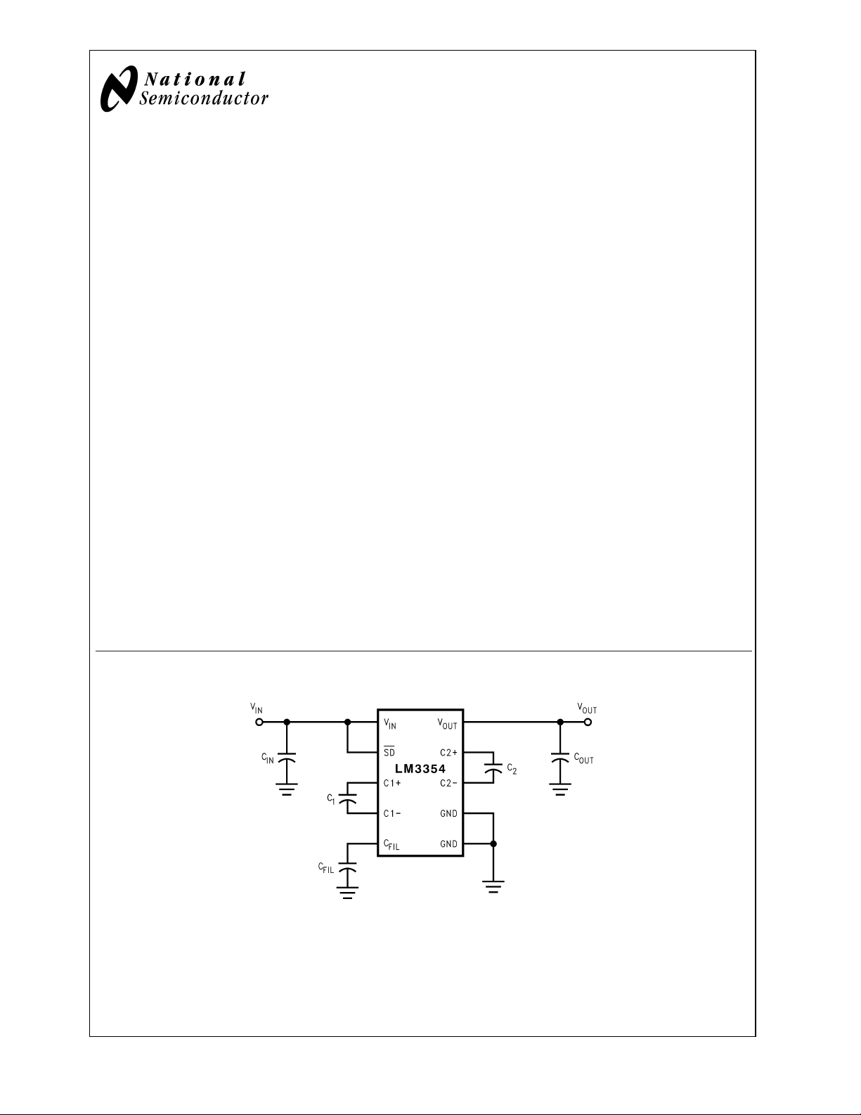
Typical Operating Circuit
20057301
© 2002 National Semiconductor Corporation DS200573 www.national.com
Page 2
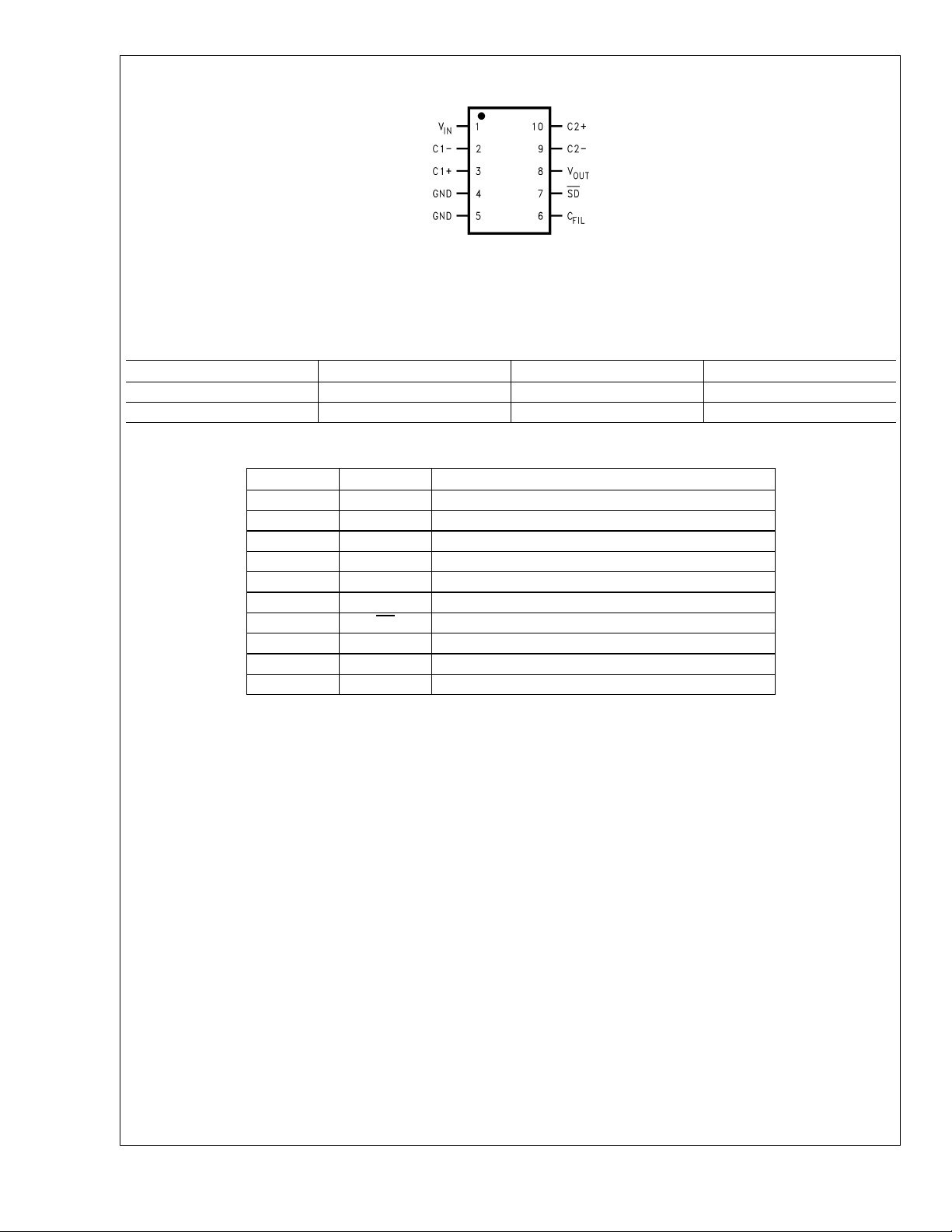
Connection Diagram
LM3354-3.7
Top View
MSOP-10 Pin Package
See NS Package Number MM
20057302
Ordering Information
Order Number Package Type NSC Package Drawing Supplied As
LM3354MMX-3.7 MSOP-10 MUB10A 3.5k Units, Tape and Reel
LM3354MM-3.7 MSOP-10 MUB10A 1k Units, Tape and Reel
Pin Description
Pin Number Name Function
1V
2 C1− Negative Terminal for C1
3 C1+ Positive Terminal for C1
4 GND Ground
5 GND Ground
6C
7SD
8V
9 C2− Negative Terminal for C2
10 C2+ Positive Terminal for C2
IN
FIL
OUT
Input Supply Voltage
Filter Capacitor, a 1µF capacitor is recommended.
Shutdown, active low
Regulated Output Voltage
www.national.com 2
Page 3
LM3354-3.7
Absolute Maximum Ratings (Note 1)
If Military/Aerospace specified devices are required,
please contact the National Semiconductor Sales Office/
ESD Rating (Note 3)
Human Body Model
Machine Model
1.5 kV
Distributors for availability and specifications.
All Pins −0.5V to 5.6V
Power Dissipation (T
= 25˚C)
A
(Note 2) Internally Limited
(Note 2) 150˚C
T
JMAX
θ
(Note 2) 250˚C/W
JA
Storage Temperature −65˚C to +150˚C
Operating Ratings
Input Voltage (VIN) 2.5V to 5.5V
Output Voltage (V
Ambient Temperature (T
Junction Temperature (T
) 1.8V to 5.0V
OUT
) (Note 2) −40˚C to +85˚C
A
) (Note 2) −40˚C to +120˚C
J
Lead Temperature (Soldering, 5
sec.) 260˚C
Electrical Characteristics
Limits in standard typeface are for TA= 25˚C, and limits in boldface type apply over the full operating temperature range. Unless otherwise specified: C
= 0.33 µF; CIN= 10 µF; C
1=C2
Parameter Conditions Min
(Note 5)
LM3354-3.7
Output Voltage (V
OUT
)
Efficiency I
Output Voltage
Ripple
(Peak-to-Peak)
V
= (2.7, 5.5) V
IN
= (1, 70) mA
I
L
V
= (2.8, 4.0) V
IN
= (1, 90) mA
I
L
V
= (4.3, 5.5) V
IN
= (1, 90) mA
I
L
=15mA 75
LOAD
I
=70mA 70
LOAD
=50mA
I
LOAD
=10µF
C
OUT
3.589/3.552 3.7 3.811/3.848
3.589/3.552 3.7 3.811/3.848
3.589/3.552 3.7 3.811/3.848
ceramic
LM3354-ALL OUTPUT VOLTAGE VERSIONS
Operating Quiescent
Current
Shutdown Quiescent
Current
Switching
Measured at Pin
;
V
IN
= 0A (Note 6)
I
LOAD
SD Pin at 0V (Note
7)
0.6 1 1.4 MHz
Frequency
<
SD Input Threshold
2.5V
<
V
5.5V 0.2 V
IN
Low
SD Input Threshold
2.5V<V
<
5.5V 0.8 V
IN
IN
High
SD Input Current Measured at SD
Pin;
SD Pin = V
Note 1: “Absolute Maximum Ratings” indicate limits beyond which damage to the device may occur. Operating Ratings are conditions for which the device is
intended to be functional, but device parameter specifications may not be guaranteed. For guaranteed specifications and test conditions, see “Electrical
Characteristics”.
Note 2: As long as T
The 5V option requires that T
Note 3: The human body model is a 100 pF capacitor discharged through a 1.5 kΩ resistor into each pin. The machine model is a 200 pF capacitor discharged
directly into each pin.
Note 4: Typical numbers are at 25˚C and represent the most likely norm.
Note 5: All limits guaranteed at room temperature (standard typeface) and at temperature extremes (bold typeface). All room temperature limits are 100% tested
or guaranteed through statistical analysis. All limits at temperature extremes are guaranteed by correlation using standard Statistical Quality Control methods (SQC).
All limits are used to calculate Average Outgoing Quality Level (AOQL).
≤ +85˚C, all electrical characteristics hold true and the junction temperature should remain below +120˚C except for the 5V output option.
A
≤ +60˚C.
A
IN
= 5.5V
OUT
= 10 µF; C
(Note 4)
= 1 µF; VIN= 3.5V.
FIL
Typ
Max
(Note 5)
75 mV
375 475 µA
2.3 5 µA
IN
0.3 µA
Units
V
%
P-P
V
V
100V
www.national.com3
Page 4

Electrical Characteristics (Continued)
Note 6: The V
Note 7: The output capacitor C
LM3354-3.7
pin is forced to 200 mV above the typical V
OUT
is fully discharged before measurement.
OUT
. This is to insure that the internal switches are off.
OUT
www.national.com 4
Page 5

LM3354-3.7
Typical Performance Characteristics Unless otherwise specified T
vs. V
V
OUT
IN
Efficiency vs. V
20057341 20057342
IN
V
Load Transient Response
A
OUT
= 25˚C.
vs. V
IN
Operating Quiescent
Current vs. V
IN
20057320
20057324
Switching Frequency vs. V
20057314
IN
20057323
www.national.com5
Page 6

Typical Performance Characteristics Unless otherwise specified T
= 25˚C. (Continued)
A
LM3354-3.7
Maximum V
Ripple vs. C
OUT
OUT
20057332
Maximum V
Ripple vs. C
OUT
OUT
20057330
www.national.com 6
Page 7

Applications Information
LM3354-3.7
20057303
FIGURE 1. Block Diagram
Operating Principle
The LM3354 is designed to provide a step-up/step-down
voltage regulation in battery powered systems. It combines
switched capacitor circuitry, reference, comparator, and
shutdown logic in a single 10-pin MSOP package. The
LM3354 can provide a regulated voltage between 1.8V and
5.0V from an input voltage between 2.5V and 5.5V. It can
supply a load current up to 90 mA (refer to Electrical Char-
acteristics).
As shown in Figure 1, the LM3354 employs two feedback
loops to provide regulation in the most efficient manner
possible. The first loop is from V
COMP, the AND gate G
switch array. The comparator’s output is high when V
less than the reference V
gating the clock to the switch array. In this manner, charge is
transferred to the output only when needed. The second
loop controls the gain configuration of the switch array. This
loop consists of the comparator, the digital control block, the
phase generator, and the switch array. The digital control
block computes the most efficient gain from a set of five
gains based on inputs from the A/D and the comparator. The
gain signal is sent to the phase generator which then sends
the appropriate timing and configuration signals to the switch
array. This dual loop provides regulation over a wide range of
loads efficiently.
Since efficiency is automatically optimized, the curves for
vs. VINand Efficiency vs. VINin the Typical Perfor-
V
OUT
mance Characteristics section exhibit small variations. The
reason is that as input voltage or output load changes, the
digital control loops are making decisions on how to optimize
efficiency. As the switch array is reconfigured, small variations in output voltage and efficiency result. In all cases
where these small variations are observed, the part is operating correctly; minimizing output voltage changes and optimizing efficiency.
, the phase generator, and the
1
REF
through the comparator
OUT
. Regulation is provided by
OUT
Charge Pump Capacitor Selection
A 0.33 µF ceramic capacitor is suggested for C1 and C2. To
ensure proper operation over temperature variations, an
X7R dielectric material is recommended.
Filter Capacitor Selection
a) CAPACITOR TECHNOLOGIES
The three major technologies of capacitors that can be used
as filter capacitors for LM3354 are: i) tantalum, ii) ceramic
and iii) polymer electrolytic technologies.
is
i) Tantalum
Tantalum capacitors are widely used in switching regulators.
Tantalum capacitors have the highest CV rating of any technology; as a result, high values of capacitance can be obtained in relatively small package sizes. It is also possible to
obtain high value tantalum capacitors in very low profile
<
1.2 mm) packages. This makes the tantalums attractive
(
for low-profile, small size applications. Tantalums also possess very good temperature stability; i.e., the change in the
capacitance value, and impedance over temperature is relatively small. However, the tantalum capacitors have relatively
high ESR values which can lead to higher voltage ripple and
their frequency stability (variation over frequency) is not very
good, especially at high frequencies (
ii) Ceramic
Ceramic capacitors have the lowest ESR of the three technologies and their frequency stability is exceptionally good.
These characteristics make the ceramics an attractive
choice for low ripple, high frequency applications. However,
the temperature stability of the ceramics is bad, except for
the X7R and X5R dielectric types. High capacitance values
>
1 µF) are achievable from companies such as
(
Taiyo-yuden which are suitable for use with regulators. Ceramics are taller and larger than the tantalums of the same
capacitance value.
>
1 MHz).
www.national.com7
Page 8

Filter Capacitor Selection (Continued)
iii) Polymer Electrolytic
Polymer electrolytic is a third suitable technology. Polymer
LM3354-3.7
capacitors provide some of the best features of both the
ceramic and the tantalum technologies. They provide very
low ESR values while still achieving high capacitance val-
the same size. Polymers offer good frequency stability (comparable to ceramics) and good temperature stability (comparable to tantalums). The Aluminum Polymer Electrolytics
offered by Cornell-Dubilier and Panasonic, and the POSCAPs offered by Sanyo fall under this category.
Table 1 compares the features of the three capacitor tech-
nologies.
ues. However, their ESR is still higher than the ceramics,
and their capacitance value is lower than the tantalums of
TABLE 1. Comparison of Capacitor Technologies
Ceramic Tantalum
ESR Lowest High Low
Relative Height Low for Small Values (
<
10 µF); Taller for
Lowest Low
Higher Values
Relative Footprint Large Small Largest
Temperature Stability X7R/X5R-Acceptable Good Good
Frequency Stability Good Acceptable Good
<
V
Ripple Magnitude
OUT
V
Ripple Magnitude
OUT
dv/dt of V
OUT
Ripple@All Loads Lowest High Low
@
50 mA Low High Low
>
@
100 mA Low Slightly Higher Low
Polymer
Electrolytic
b) CAPACITOR SELECTION
low input and output ripple as well as size a 10 µF polymer
electrolytic or ceramic, or 15 µF tantalum capacitor is rec-
i) Output Capacitor (C
The output capacitor C
the output ripple voltage so C
lected. The graphs titled V
Performance Characteristics section show how the ripple
voltage magnitude is affected by the C
capacitor technology. These graphs are taken at the gain at
which worst case ripple is observed. In general, the higher
the value of C
, the lower the output ripple magnitude. At
OUT
lighter loads, the low ESR ceramics offer a much lower V
ripple than the higher ESR tantalums of the same value. At
higher loads, the ceramics offer a slightly lower V
magnitude than the tantalums of the same value. However,
the dv/dt of the V
OUT
electrolytics is much lower than the tantalums under all load
conditions. The tantalums are suggested for very low profile,
small size applications. The ceramics and polymer electrolytics are a good choice for low ripple, low noise applications
where size is less of a concern.
ii) Input Capacitor (C
The input capacitor C
input ripple voltage, and to a lesser degree the V
A higher value C
IN
)
OUT
directly affects the magnitude of
OUT
OUT
should be carefully se-
OUT
Ripple vs. C
OUT
value and the
OUT
in the Typical
OUT
ripple
OUT
ripple with the ceramics and polymer
)
IN
directly affects the magnitude of the
IN
OUT
ripple.
will give a lower VINripple. To optimize
ommended. This will ensure low input ripple at 90 mA load
current. If lower currents will be used or higher input ripple
can be tolerated then a smaller capacitor may be used to
reduce the overall size of the circuit. The lower ESR ceram-
ics and polymer electrolytics achieve a lower V
ripple than
IN
the higher ESR tantalums of the same value. Tantalums
make a good choice for small size, very low profile applica-
tions. The ceramics and polymer electrolytics are a good
choice for low ripple, low noise applications where size is
less of a concern. The 10 µF polymer electrolytics are physi-
cally much larger than the 15 µF tantalums and 10 µF
ceramics.
iii) C
FIL
A 1 µF, X7R ceramic capacitor should be connected to pin
. This capacitor provides the filtering needed for the
C
FIL
internal supply rail of the LM3354.
Of the different capacitor technologies, a sample of vendors
that have been verified as suitable for use with the LM3354
are shown in Table 2.
TABLE 2. Capacitor Vendor Information
Manufacturer Tel Fax Website
Ceramic Taiyo-yuden (408) 573-4150 (408) 573-4159 www.t-yuden.com
AVX (803) 448-9411 (803) 448-1943 www.avxcorp.com
Sprague/Vishay (207) 324-4140 (207) 324-7223 www.vishay.com
Tantalum
Nichicon (847) 843-7500 (847) 843-2798 www.nichicon.com
Polymer Electrolytic Cornell-Dubilier (ESRD) (508) 996-8561 (508) 996-3830 www.cornell-dubilier.com
Sanyo (POSCAP) (619) 661-6322 (619) 661-1055 www.sanyovideo.com
www.national.com 8
Page 9

LM3354-3.7
Maximum Load Under Start-Up
Due to the LM3354’s unique start-up sequence, it is not able
to start up under all load conditions. Starting with 60 mA or
less will allow the part to start correctly under any temperature or input voltage conditions. After the output is in regulation, any load up to the maximum as specified in the
Electrical Characteristics may be applied. Using a Power On
Reset circuit, such as the LP3470, is recommended if
greater start up loads are expected. Under certain conditions
the LM3354 can start up with greater load currents without
the use of a Power On Reset Circuit.
Typical Application Circuits
Thermal Protection
During output short circuit conditions, the LM3354 will draw
high currents causing a rise in the junction temperature.
On-chip thermal protection circuitry disables the charge
pump action once the junction temperature exceeds the
thermal trip point, and re-enables the charge pump when the
junction temperature falls back to a safe operating point.
20057333
FIGURE 2. Basic Buck/Boost Regulator
FIGURE 3. Low Output Noise and Ripple Buck/Boost Regulator
20057315
www.national.com9
Page 10

Typical Application Circuits (Continued)
LM3354-3.7
20057340
FIGURE 4. White LED Driver
Driving Light Emitting Diodes
The LM3354 can be used to drive LED’s of nearly any color.
The 4.1V option is ideal for driving the White LED’s required
for the backlight of small color displays. Figure 4 shows the
circuit used to power White LED’s. The LED current is set by
the resistors R
by using the equation I
B
where VFis the typical forward voltage drop of the LED used.
The brightness of the diodes may be controlled using the
shutdown pin. A PWM signal on the shutdown pin may be
used to adjust the brightness by varying the duty cycle. A
signal between 60Hz and 200Hz may be used for best
linearity. In this case the equivalent LED current is approxi-
= (4.1V − VF)/R
LED
mately equal to the maximum current multiplied by the duty
cycle. Using frequencies above 200Hz may cause less linear
results as the charge and discharge time of the output
capacitor becomes more significant.
B
Layout Considerations
Due to the 1 MHz typical switching frequency of the LM3354,
careful board layout is a must. It is important to place the
capacitors as close to the IC as possible and to keep the
traces between the capacitors and the IC short and direct.
Use of a ground plane is recommended. Figure 5 shows a
typical layout as used in the LM3354 evaluation board.
FIGURE 5. Typical Layout, Top View (magnification 1.5X)
www.national.com 10
20057316
Page 11

Physical Dimensions inches (millimeters)
unless otherwise noted
LM3354-3.7 Regulated 90mA Buck-Boost Switched Capacitor DC/DC Converter
MSOP-10 Pin Package (MM)
For Ordering, Refer to Ordering Information Table
NS Package Number MUB10A
LIFE SUPPORT POLICY
NATIONAL’S PRODUCTS ARE NOT AUTHORIZED FOR USE AS CRITICAL COMPONENTS IN LIFE SUPPORT
DEVICES OR SYSTEMS WITHOUT THE EXPRESS WRITTEN APPROVAL OF THE PRESIDENT AND GENERAL
COUNSEL OF NATIONAL SEMICONDUCTOR CORPORATION. As used herein:
1. Life support devices or systems are devices or
systems which, (a) are intended for surgical implant
into the body, or (b) support or sustain life, and
whose failure to perform when properly used in
accordance with instructions for use provided in the
2. A critical component is any component of a life
support device or system whose failure to perform
can be reasonably expected to cause the failure of
the life support device or system, or to affect its
safety or effectiveness.
labeling, can be reasonably expected to result in a
significant injury to the user.
National Semiconductor
Corporation
Americas
Email: support@nsc.com
www.national.com
National Semiconductor
Europe
Fax: +49 (0) 180-530 85 86
Email: europe.support@nsc.com
Deutsch Tel: +49 (0) 69 9508 6208
English Tel: +44 (0) 870 24 0 2171
Français Tel: +33 (0) 1 41 91 8790
National Semiconductor
Asia Pacific Customer
Response Group
Tel: 65-2544466
Fax: 65-2504466
Email: ap.support@nsc.com
National Semiconductor
Japan Ltd.
Tel: 81-3-5639-7560
Fax: 81-3-5639-7507
National does not assume any responsibility for use of any circuitry described, no circuit patent licenses are implied and National reserves the right at any time without notice to change said circuitry and specifications.
 Loading...