

Page 1
LM3351
Switched Capacitor Voltage Converter
General Description
The LM3351 is a CMOS charge-pump voltage converter
which efficiently provides a 3.3V to 5V step-up, or 5V to 3.3V
step-down. The LM3351 is pin for pin compatible with the
LM3350 but consumes 66%less quiescent current. The
LM3351 uses four small, low cost capacitors to provide the
voltage conversion. It eliminates the cost, size and radiated
EMI related to inductor based circuits, or the power loss of a
linear regulator. Operating power conversion efficiency
greater than 90%provides ideal performance for battery
powered portable systems.
The architecture provides a fixed voltage conversion ratio of
3/2 or 2/3. Thus it can be used for other DC-DC conversions
as well.
Key Specifications
n 200 kHz switch frequency allows use of very small,
inexpensive capacitors.
Ordering Information
n 4.2Ω typical step-up output impedance
n 1.8Ω typical step-down output impedance
n 95%typical power conversion efficiency at 50 mA
n 250 nA typical shutdown current
n Low quiescent current extends battary life
Features
n Conversion of 3.3V to 5V, or 5V to 3.3V
n Small Mini SO-8 package
n No inductor required
Applications
n Any mixed 5V and 3.3V system
n Laptop computers and PDAs
n Handheld instrumentation
n PCMCIA cards
LM3351 Switched Capacitor Voltage Converter
December 1999
Order Number Package Type
LM3351MMX Mini SO-8 MUA08A S05A 3500 Units on Tape and Reel
LM3351MM Mini SO-8 MUA08A S05A 1000 Units on Tape and Reel
NSC Package
Drawing
Package
Marking
Supplied As
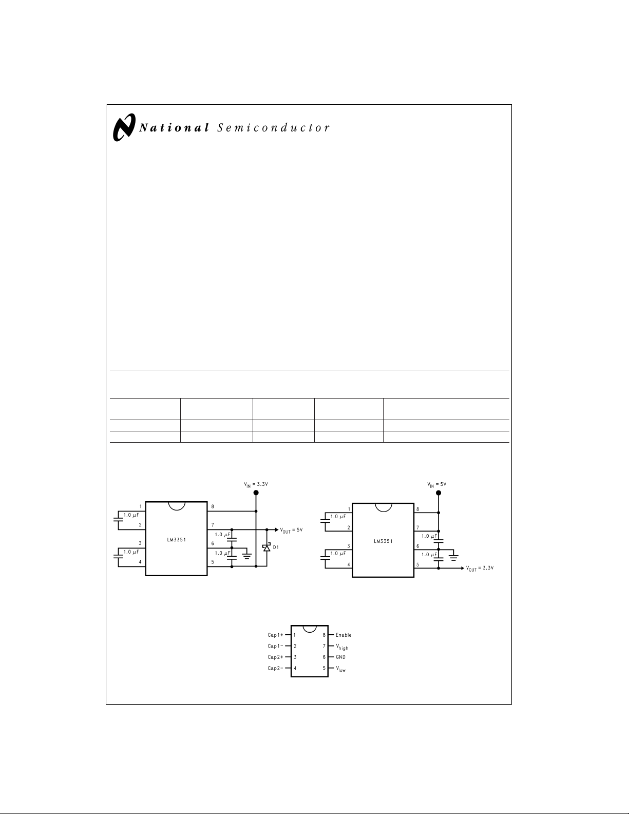
Basic Operating Circuits
Step-Up Converter
DS100146-1
Step-Down Converter
Connection Diagram
Mini SO8 Package
DS100146-3
Top View
DS100146-2
© 1999 National Semiconductor Corporation DS100146 www.national.com
Page 2
Absolute Maximum Ratings (Note 1)
If Military/Aerospace specified devices are required,
LM3351
please contact the National SemiconductorSalesOffice/
Distributors for availability and specifications.
Maximum Input Voltage, Step-Down 5.5V
Maximum Input Voltage, Step-Up 3.65V
Power Dissipation (P
(Note 2))
(Note 2) 250˚C/W
θ
ja
)(TA=25˚C,
D
500 mW
Storage Temperature −65˚C to +150˚C
Lead Temperature (Soldering, 10
secs)
ESD Susceptibility (Note 3) 2kV
Not short circuit protected.
Operating Conditions (Note 1)
Ambient Temperature Range −40˚C to + 85˚C
Tj Max (Note 2) 150˚C
Electrical Characteristics
3/2 Step-Up Voltage Converter
Specifications in standard type face are for Tj= 25˚C, and those with boldface type apply over full operating temperature
range. Unless otherwise specified, V
= 3.3V, V
in
Enable
= 3.3V, I
= 50 mA, C1,C2,Cinand C
load
Symbol Parameter Conditions Typ (Note 4) Limits (Note 5) Units
V
V
V
I
Q1
I
Q2
Z
f
SW
V
I
Enable
P
out
out
in
out
Enable
η
Output Voltage at
NL
No Load
Output Voltage at
FL
50 mA
Input Supply
Voltage Range
Quiescent Current Shutdown Mode, V
Quiescent Current Normal Mode, I
Output Source
Impedance
Switching
Frequency
Enable Threshold
Voltage
Leakage Current Current into ENABLE pin; ENABLE =
Power Efficiency 95
I
= 0 A 5.0 V
load
I
=50mA 4.7 V
load
3.3 V
= 0V,
=0 A; Current into pin V
I
load
pin V
Iow
I
=50mA 4.2 Ω
load
Enable
= 0A; Current into
Ioad
low
0.025 µA
1.1 mA
(Note 6) 200 kHz
1.7 V
0.025 µA
5V and all other pins at ground
=
1 µF.
out
2.5 V(Min)
3.65 V(Max)
3 µA(Max)
1.5 mA(Max)
6.25 Ω (Max)
125 kHz(Min)
275 kHz(Max)
1.0 V(Min)
2.5 V(Max)
1 µA(Max)
260˚C
%
Electrical Characteristics
2/3 Step-Down Voltage Converter
Specifications in standard type face are for Tj= 25˚C, and those with boldface type apply over full operating temperature
range. Unless otherwise specified, V
high
= 5V, V
Enable
= 5V, I
= 50 mA, C1,C2,Cinand C
load
Symbol Parameter Conditions Typ (Note 4) Limits (Note 5) Units
V
out
V
out
V
in
I
Q1
www.national.com 2
Output Voltage at
NL
No Load
Output Voltage at
FL
50 mA
Input Supply
Voltage Range
Quiescent Current Shutdown Mode, V
I
= 0 A 3.3 V
load
I
=50 mA 3.2 V
load
5V
=0 A; Current into pin V
I
load
Enable
= 0V,
high
0.25 µA
=
1 µF.
out
2.2 V(Min)
5.5 V(Max)
3 µA(Max)
Page 3
Electrical Characteristics
2/3 Step-Down Voltage Converter
Specifications in standard type face are for Tj= 25˚C, and those with boldface type apply over full operating temperature
range. Unless otherwise specified, V
Symbol Parameter Conditions Typ (Note 4) Limits (Note 5) Units
I
Q2
Z
out
f
SW
V
Enable
I
Enable
P
η
Note 1: Absolute maximum ratings indicate limits beyond which damage to the device may occur. Operating ratings indicate conditions for which the device is intended to befunctional, but do not guarantee specific performance limits. For guaranteed specifications and test conditions, see Electrical Characteristics. The guaranteed specifications apply only for the test conditions listed. Some performance characteristics may degrade when the device is not operated under the listed test
conditions.
Note 2: For operation at elevated temperatures, LM3351 must be derated based on package thermal resistance of θ
Note 3: The human body model is a 100 pF capacitor discharged through a 1.5 kW resistor into each pin.
Note 4: Typical numbers are at 25˚C and represent the most likely parametric norm.
Note 5: Limits are 100%production tested at 25˚C. Limits over the operating temperature range are guaranteed through correlation using Statistical Quality Control
(SQC) methods. The limits are used to calculate National’s Averaging Outgoing Quality Level (AOQL).
Note 6: The internal oscillator runs at 1.6 MHz, the output switches operate at one eighth of the oscillator frequency, f
Quiescent Current Normal Mode, I
Output Source
Impedance
Switching
Frequency
Enable Threshold
Voltage
Leakage Current Current into ENABLE pin; ENABLE =
Power Efficiency 95
= 5V, V
high
pin V
high
I
=50mA 1.8 Ω
load
(Note 6) 200 kHz
5V and all other pins at ground
(Continued)
= 5V, I
Enable
= 0A; Current into
Ioad
= 50 mA, C1,C2,Cinand C
load
0.8 mA
1.7 V
0.025 µA
=
1 µF.
out
1.0 mA(Max)
3 Ω(Max)
125 kHz(Min)
275 kHz(Max)
1.0 V(Min)
2.5 V(Max)
1 µA(Max)
and Tjmax, Tj=TA+θjaPD.
ja
=
.
8f
OSC
SW
%
LM3351
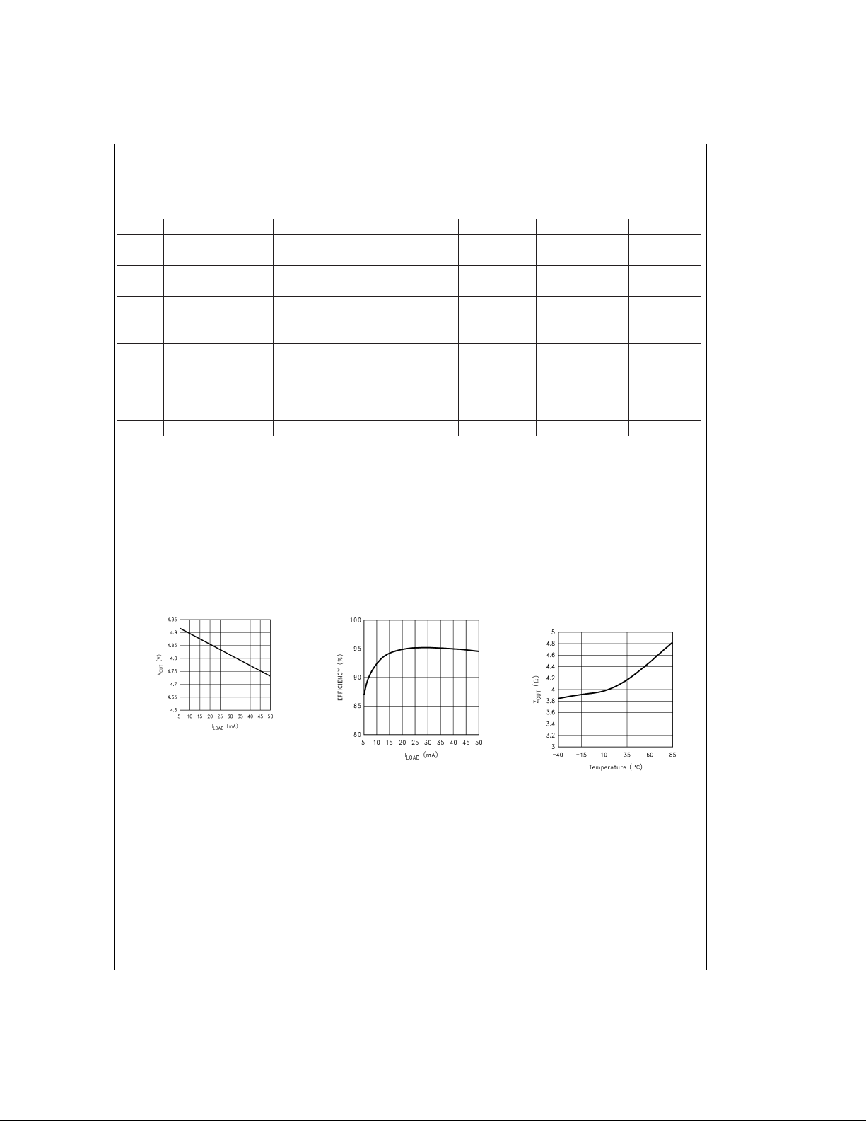
Typical Performance Characteristics
V
vs I
load
(Step-Up)
DS100146-4
out
Pηvs I
load
(Step-Up)
DS100146-5
Output Source Impedance vs
Temperature (Step-Up)
DS100146-6
www.national.com3
Page 4

Typical Performance Characteristics (Continued)
LM3351
V
vs I
out
(Step-Down)
load
Pηvs I
(Step-Down)
load
Output Source Impedance vs
Temperature (Step-Down)
DS100146-7
Switching Frequency vs
Temperature
DS100146-10
Pin Description
Pin Name Function
1 Cap1+ Positive terminal for the first charge
2 Cap1− Negative terminal for the first charge
3 Cap2+ Positive terminal for the second charge
4 Cap2− Negative terminal for the second charge
5V
6 Gnd Ground
7V
8 Enable Active high CMOS logic level Enable
pump capacitor.
pump capacitor.
pump capacitor.
pump capacitor.
In Step-Up mode, this will be the input
low
terminal. In Step-Down mode, this will
be the output terminal.
In Step-Down mode, this will be the
high
input terminal. In Step-Up mode, this
will be the output terminal.
Input. Connect to Voltage Input terminal
to enable the IC. Connect to Ground
(Pin 6) to disable.
DS100146-8
DS100146-9
Detailed Operation
OPERATING PRINCIPLE
The LM3351 is a charge-pump voltage converter that provides a voltage conversion ratio of 3/2 in step-up mode and
a conversion ratio of 2/3 in the step-down mode. Thus it can
be used in the step-down mode to provide a 3.3V output
from a regulated 5V input or in the step-up mode to provide
a 5V output from a regulated 3.3V input. Other values of input voltages can be used as long as they are within the limits.
The LM3351 contains an array of CMOS switches which are
operated in a certain sequence to provide the step-up or
step-down of the input supply. An internal RC oscillator provides the timing signals.
Energy transfer and storage are provided by four inexpensive ceramic capacitors. The selection of these capacitors is
explained in the Capacitor Selection section under Application Information.
www.national.com 4
Page 5

Detailed Operation (Continued)
STEP-UP APPLICATIONS NEED AN EXTRA DIODE
The LM3351 is biased from pin V
cations, an external Schottky diode (D1) is needed to supply
power to V
shutdown, this diode will provide a DC path from V
during startup (See
high
The load may therefore continue to draw current from the in-
. Thus for step-up appli-
high
Figure 1
). Note that during
in
to V
out
put voltage source. This Schottky diode is not required for
step-down applications (See
Figure 2
).
SHUTDOWN MODE
When ENABLE is a logic low (ground), the LM3351 enters a
low power shutdown mode. In this mode, all circuitry is disabled and therefore, all switching action stops. During shutdown, the current consumption drops to 250 nA (typical).
When ENABLE is a logic high, (i.e. 3.3V for step-up mode
and 5.0V for step-down mode), the LM3351 returns to normal operation.
Application Information
CAPACITOR SELECTION
The LM3351 requires four capacitors: an input bypass capacitor (connected between V
capacitor (connected between V
sampling capacitors (C1 and C2 in
±
(
20%) ceramic chip type capacitors are recommended for
all four capacitors. The usable operating frequency should
be greater than 5 MHz for all capacitors.
The output hold capacitor value determines the output ripple.
Increasing the value of the hold capacitor decreases the
ripple. The value of this capacitor (C
(approximately) based on the output ripple (∆V
ments from:
and ground), an output hold
in
and ground), and two
out
Figures 1, 2
) can be calculated
out
). 1.0 µF
) require-
out
LM3351
.
where I
quency.
is the load current and fOis the oscillator fre-
load
In order to ensure superior performance over the entireoperating temperature range, capacitors made of X7R dielectric
material are suggested. However, capacitors made of other
dielectric materials that still meet the
±
20%specification
over the entire temperature range can also be used.
PRECAUTIONS
The LM3351 is not short circuit protected.
www.national.com5
Page 6

Typical Application Circuits
LM3351
Layout Information
DS100146-12
FIGURE 1. Step-Up Converter
DS100146-13
FIGURE 2. Step-Down Converter
LAYOUT CONSIDERATIONS
Figure 3
The LM3351’s high switching frequency (200 kHz) makes a good layout important.
illustrates a typical layout. It is important to keep the distance short between the four capacitors and the IC. Wide traces and grounding are also recommended.
These steps will minimize trace inductance and high frequency ringing. Of the four capacitors, C
value of di/dt. It is therefore most important to keep them close to the IC. The ground lead that C
be kept wide and short.
IN
IN
and C
and C
have the highest
OUT
share should also
OUT
The location of the diode (D1) used in the step-up configuration is not critical. This diode is only used during the initial turn on of
the IC. D1 is not needed in step-down applications.
www.national.com 6
Page 7

Layout Information (Continued)
A. Copper side (5X)
LM3351
DS100146-15
B. Actual Size of the Layout
DS100146-14
C. Copper side with Component Locations (5X)
FIGURE 3. Typical Layout
DS100146-16
www.national.com7
Page 8

Physical Dimensions inches (millimeters) unless otherwise noted
LM3351 Switched Capacitor Voltage Converter
Order Number LM3351MMX or LM3351MM
8-Lead Mini SO (MM)
NS Package Number MUA08A
LIFE SUPPORT POLICY
NATIONAL’S PRODUCTS ARE NOT AUTHORIZED FOR USE AS CRITICAL COMPONENTS IN LIFE SUPPORT
DEVICES OR SYSTEMS WITHOUT THE EXPRESS WRITTEN APPROVAL OF THE PRESIDENT AND GENERAL
COUNSEL OF NATIONAL SEMICONDUCTOR CORPORATION. As used herein:
1. Life support devices or systems are devices or
systems which, (a) are intended for surgical implant
into the body, or (b) support or sustain life, and
whose failure to perform when properly used in
accordance with instructions for use provided in the
2. A critical component is any component of a life
support device or system whose failure to perform
can be reasonably expected to cause the failure of
the life support device or system, or to affect its
safety or effectiveness.
labeling, can be reasonably expected to result in a
significant injury to the user.
National Semiconductor
Corporation
Americas
Tel: 1-800-272-9959
Fax: 1-800-737-7018
Email: support@nsc.com
www.national.com
National does not assume any responsibility for use of any circuitry described, no circuit patent licenses are implied and National reserves the right at any time without notice to change said circuitry and specifications.
National Semiconductor
Europe
Fax: +49 (0) 1 80-530 85 86
Email: europe.support@nsc.com
Deutsch Tel: +49 (0) 1 80-530 85 85
English Tel: +49 (0) 1 80-532 78 32
Français Tel: +49 (0) 1 80-532 93 58
Italiano Tel: +49 (0) 1 80-534 16 80
National Semiconductor
Asia Pacific Customer
Response Group
Tel: 65-2544466
Fax: 65-2504466
Email: sea.support@nsc.com
National Semiconductor
Japan Ltd.
Tel: 81-3-5639-7560
Fax: 81-3-5639-7507
 Loading...