

Page 1
现货库存、技术资料、百科信息、热点资讯,精彩尽在鼎好!
LM2901,LM339/LM339A,LM3302
LM239/LM239A
Quad Comparator
www.fairchildsemi.com
Features
• Single or Dual Supply Operation
• Wide Range of Supply Voltage
LM2901,LM339/LM339A,LM239/LM239A: 2 ~ 36V
(or ±1 ~ ±18V)
LM3302: 2 ~ 28V (or ±1 ~ ±14V)
• Low Supply Current Drain 800µA Typ.
• Open Collector Outputs for Wired and Connecto r s
• Low Input Bia s Current 25 nA Typ.
• Low Input Offset Current ±2.3nA Typ.
• Low Input Offset Voltage ±1.4mV T yp .
• Input Common Mode Voltage Range Includes Ground.
• Low Output Satura ti on Voltage
• Output Compatible With TTL, DTL and MOS Logic
System
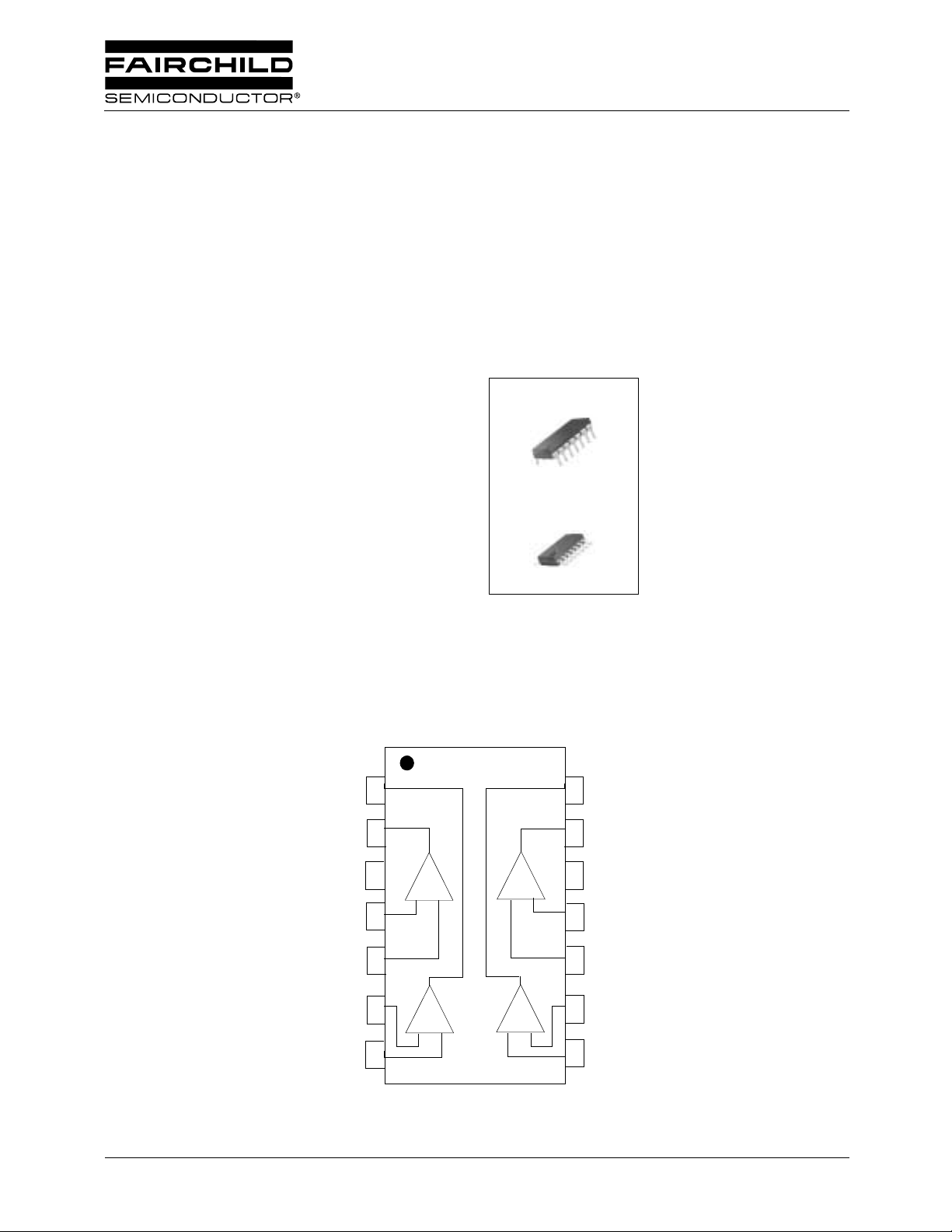
Internal Block Diagram
Description
The LM2901, LM3 39/LM339A ,LM239/LM239A, LM3302
consist of four independent voltage comparators designed
to operate from single power supply over a wide voltage
range.
14-DIP
1
14-SOP
1
©2002 Fairchild Semiconductor Corporation
OUT2
OUT1
V
CC
IN1(-)
IN1(+)
IN2(-)
IN2(+)
14
13
12
11
10
9
8
OUT3
OUT4
GND
IN4(+)
IN4(-)
IN3(+)
IN3(-)
1
2
3
+
-
4
5
6
7
+
-
+
-
+
-
Rev. 1.0.2
Page 2
LM2901,LM339/LM339A,LM3 302 L M23 9/LM 239A
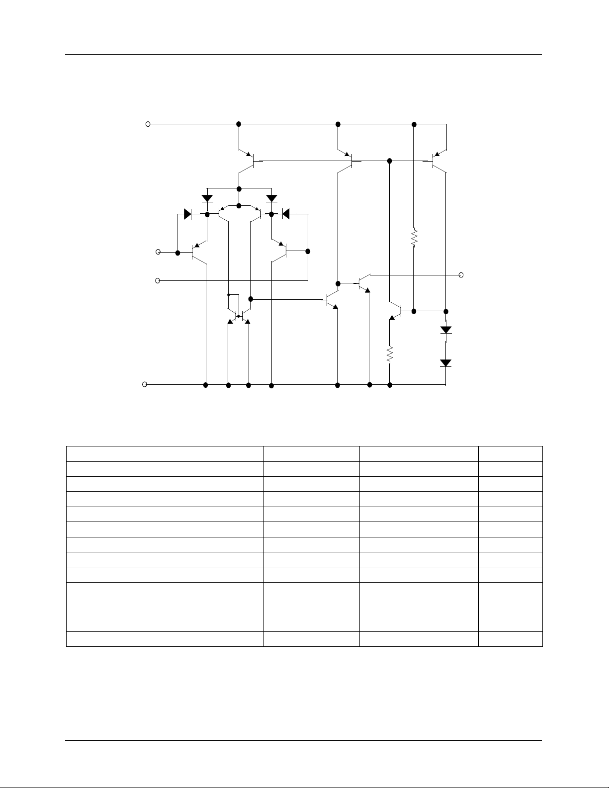
Schematic Diagram
V
CC
D2
Q2
D1
IN(+)
IN(-)
GND
Q1
Q5
Absolute Maximum Ratings
Q9
Q3
Q6
D3
Q4
D4
Q12
Q7
Q8
Q13
R1
Q14
R2
OUTPUT
D5
D6
Parameter Symbol Value Unit
Supply Voltage V
Supply Voltage only LM3302 V
Differential Input Voltage V
Differential Input Voltage Only LM3302 V
I(DIFF)
I(DIFF)
Input Voltage V
Input Voltage Only LM3302 V
CC
CC
I
I
±18 or 36 V
±14 or 28 V
36 V
28 V
-0.3 to +36 V
-0.3 to +28 V
Output Short Circuit to GND - Continuous Power Dissipation P
D
570 mW
Operating Temperature
LM339/LM339A
LM2901/LM3302
LM239/LM239A
Storage Temperature T
T
OPR
STG
0 ~ +70
-40 ~ +85
-25 ~ +85
-65 ~ +150 °C
°C
2
Page 3
Electrical Characteristics
(VCC = 5V, TA = 25°C, unless otherwise specified)
LM2901,LM339/LM339A,LM33 02 LM239/LM239A
Parameter Symbol Conditions
V
=1.4V, RS = 0Ω -1 2 -1.45mV
Input Offset
Voltage
V
Input Offset
Current
Input Bias Current I
BIAS
Input Common
Mode Voltage
V
Range
Supply Current I
Voltage Gain G
Large Signal
Response Time
T
LRES
Response Time T
Output Sink
Current
Output Saturation
Voltage
Output Leakage
Current
Differential Voltage V
I
SINK
V
I
o(LKG)
I(DIFF)
IO
I
IO
I(R)
CC
V
RES
SAT
O(P)
Note1 - - 4.0 - - 9.0
I
- I
IN(+)
IN(-)
, V
CM
Note1 - - 150 - - 150
V
= 0V - 57 250 - 57 250
CM
Note1 - - 400 - - 400
V
= 30V 0 - VCC-1.5 0 - VCC-1.5
CC
Note1 0 - VCC-2 0 - VCC-2
VCC = 5V, RL = ∞ - 1.1 2.0 - 1.1 2.0 mA
VCC =15V, R
≥ 15kΩ
L
(for large swing)
VI = TTL Logic Swing
V
= 1.4V, VRL = 5V,
REF
R
= 5.1kΩ (Note2)
L
VRL = 5V, RL = 5.1kΩ
(Note2)
V
≥ 1V, V
I(-)
V
≤ 1.5V
O(P)
V
≥ 1V, V
I(-)
= 4mA Note1 - - 700 - - 700
I
SINK
V
= 0V
I(-)
V
= 1V
I(+)
= 0V,
I(+)
= 0V - 140 400 - 140 400
I(+)
V
O(P)
V
O(P)
Note1 - - 36 - - 36 V
LM239A/LM339A LM239/LM339
Min. Typ. Max. Min. Typ. Max.
Unit
= 0V - 2.3 50 - 2.3 50 nA
nA
V
50 200 - 50 200 - V/mV
- 300 - - 300 - ns
-1.3 - -1.3- µs
618 - 618- mA
mV
= 5V - 0.1 - - 0.1 - nA
= 30V - - 1.0 - - 1.0 µA
Note:
1. LM339/LM339A : 0 ≤ T
LM2901/LM3302 : -40 ≤ T
LM239/LM239A : -25 ≤ T
2. These parameters, although guaranteed, are not 100% tested in production.
≤ +70°C
A
A
≤ +85°C
A
≤ +85°C
3
Page 4

LM2901,LM339/LM339A,LM3 302 L M23 9/LM 239A
Electrical Characteristics
(Continued)
(VCC = 5V, TA = 25°C, unless otherwise specified)
Parameter Symbol Conditions
V
=1.4V, RS = 0Ω -27-220
Input Offset Voltage V
Input Offset Current I
Input Bias Current I
Input Common
Mode Voltage
V
Range
IO
IO
BIAS
I(R)
O(P)
Note1 - 9 15 - - 40
Note1 - 50 200 - - 300
Note1 - 200 500 - - 1000
LM2901, VCC =30V
LM3302, V
CC
=28V
Note1 0 -
RL =∞, VCC=5V - 1.1 2.0 - 1.1 2.0
Supply Current I
Voltage Gain G
Large Signal
Response Time
CC
V
T
LRESVI
=∞,VCC=30V
R
L
(LM3302, V
VCC =15V, R
CC
L
=28V)
≥ 15kΩ
(for large swing)
=TTL Logic Swing
V
=1.4V, VRL =5V, RL =5.1kΩ
REF
(Note2)
Response Time T
Output Sink Current I
Output Saturation
Voltage
Output Leakage
Current
I
Differential Voltage V
RESVRL
SINKVI(-)
V
SAT
O(LKG)
I(DIFF)
= 5V, RL = 5.1kΩ (Note2) - 1.3 - - 1.3 - µs
≥ 1V, V
V
≥ 1V, V
I(-)
=4mA Note1 - - 700 - - 700
I
SINK
V
= 0V
I(-)
V
= 1V
I(+)
=0V, V
I(+)
= 0V - 140 400 - 140 400
I(+)
V
V
Note1 - -36- -28V
LM2901 LM3302
Min. Typ. Max. Min. Typ. Max.
- 2.3 50 - 3 100
- 57 250 - 57 250 nA
V
0-
CC
-1.5
V
CC
-2
0-
0-
- 1.6 2.5 - 1.6 2.5
25 100 - 2 30 -
- 300 - - 300 -
≤ 1.5V 6 18 - 6 18 - mA
O(P)
= 5V - 0.1 - - 0.1 - nA
O(P)
= 30V - - 1.0 - - 1.0 µA
O(P)
V
CC
-1.5
V
CC
-2
Unit
mV
nA
V
mA
V/
mV
ns
mV
Note:
1. LM339/LM339A : 0 ≤ T
LM2901/LM3302 : -40 ≤ T
LM239/LM239A : -25 ≤ T
2. These parameters, although guaranteed, are not 100% tested in production.
≤ +70°C
A
A
≤ +85°C
A
≤ +85°C
4
Page 5

Typical Performance Characteristics
Figure 1. Supply Current vs Supply Voltage Figure 2. Input Current vs Supply Voltage
LM2901,LM339/LM339A,LM33 02 LM239/LM239A
Figure 3. Output Saturation Voltage vs Sink Current Figure 4. Response Time for Various In put
Figure 5. Response Time for Various Input
Overdrive-Positive Transition
Overdrive-Negative Tr ansition
5
Page 6

LM2901,LM339/LM339A,LM3 302 L M23 9/LM 239A
Mechanical Dimensions
Package
6.40
±0.20
0.252
±0.008
14-DIP
Dimensions in millimeters
2.08
0.082
()
#1
#7
7.62
0.300
#14
#8
MAX
19.80
0.780
0.200
3.25
0.128
5.08
±0.20
±0.008
19.40
0.764
±0.20
±0.008
MAX
0.20
0.008
3.30
0.130
±0.10
0.46
2.54
MIN
±0.30
±0.012
±0.004
0.018
0.100
±0.10
1.50
±0.004
0.059
+0.10
0.25
–0.05
+0.004
0.010
0~15°
–0.002
6
Page 7

LM2901,LM339/LM339A,LM33 02 LM239/LM239A
Mechanical Dimensions
Package
#1
(Continued)
14-SOP
#14
1.55 ±0.10
0.061 ±0.004
MAX
8.70
0.343
8.56 ±0.20
Dimensions in millimeters
0.05
MIN
0.002
0.47
0.019
()
0.004
+0.10
-0.05
+
-0.002
0.337 ±0.008
0.406
0.016
0.10
0.004
+
-0.05
+
-0.002
0.20
0.008
0.60 ±0.20
0.024 ±0.008
#7
6.00 ±0.30
0.236 ±0.012
3.95 ±0.20
0.156 ±0.008
5.72
0.225
#8
0~8°
1.80
0.071
MAX
MAX0.10
MAX0.004
1.27
0.050
7
Page 8

LM2901,LM339/LM339A,LM3 302 L M23 9/LM 239A
Ordering Information
Product Number Package Operating Temperature
LM339N
LM339AN
LM339M
LM339AM
LM2901N 14-DIP
LM2901M 14-SOP
LM3302N 14-DIP
LM3302M 14-SOP
LM239N
LM239AN
LM239M
LM239AM
14-DIP
0 ~ +70°C
14-SOP
-40 ~ +85°C
14-DIP
-25 ~ +85°C
14-SOP
DISCLAIMER
FAIRCHILD SEMICONDUCTOR RESERVES THE RIGHT TO MAKE CHANGES WITHOUT FURT HER NOTICE TO ANY
PRODUCTS HEREI N TO IMPROVE RELIABILITY, FUNCTIO N OR DESIGN. FAIRCH IL D DOES NOT ASSUME ANY
LIABILITY ARISING OUT OF THE APPLICATION OR USE OF ANY PRODUCT OR CIRCUIT DESCRIBED HEREIN; NEITHER
DOES IT CONVEY ANY LICENSE UNDER IT S PATENT RIGHTS, NOR THE RIGHTS OF OTHE RS.
LIFE SUPPORT POL I CY
FAIRCHILD’S PR ODUCTS ARE NOT AUTH ORIZED FOR USE AS C RITICAL COMPONENT S IN LIFE SUPPORT DE VICES
OR SYSTEMS WITHOUT THE EXPRESS WRITTEN APPROVAL OF THE PRESIDENT OF FAIRCHILD SEMICONDUCTOR
CORPORATION. As used herein :
1. Life support devices or systems are devices or systems
which, (a) are intended for surgical implant into the body,
or (b) support or sustain life, and (c) whose failure to
perform when properly used in accordance with
instructions for use provided in the labeling, can be
reasonably expected to result in a significant injury of the
user.
www.fairchildsemi.com
2. A critical component in any component of a life support
device or sy stem whose fai lure to perform can be
reasonably expec ted to cause the failur e of the life support
device or system, or to affect its safety or effec t iv ene ss .
11/19/02 0.0m 001
2002 Fairchild Semiconductor Corporation
Stock#DSxxxxxxxx
 Loading...