

Page 1
现货库存、技术资料、百科信息、热点资讯,精彩尽在鼎好!
UNISONIC TECHNOLOGIES CO.,
LM324
QUAD OPERATIONAL
AMPLIFIERS
DESCRIPTION
The UTC LM324 consists of four independent, high gain
internally frequency compensated operational amplifiers which are
designed specifically to operated from a single power supply over a
wide voltage range. Operation from split power supplies is also
possible. Application areas include transducer amplifier, DC gain
blocks and all the conventional OP amp circuits which now can be
easily implemented in single power supply system.
FEATURES
*Internally frequency compensated for unity gain.
*Large DC voltage gain :100dB.
*Wide operating supply range (Vcc=3V~32V).
*Input common-mode voltage includes ground.
*Large output voltage swing: From 0V to Vcc-1.5V.
*Power drain suitable for battery operation.
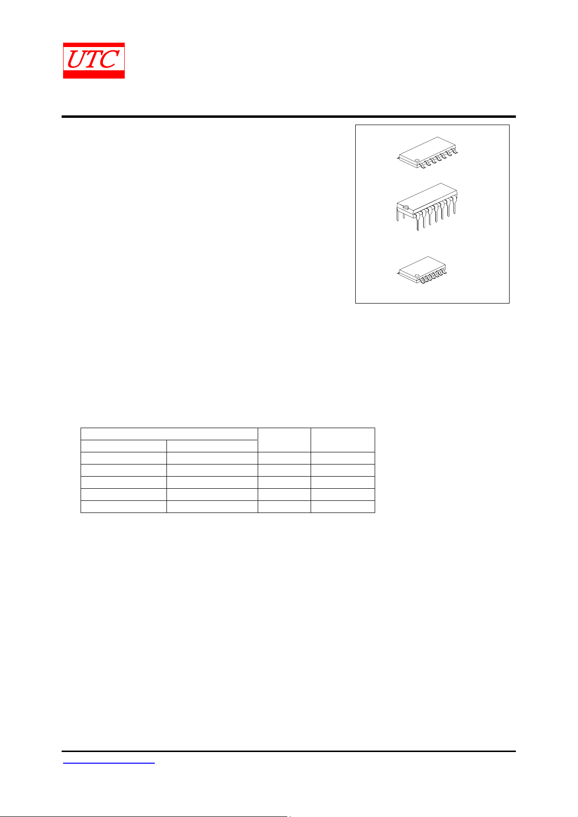
LINEAR INTEGRATED CIRCUIT
SOP-14
DIP-14
TSSOP-14
*Pb-free plating product number: LM324L
ORDERING INFORMATION
Ordering Number
Normal Lead Free Plating
Package Packing
LM324-P14-R LM324L-P14-R TSSOP-14 Tape Reel
LM324-P14-T LM324L-P14-T TSSOP-14 Tube
LM324-S14-R LM324L-S14-R SOP-14 Tape Reel
LM324-S14-T LM324L-S14-T SOP-14 Tube
LM324-D14-T LM324L-D14-T DIP-14 Tube
www.unisonic.com.tw 1
Copyright © 2005 Unisonic Technologies Co.,
QW-R105-006,D
Page 2
LM324 LINEAR INTEGRATED CIRCUIT
PIN DESCRIPTION
BLOCK DIAGRAM
Only one section
OUT 1
IN 1(-)
IN 1(+)
IN 2(+)
IN 2(-)
OUT 2
1
2
3
4
Vcc GND
5
6
7
14
13
12
11
10
9
8
OUT 4
IN 4(-)
IN 4(+)
IN 3(+)
IN 3(-)
OUT 3
Vcc
IN (-)
IN (+)
UNISONIC TECHNOLOGIES CO., LTD 2
www.unisonic.com.tw
Output
GND
QW-R105-006,D
Page 3

LM324 LINEAR INTEGRATED CIRCUIT
ABSOLUTE MAXIMUM RATINGS
PARAMETER SYMBOL RATINGS UNIT
Supply Voltage V
Differential Input Voltage V
CC
32 V
I(DIFF)
Input Voltage VI -0.3 ~ +32 V
Power Dissipation PD 570 mW
Operating Temperature Range T
Storage Temperature Range T
0 ~ +70 °C
OPR
-40 ~ +150 °C
STG
ELECTRICAL CHARACTERISTICS
(VCC=5.0V, All voltage referenced to GND unless otherwise specified.)
PARAMETER SYMBOL TEST CONDITIONS MIN TYP MAX UNIT
V
=0V toVCC-1.5V
Input Offset Voltage VIO
CM
V
=1.4V, RS=0Ω
O(P)
Input Offset Current IIO 50 nA
Input Bias Current I
Input Common Mode Voltage V
Power Supply Current ICC
Large Signal Voltage Gain GV
Output Voltage Swing
250 nA
BIAS
VCC=30V 0 VCC-1.5 V
I(R)
RL=∝, VCC=30V 1.0 3.0 mA
=5V 0.7 1.2 mA
V
CC
V
=15V, RL≧2KΩ
CC
=1V ~ 11V
V
O(P)
V
O(H)
V
O(L)
VCC=30V, RL=2KΩ 26 V
=30V, RL=10KΩ 27 28 V
V
CC
VCC=5V, RL>10KΩ 5 20 mV
Common Mode Rejection Ratio CMRR 65 75 dB
Power Supply Rejection Ratio PSRR 65 100 dB
Channel Separation CS f=1KHZ ~ 20KHZ 120 dB
Short Circuit Current to Ground ISC 40 60 mA
V
(+)=1V, VI(-)=0V
I
V
CC
V
(+)=0V, VI(-)=1V
I
V
CC
V
(+)=0V, VI(-)=1V
I
V
CC
=15V, V
=15V, VO(P)=2V
=15V, V
=2V
O(P)
=200mV
O(P)
V
Output Current
Differential Input Voltage V
I
SOURCE
I
SINK
I(DIFF)
±18
V
7.0 mV
25 100 V/mV
20 40 mA
10 13 mA
12 45 mA
V
CC
UNISONIC TECHNOLOGIES CO., LTD 3
www.unisonic.com.tw
QW-R105-006,D
Page 4

LM324 LINEAR INTEGRATED CIRCUIT
TYPICAL CHARACTERISTICS
Fig. 1 Input Voltage Range
15
10
5
Input voltgae (¡ÀV)
0
05
Supply Voltage (+- Vdc)
Fig.3 S upp ly Current
40
3
2
Ta=0~+85¢XC
Positive
Negative
10
Vcc
Fig.2 I np ut C urrent
100
80
60
40
Input current (nA)
20
15
0
-50 -25 0 25 50 75 100
Vcc=+30V
Vcc=+15V
Vcc=+5V
Temperature (¢XC)
Fig.4 Voltage Ga i n
160
Ic
120
80
RL=20kΩ
RL=2kΩ
1
Supply Current (mA)
0
010 203040
Ta=-40¢XC
Supply Voltage (V)
120
100
80
60
40
Voltage Gain (dB)
20
0
Fig.5 Open Loop F requency re spons e
Vcc=15V
01
10
10210310410
Vcc
0.1µF
Vin
Vcc/2
5
10610710
100MΩ
Vcc=30V
Frequency (Hz)
Voltgae Gain (dB)
40
0
0 7.5 15 22.5 30
Supply Voltage (V)
120
Fig.6 Com mon-mode reje c t i on R a t io
100
Vcc=+7.5V
100 kΩ
Vee=-7.5V
5
10
6
10
80
60
CMRR (dB)
40
20
0
+7.5V
100 Ω
100 Ω
Vin
100kΩ
-7.5V
2
10
3
10
4
10
Frequency (Hz)
UNISONIC TECHNOLOGIES CO., LTD 4
www.unisonic.com.tw
QW-R105-006,D
Page 5

LM324 LINEAR INTEGRATED CIRCUIT
TYPICAL CHARACTERISTICS(cont.)
3
2
1
Input Voltage (V)Output Voltage (V)
0
3
2
1
0
010
Fig. 9 Lar ge signal F requency Re sponse
15
10
Fig.7
RL=2kΩ
Vcc=15V
20 30 40
Time (µs)
+15V
100k
1k
Vi
+7V
Fig.8 Voltage Follower pulse response
(small signal)
450
400
350
Output voltgae (V)
300
275
50
0123456789
Time (µs)
Fig.10 Output Characteristics
current sourcing
8
7
Ta=25¢XC
6
2k
5
4
Vcc/2
Vcc
Vo
Io
5
Output swin g (Vp-p)
0
35
4
1010
10
6
10
Frequency (Hz)
Fig.11 Output Characteristic s Current sinking
10
1
Vcc=+5V
Vcc=+15V
-1
10
Output Voltage (V)
Vcc=+30V
-3
10
-2
10
-1
10
Output Sink Cur rent ( m A)
110210
Vcc/2
Vcc
Vo
Io
3
Output refference Vcc (V)
2
1
10
-2
-3
10
-1
10
10
2
101
Output Source current (mA)
Fig. 12 Curr e nt L i miting
60
40
Output Current (mA)
20
0
-50 -25
0
25 50 75 100
Temperatur e (¢XC)
UNISONIC TECHNOLOGIES CO., LTD 5
www.unisonic.com.tw
QW-R105-006,D
Page 6

LM324 LINEAR INTEGRATED CIRCUIT
UTC assumes no responsibility for equipment f ailures that result from using product s at val ues that
exceed, even momentarily, rated values (such as maximum ratings, operating condition ranges, or
other parameter s) listed in product s specifi cations of any and all UT C products described or contai ned
herein. UTC products are not designed for use in l ife support appli ances, devices or system s where
malf uncti on of these products can be reasonably expect ed to result in personal i njury. Reproduct ion in
whole or in part is prohibi ted without the prior writ ten consent of the copyri ght owner. The inf ormation
presented in thi s document does not f orm part of any quotati on or contract, is beli ev ed to be accurate
and reliable and may be changed without notice.
UNISONIC TECHNOLOGIES CO., LTD 6
www.unisonic.com.tw
QW-R105-006,D
 Loading...