

Datasheet LM317P, LM317K, LM317D2T, LM217T, LM217K Datasheet (SGS Thomson Microelectronics)
...Page 1
LM117/217
LM317
1.2V TO 37V VOLTAGE REGULATOR
November 1999
■ OUTPUT VOLTAGERANGE: 1.2TO 37V
■ OUTPUT CURRENT INEXCESS OF 1.5A
■ 0.1%LINE AND LOADREGULATION
■ FLOATINGOPERATION FOR HIGH
VOLTAGES
■ COMPLETESERIESOF PROTECTIONS:
CURRENTLIMITING,THERMAL
SHUTDOWNANDSOA CONTROL
DESCRIPTION
The LM117/LM217/LM317 are monolithic
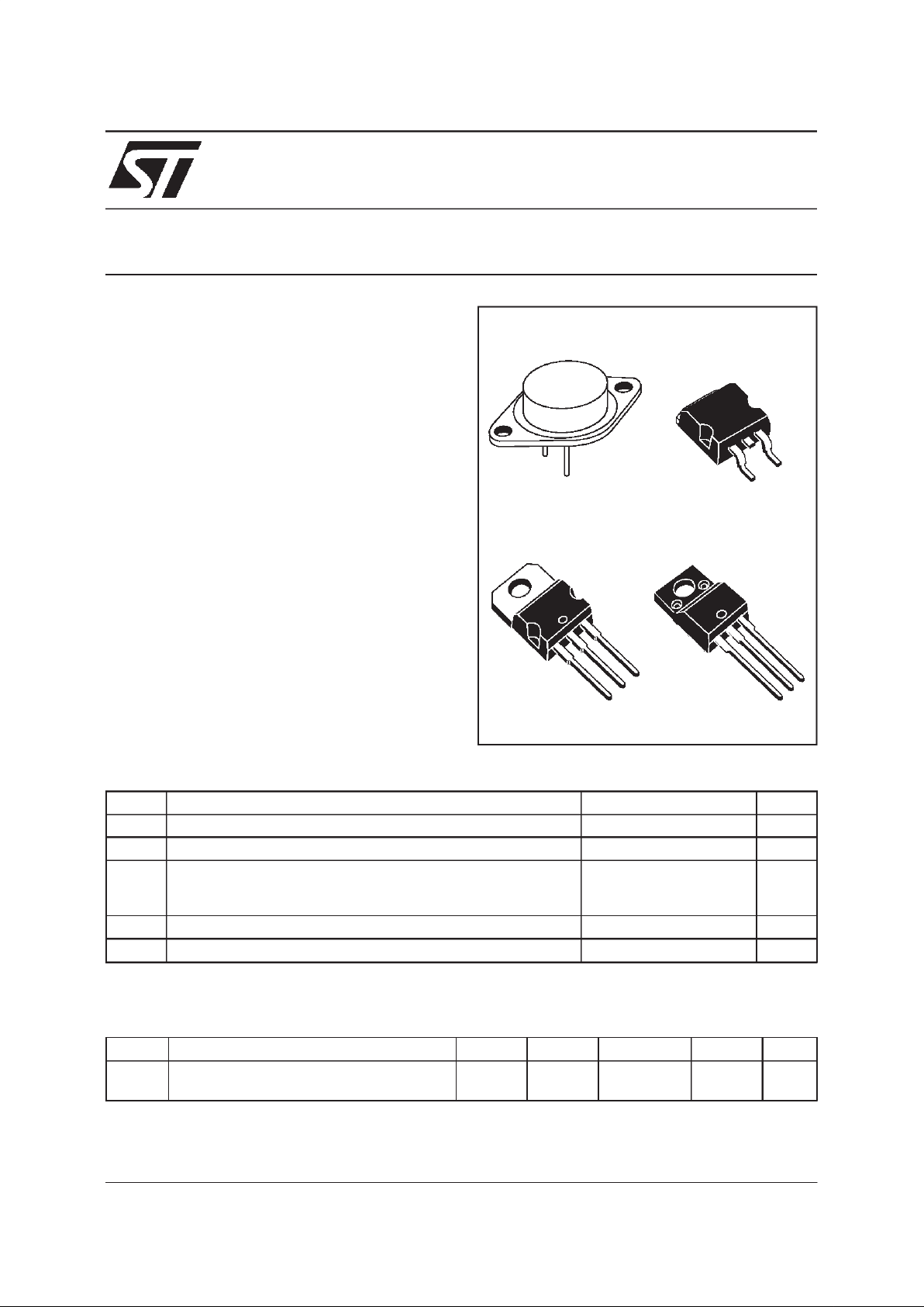
integrated circuit in TO-220, ISOWATT220, TO-3
and D
2
PAK packages intended for use as
positiveadjustable voltageregulators.
They are designed to supply more than 1.5A of
load current with an output voltage adjustable
overa 1.2 to 37V range.
The nominal output voltage is selected by means
of only a resistive divider, making the device
exceptionally easy to use and eliminating the
stockingof manyfixed regulators.
TO-3
TO-220
D
2
PAK
ABSOLUTE MAXIMUMRATING
Symbol Parameter Value Unit
V
i-o
Input-output Differential Voltage 40 V
I
O
OutputCurrent Intenrally Limited
T
op
OperatingJunction Temperaturefor:LM117
LM217
LM317
-55 to 150
-25 to 150
0 to 125
o
C
o
C
o
C
P
tot
PowerDissipation Internally Limited
T
stg
StorageTemperature - 65 to 150
o
C
THERMALDATA
Symbol Parameter TO-3 TO-220 ISOWATT220 D2PAK Unit
R
thj-cas e
R
thj-amb
Thermal Resistance Junction-case Max
Thermal Resistance Junction-ambient Max
4
35
3
50
4
60
3
62.5
o
C/W
o
C/W
ISOWATT220
1/11
Page 2
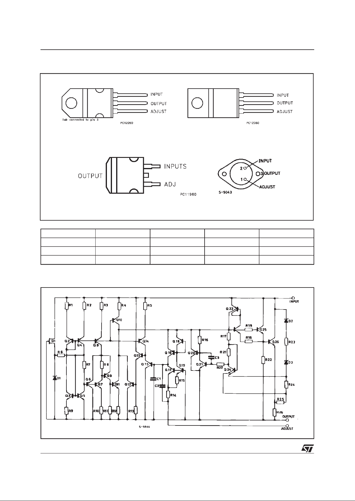
CONNECTION DIAGRAM ANDORDERING NUMBERS
(top view)
TO-220
D
2
PAK TO-3
Type TO-3 TO-220 ISOWATT220 D
2
PAK
LM117 LM117K
LM217 LM217K LM217T LM217D2T
LM317 LM317K LM317T LM317P LM317D2T
SCHEMATIC DIAGRAM
ISOWATT220
LM117/217/317
2/11
Page 3
BASIC ADJUSTABLE REGULATOR
ELECTRICAL CHARACTERISTICS (V
i-Vo
= 5V, Io=500 mA, I
MAX
= 1.5Aand P
MAX
= 20W,unless
otherwisespecified)
Symbol Parameter Test Conditions LM117/LM217 LM317 Unit
Min. Typ. Max. Min. Typ. Max.
∆V
o
LineRegulation Vi-Vo= 3 to40 V Tj=25oC 0.01 0.02 0.01 0.04 %/V
0.02 0.05 0 . 02 0. 07 %/V
∆V
o
LoadRegulation
V
o
≤ 5V
I
o
=10mAtoI
MAX
Tj=25oC515 525mV
20 50 20 70 mV
V
o
≥
5V
I
o
=10mAtoI
MAX
Tj=25oC 0.1 0.3 0.1 0 .5 %
0.3 1 0.3 1.5 %
I
ADJ
Adjustment Pin Current 50 100 50 100
µ
A
∆
I
ADJ
Adjustment Pin Current Vi-Vo= 2.5 to 40V
I
o
=10mAtoI
MAX
0.2 5 0.2 5
µ
A
V
REF
Reference Voltage
(between pin3 andpin
1)
Vi-Vo= 2.5 to 40V
I
o
=10mAtoI
MAX
P
D
≤
P
MAX
1.21.251.3 1.21.251.3 V
∆
V
o
V
o
OutputVoltage
Temperature Stability
11%
I
o(min)
MinimumLoad Current Vi-Vo= 40V 3.5 5 3.5 10 mA
I
o(max)
Maximum Load
Current
V
i-Vo
≤
15 V
P
D<PMAX
1.52.2 1.52.2 A
V
i-Vo
=40V
P
D<PMAX
Tj=25oC
0.4 0.4 A
e
N
OutputNoise Voltage
(percentance of V
O
)
B= 10Hz to 10KHz
Tj=25oC
0.003 0.003 %
SVR Supply Voltage
Rejection(*)
T
j
=25oC
f =120 Hz
C
ADJ
=0 65 65 dB
C
ADJ
=10µF
66 80 66 80 dB
(*) CADJ is connected between pin 1 and ground.
Note:
(1) Unless otherwisespecified the above specs, apply over the following conditions :LM 117 T
j
= –55 to 150°C;
LM 217 T
j
= –25 to 150°C ; LM317 Tj= 0to 125°C.
LM117/217/317
3/11
Page 4
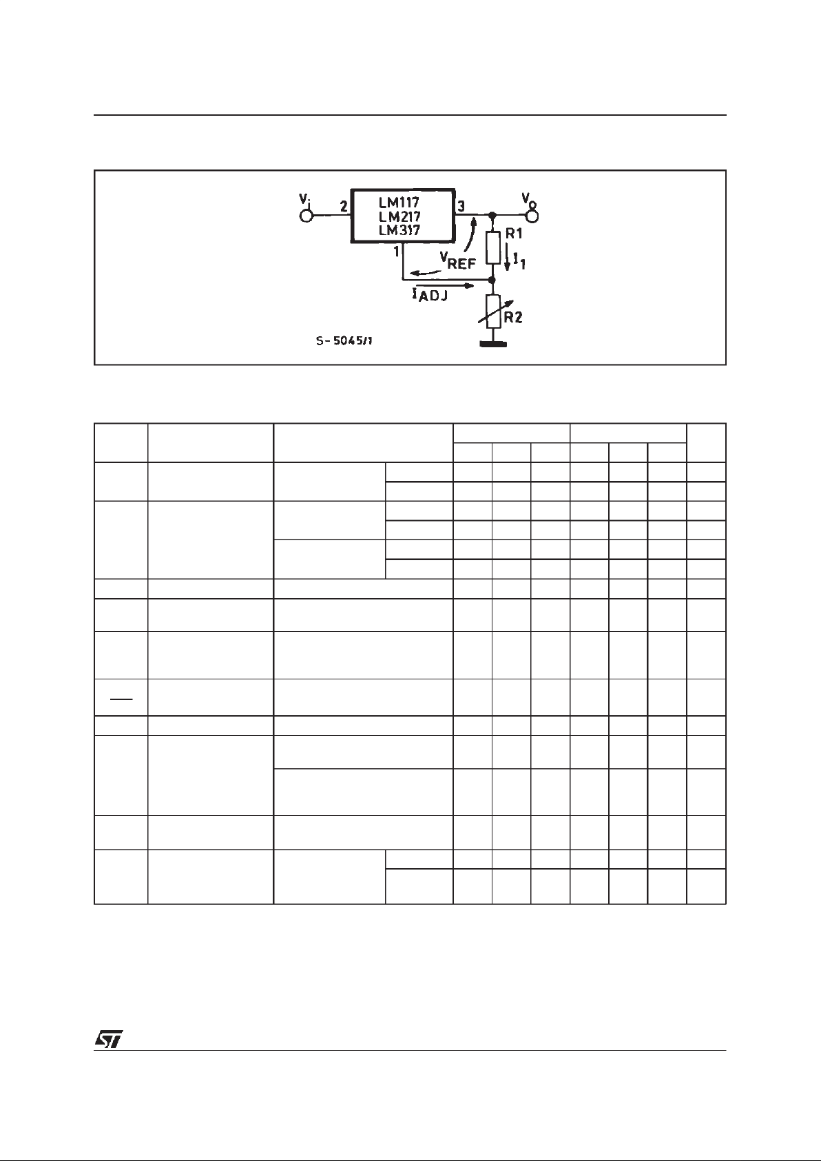
APPLICATION INFORMATION
The LM117/217/317 provides an internal
reference voltage of 1.25V between the output
and adjustments terminals. This is used to set a
constant current flow across an external resistor
divider(see fig. 4),giving an outputvoltage V
O
of:
V
O=VREF
(1 +
R
2
R
1
) +I
ADJR2
The device was designed to minimize the term
I
ADJ
(100µA max) and to maintainit very constant
with line and load changes. Usually, the error
term I
ADJ
⋅ R2can be neglected. To obtain the
previous requirement, all the regulator quiescent
current is returned to the output terminal,
imposinga minimum load current condition.If the
load is insufficient, the output voltagewill rise.
Since the LM117/217317 is a floating regulator
and ”sees” only the input-to-output differential
voltage,supplies of very highvoltage withrespect
to ground can be regulated as long as the
maximum input-to-output differential is not
exceeded. Furthermore, programmable regulator
are easily obtainable and, by connecting a fixed
resistor between the adjustment and output, the
device can be used as a precision current
regulator.
In order to optimise the load regulation, the
current set resistor R1 (see fig. 4) should be tied
as close as possible to the regulator, while the
ground terminal of R2 should be near the ground
of theload to provideremote ground sensing.
Performance may be improved with added
capacitanceas follow:
Aninput bypass capacitorof 0.1µF
An adjustment terminal to ground 10µF capacitor
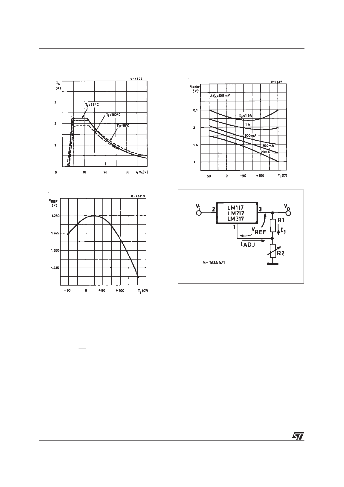
Figure4 : Basic AdjustableRegulator.
Figure1 :
OutputCurrent vs. Input-output
DifferentialVoltage.
Figure2 :
DropoutVoltage vs. Junction
Temperature.
Figure3 : ReferenceVoltage vs.Junction
LM117/217/317
4/11
Page 5

to improve the ripple rejection of about 15 dB
(C
ADJ
).
An 1µF tantalium (or 25µFAluminium electrolitic)
capacitor on the output to improve transient
response.
In additional to external capacitors, it is good
practice to add protection diodes, as shown in
fig.5.
D1 protect the device against input short circuit,
while D2 protect against output short circuit for
capacitancedischarging.
Figure5 : Voltage Regulator with ProtectionDiodes.
D1 protect thedevice against input short circuit,while D2 protects againstoutput short circuitfor capacitorsdischarging
Figure6 : Slow Turn-on 15V Regulator. Figure7 : CurrentRegulator.
I
o
=
V
ref
R
1
+
I
ADJ
≈
1.25
V
R
1
LM117/217/317
5/11
Page 6

Figure8 :
5V ElectronicShut-down Regulator
Figure9 :
DigitallySelected Outputs
(R2 setsmaximum Vo)
Figure10 : BatteryCharger (12V) Figure11 : CurrentLimited 6V Charger
*RSsets output impedance of charger
Z
o
=
R
S
(1 +
R
2
R
1
)
Use of R
S
allows low charging rates with fully charged battery.
* R3 sets peakcurrent (0.6A for 1Ω).
** C1recommended tofilter out input transients.
LM117/217/317
6/11
Page 7

DIM.
mm inch
MIN. TYP. MAX. MIN. TYP. MAX.
A 11.7 0.460
B 0.96 1.10 0.037 0.043
C 1.70 0.066
D 8.7 0.342
E 20.0 0.787
G 10.9 0.429
N 16.9 0.665
P 26.2 1.031
R 3.88 4.09 0.152 0.161
U 39.50 1.555
V 30.10 1.185
E
B
R
C
DA
P
G
N
V
U
O
P003N
TO-3 (R) MECHANICALDATA
LM117/217/317
7/11
Page 8

DIM.
mm inch
MIN. TYP. MAX. MIN. TYP. MAX.
A 4.40 4.60 0.173 0.181
C 1.23 1.32 0.048 0.051
D 2.40 2.72 0.094 0.107
D1 1.27 0.050
E 0.49 0.70 0.019 0.027
F 0.61 0.88 0.024 0.034
F1 1.14 1.70 0.044 0.067
F2 1.14 1.70 0.044 0.067
G 4.95 5.15 0.194 0.203
G1 2.4 2.7 0.094 0.106
H2 10.0 10.40 0.393 0.409
L2 16.4 0.645
L4 13.0 14.0 0.511 0.551
L5 2.65 2.95 0.104 0.116
L6 15.25 15.75 0.600 0.620
L7 6.2 6.6 0.244 0.260
L9 3.5 3.93 0.137 0.154
DIA. 3.75 3.85 0.147 0.151
L6
A
C
D
E
D1
F
G
L7
L2
Dia.
F1
L5
L4
H2
L9
F2
G1
TO-220 MECHANICAL DATA
P011C
LM117/217/317
8/11
Page 9

DIM.
mm inch
MIN. TYP. MAX. MIN. TYP. MAX.
A 4.4 4.6 0.173 0.181
B 2.5 2.7 0.098 0.106
D 2.5 2.75 0.098 0.108
E 0.4 0.7 0.015 0.027
F 0.75 1 0.030 0.039
F1 1.15 1.7 0.045 0.067
F2 1.15 1.7 0.045 0.067
G 4.95 5.2 0.195 0.204
G1 2.4 2.7 0.094 0.106
H 10 10.4 0.393 0.409
L2 16 0.630
L3 28.6 30.6 1.126 1.204
L4 9.8 10.6 0.385 0.417
L6 15.9 16.4 0.626 0.645
L7 9 9.3 0.354 0.366
Ø 3 3.2 0.118 0.126
L2
A
B
D
E
H
G
L6
¯
F
L3
G1
123
F2
F1
L7
L4
ISOWATT220MECHANICAL DATA
P011G
LM117/217/317
9/11
Page 10

DIM.
mm inch
MIN. TYP. MAX. MIN. TYP. MAX.
A 4.4 4.6 0.173 0.181
A1 2.49 2.69 0.098 0.106
B 0.7 0.93 0.027 0.036
B2 1.14 1.7 0.044 0.067
C 0.45 0.6 0.017 0.023
C2 1.23 1.36 0.048 0.053
D 8.95 9.35 0.352 0.368
E 10 10.4 0.393 0.409
G 4.88 5.28 0.192 0.208
L 15 15.85 0.590 0.624
L2 1.27 1.4 0.050 0.055
L3 1.4 1.75 0.055 0.068
L2
L3
L
B2
B
G
E
A
C2
D
C
A1
DETAIL”A”
DETAIL”A”
A2
P011P6/F
TO-263 (D2PAK) MECHANICALDATA
LM117/217/317
10/11
Page 11

Information furnished isbelieved tobe accurate andreliable. However, STMicroelectronics assumes no responsibility for the consequences
of use of such information nor for any infringement of patents or other rights of third parties which may result from its use. No license is
granted by implication or otherwise under any patent orpatent rights of STMicroelectronics. Specification mentioned in this publication are
subject tochange without notice. Thispublication supersedes and replaces allinformation previously supplied. STMicroelectronics products
are not authorized for use as critical components in life support devices or systems withoutexpress written approval of STMicroelectronics.
The STlogo is a registeredtrademark of STMicroelectronics
1999 STMicroelectronics – Printed in Italy – AllRightsReserved
STMicroelectronics GROUP OF COMPANIES
Australia - Brazil - China - Finland -France - Germany - Hong Kong - India - Italy- Japan- Malaysia - Malta - Morocco
Singapore - Spain- Sweden - Switzerland- United Kingdom - U.S.A.
http://www.st.com
.
LM117/217/317
11/11
 Loading...