

Page 1
1.2VTO 37V ADJUSTABLE VOLTAGE REGULATOR
.OUTPUT VOLTAGE RANGE :1.2 TO37V
.OUTPUT CURRENT INEXCESSOF 100 mA
.LINE REGULATIONTYP. 0.01%
.LOAD REGULATION TYP. 0.1%
.THERMALOVERLOAD PROTECTION
.SHORT CIRCUIT PROTECTION
.OUTPUT TRANSISTOR SAFE AREA COM-
PENSATION
.FLOATINGOPERATIONFOR HIGHVOLTAGE
APPLICATIONS
DESCRIPT ION
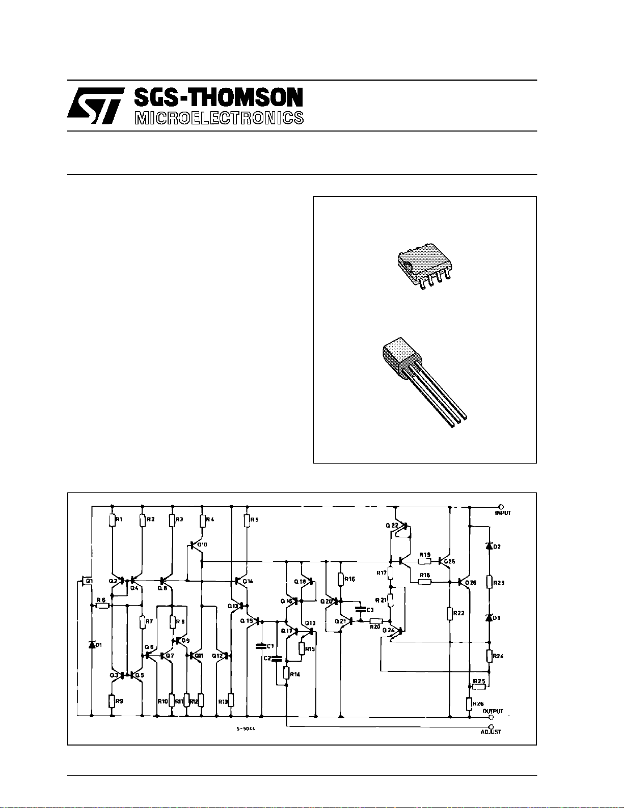
The LM217L/LM317L are monolithic integrated circuit in SO-8and TO-92packagesintended foruse
as positiveadjustable voltage regulators.
They are designed to supply until 100 mA of load
current with anoutput voltageadjustableover a 1.2
to 37V range.
The nominal output voltage is selected bymeans of
only a resistive divider, making the device exceptionally easy to use and eliminating the stockingof
many fixed regulators.
LM217L
LM317L
LOW CURRENT
SO-8
TO-92
SCHEM ATIC D IA G RA M
April1994
1/8
Page 2
LM217L/LM317L
ABSOLUTE MAXIMUM RAT ING
Symbol Parameter Value Unit
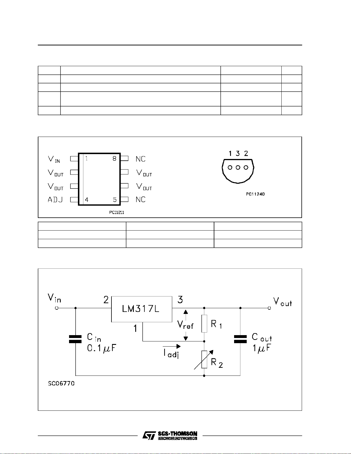
V
PIN CONNEC TION AND OR DE RI NG N U MBER
Input-Output Differential Voltage 40 V
i-Vo
Power Dissipation Internally Limited
P
d
Operating Junction Temperature Range for LM217L
T
opr
for LM317L
Storage Temperature Range -55 to 150
T
stg
-40 to 125
0 to 125
SO-8 TO-92
pin 1 = ADJUST
pin 2 = IN
pin 3 = OUT
BOTTOM VIEW
o
C
o
C
o
C
Type SO-8 TO-92
LM217L LM217LD LM217LZ
LM317L LM317LD LM317LZ
TEST CIRCUIT
2/8
Page 3
LM217L / LM 3 17L
ELECT R I CAL CHARACT ER I STICS FOR LM 217L (Refer to t he test circ ui ts, -40 ≤ Tj≤ 125oC
Vi-Vo=5V,Io= 40 mA, unless otherw is e s pecified)
Symbol Parameter Test Conditions Min. Typ. Max. Unit
∆V
Line Regulation Vi-Vo= 3 to 40 V
o
IL<20mA
∆V
Load Regulation Vo≤ 5V
o
Io= 5 mA to 100 mA
V
≥ 5V
o
Io= 5 mA to 100 mA
I
Adjustment Pin Current 50 100 µA
ADJ
∆I
Adjustment Pin Current Vi-Vo= 3 to 40 V
ADJ
Io= 5 mA to 100 mA Pd< 625 mW
V
Reference Voltage Vi-Vo= 3 to 40 V
REF
Io= 5 mA to 100 mA Pd< 625 mW
∆
V
Output Voltage Temperature
o
Stability
V
o
I
I
o(max)
Minimum Load Current Vi-Vo= 40 V 3.5 5 mA
o(min)
Maximum Output Current Vi-Vo= 3 to 13 V
Vi-Vo=40V
e
Output Noise Voltage
N
(percentance of V
)
O
SVR Supply Voltage Rejection (*) T
B = 10Hz to 10KHz
Tj=25oC
=25oC
j
f = 120 Hz
(*) CADJ is connected between Adjust pin and Ground.
Tj=25oC 0.01 0.02 %/V
0.02 0.05 %/V
Tj=25oC 5 15 mV
20 50 mV
Tj=25oC 0.1 0.3 %
0.3 1 %
0.2 5 µA
1.2 1.25 1.3 V
0.7 %
100 200
mA
50
0.003 %
C
=0 65 dB
ADJ
C
=10µF66 80 dB
ADJ
ELECT R I CAL CHARACT ER I STICS FOR LM 317L (Refer to t he test circ ui ts, 0 ≤ Tj≤ 125oC
Vi-Vo=5V,Io= 40 mA, unless otherw is e s pecified)
Symbol Parameter Test Conditions Min. Typ. Max. Unit
∆V
Line Regulation Vi-Vo= 3 to 40 V
∆I
o
∆V
Load Regulation Vo≤ 5V
o
I
Adjustment Pin Current 50 100 µA
ADJ
Adjustment Pin Current Vi-Vo= 3 to 40 V
ADJ
I
<20mA
L
I
= 5 mA to 100 mA
o
V
≥ 5V
o
I
= 5 mA to 100 mA
o
Io= 5 mA to 100 mA Pd< 625 mW
V
Reference Voltage Vi-Vo= 3 to 40 V
REF
Io= 5 mA to 100 mA Pd< 625 mW
∆
V
Output Voltage Temperature
o
Stability
V
o
I
I
o(max)
Minimum Load Current Vi-Vo= 40 V 3.5 5 mA
o(min)
Maximum Output Current Vi-Vo= 3 to 13 V
Vi-Vo=40V
e
Output Noise Voltage
N
(percentance of VO)
SVR Supply Voltage Rejection (*) T
B = 10Hz to 10KHz
Tj=25oC
=25oC
j
f = 120 Hz
(*) CADJ is connected between Adjust pin and Ground.
=25oC 0.01 0.04 %/V
T
j
0.02 0.07 %/V
=25oC 5 25 mV
T
j
20 70 mV
=25oC 0.1 0.5 %
T
j
0.3 1.5 %
0.2 5 µA
1.2 1.25 1.3 V
0.7 %
100 200
50
0.003 %
C
=0 65 dB
ADJ
C
=10µF66 80 dB
ADJ
mA
3/8
Page 4

LM217L/LM317L
Current Limit Minimum Operating Current
APPLICATION INFORMATION
The LM317Lprovides an internal reference voltage
of 1.25V between the output and adjustments terminals. This is usedto set a constant current flow
acrossanexternalresistordivider (seefig.4),giving
an output voltageVO of:
R
VO=V
REF
The devicewas designed to minimize the term I
(1 +
R
2
) +I
1
ADJR2
ADJ
(100µA max) and to maintain it very constant with
line and load changes. Usually, the error term
IADJ⋅R2 can be neglected. To obtain the previous
requirement, all the regulator quiescent current is
returned totheoutputterminal,imposing a minimum
load current condition. If theload is insufficient, the
outputvoltage will rise.
Since theLM317Lis a floating regulator and ”sees”
onlytheinput-to-output differentialvoltage, supplies
of very high voltagewith respect to ground can be
regulated as long as the maximum input-to-output
differential is not exceeded. Furthermore, programmable regulator are easily obtainable and, by connecting a fixedresistor between theadjustment and
output,thedevice canbeusedasaprecision current
regulator.
In order to optimisethe load regulation, the current
set resistor R1 (see fig. 4) should be tied as close
as possible to the regulator, while the ground terminal of R2 should be near the ground of the load
to provideremote groundsensing.
Figure 4 : Basic Adjustable Regulator.
LM 317L
4/8
Page 5

Voltage Regulator with Protection Diodes.
LM31 7L
Slow Turn-on 15V Regulator. Current Regulator.
LM217L / LM 3 17L
LM317L
LM317L
V
ref
I
=
o
+
R
1
I
ADJ
≈
1.25
R
V
1
5V Electronic Shut-down Regulator. Digitally Selected Outputs.
LM 317L
LM317L
(R2 sets maximum Vo)
5/8
Page 6

LM217L/LM317L
SO8 MECHANICAL DATA
DIM.
MIN. TYP. MAX. MIN. TYP. MAX.
A 1.75 0.068
a1 0.1 0.25 0.003 0.009
a2 1.65 0.064
a3 0.65 0.85 0.025 0.033
b 0.35 0.48 0.013 0.018
b1 0.19 0.25 0.007 0.010
C 0.25 0.5 0.010 0.019
c1 45° (typ.)
D 4.8 5.0 0.188 0.196
E 5.8 6.2 0.228 0.244
e 1.27 0.050
e3 3.81 0.150
F 3.8 4.0 0.14 0.157
L 0.4 1.27 0.015 0.050
M 0.6 0.023
S8°(max.)
mm inch
6/8
P013M
Page 7

TO-92 MECHANICAL DATA
LM217L / LM 3 17L
DIM.
mm inch
MIN. TYP. MAX. MIN. TYP. MAX.
A 4.58 5.33 0.180 0.210
B 4.45 5.2 0.175 0.204
C 3.2 4.2 0.126 0.165
D 12.7 0.500
E 1.27 0.050
F 0.4 0.51 0.016 0.020
G 0.35 0.14
EE
C
AD
B
F
G
G
7/8
Page 8

LM217L/LM317L
Information furnished is believed to be accurate and reliable. However, SGS-THOMSON Microelectronics assumes no responsability for the
consequences of use of such information nor for any infringement of patents or other rights of third parties which may results from its use. No
license is grantedby implication or otherwise under anypatent or patent rights of SGS-THOMSON Microelectronics.Specificationsmentioned
in this publicationare subject to change without notice. This publication supersedes and replaces all information previously supplied.
SGS-THOMSON Microelectronicsproductsare not authorizedforuse as criticalcomponents inlife supportdevices or systems withoutexpress
written approval of SGS-THOMSON Microelectonics.
1994SGS-THOMSON Microelectronics- All RightsReserved
Australia - Brazil - France - Germany - Hong Kong - Italy -Japan - Korea - Malaysia - Malta - Morocco - The Netherlands -
Singapore - Spain - Sweden - Switzerland -Taiwan - Thailand - UnitedKingdom - U.S.A
SGS-THOMSON Microelectronics GROUPOF COMPANIES
8/8
 Loading...