

Page 1
October 17, 2008
LM3151/LM3152/LM3153
SIMPLE SWITCHER® CONTROLLER, 42V Synchronous
Step-Down
LM3151/LM3152/LM3153 SIMPLE SWITCHER
General Description
The LM3151/2/3 SIMPLE SWITCHER® Controller is an easy
to use and simplified step down power controller capable of
providing up to 12A of output current in a typical application.
Operating with an input voltage range of 6V-42V, the
LM3151/2/3 features a fixed output voltage of 3.3V, and features switching frequencies of 250 kHz, 500 kHz, and 750
kHz. The synchronous architecture provides for highly efficient designs. The LM3151/2/3 controller employs a Constant
On-Time (COT) architecture with a proprietary Emulated Ripple Mode (ERM) control that allows for the use of low ESR
output capacitors, which reduces overall solution size and
output voltage ripple. The Constant On-Time (COT) regulation architecture allows for fast transient response and requires no loop compensation, which reduces external component count and reduces design complexity.
Fault protection features such as thermal shutdown, undervoltage lockout, over-voltage protection, short-circuit protection, current limit, and output voltage pre-bias startup allow for
a reliable and robust solution.
The LM3151/2/3 SIMPLE SWITCHER® concept provides for
an easy to use complete design using a minimum number of
external components and National’s WEBENCH® online design tool. WEBENCH® provides design support for every step
of the design process and includes features such as external
component calculation with a new MOSFET selector, electrical simulation, thermal simulation, and Build-It boards for
prototyping.
Features
PowerWise® step-down controller
■
6V to 42V Wide input voltage range
■
Fixed output voltage of 3.3V
■
Fixed switching frequencies of 250 kHz/500 kHz/750 kHz
■
No loop compensation required
■
Fully WEBENCH® enabled
■
Low external component count
■
Constant On-Time control
■
Ultra-Fast transient response
■
Stable with low ESR capacitors
■
Output voltage pre-bias startup
■
Valley current limit
■
Programmable soft-start
■
Typical Applications
Telecom
■
Networking Equipment
■
Routers
■
Security Surveillance
■
Power Modules
■
®
CONTROLLER, 42V Synchronous Step-Down
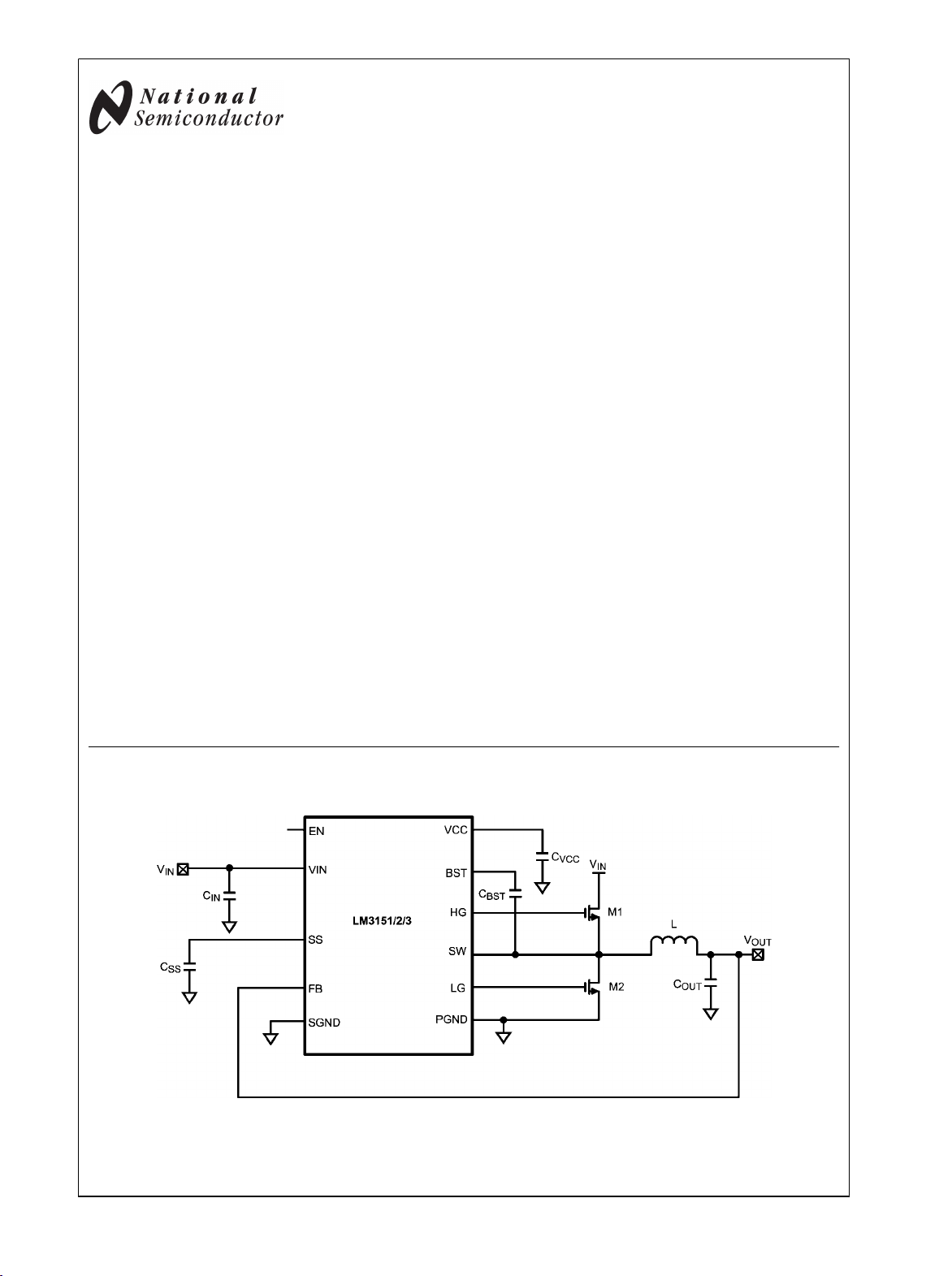
Typical Application
30053201
SIMPLE SWITCHER® is a registered trademark of National Semiconductor Corporation
© 2008 National Semiconductor Corporation 300532 www.national.com
Page 2
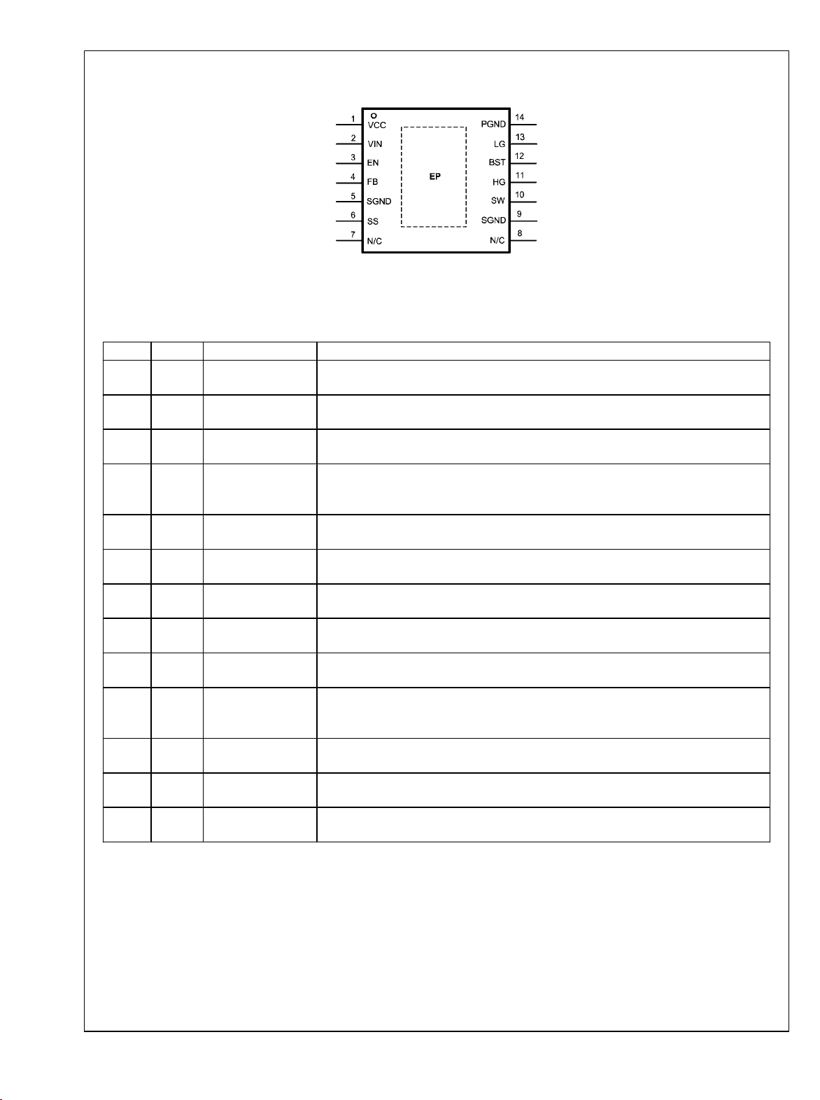
Connection Diagram
LM3151/LM3152/LM3153
Pin Descriptions
Pin Name Description Function
1 VCC
2 VIN Input Supply Voltage
3 EN Enable
4 FB Feedback
5,9 SGND Signal Ground
6 SS Soft-Start
7,8 N/C Not Connected
10 SW Switch Node
11 HG
12 BST
13 LG Low-Side Gate Drive
14 PGND Power Ground
EP EP Exposed Pad
Supply Voltage for
FET Drivers
High-Side Gate
Drive
Connection for
Bootstrap Capacitor
Nominally regulated to 5.95V. Connect a 1 µF to 2.2 µF decoupling capacitor from this
pin to ground.
Supply pin to the device. Nominal input range is 6V to 42V. See ordering information
for Vin limitations.
To enable the IC apply a logic high signal to this pin greater than 1.26V typical or leave
floating. To disable the part, ground the EN pin.
Internally connected to the resistor divider network which sets the fixed output voltage.
This pin also senses the output voltage faults such a over-voltage and short circuit
conditions.
Ground for all internal bias and reference circuitry. Should be connected to PGND at a
single point.
An internal 7.7 µA current source charges an external capacitor to provide the soft-start
function.
Internally not electrically connected. These pins may be left unconnected or connected
to ground.
Switch pin of controller and high-gate driver lower supply rail. A boost capacitor is also
connected between this pin and BST pin
Gate drive signal to the high-side NMOS switch. The high-side gate driver voltage is
supplied by the differential voltage between the BST pin and SW pin.
High-gate driver upper supply rail. Connect a 0.33 µF-0.47 µF capacitor from SW pin to
this pin. An internal diode charges the capacitor during the high-side switch off-time. Do
not connect to an external supply rail.
Gate drive signal to the low-side NMOS switch. The low-side gate driver voltage is
supplied by VCC.
Synchronous rectifier MOSFET source connection. Tie to power ground plane. Should
be tied to SGND at a single point.
Exposed die attach pad should be connected directly to SGND. Also used to help
dissipate heat out of the IC.
eTSSOP-14
30053202
www.national.com 2
Page 3
Ordering Information
LM3151/LM3152/LM3153
Order Number Package Type NSC Package
Drawing
LM3151MH-3.3
LM3151MHE-3.3 250 Units in Tape and
LM3151MHX-3.3 2500 Units in Tape and
LM3152MH-3.3
LM3152MHE-3.3 250 Units in Tape and
LM3152MHX-3.3 2500 Units in Tape and
LM3153MH-3.3
LM3153MHE-3.3 250 Units in Tape and
LM3153MHX-3.3 2500 Units in Tape and
LM3151MH-2.5
LM3151MHE-2.5
LM3151MHX-2.5
LM3152MH-2.5
LM3152MHX-2.5
LM3153MH-2.5
LM3153MHX-2.5
LM3151MH-5.0
LM3151MHX-5.0
LM3152MH-5.0
LM3152MHX-5.0
LM3153MH-5.0
LM3153MHX-5.0
eTSSOP-14 MXA14A 6V - 42V 3.3V 250KHz
eTSSOP-14 MXA14A 6V - 33V 3.3V 500KHz
eTSSOP-14 MXA14A 8V - 18V 3.3V 750KHz
eTSSOP-14 MXA14A
eTSSOP-14 MXA14A
Input
Voltage
Range
*
* 500KHzLM3152MHE-2.5
* 750KHzLM3153MHE-2.5
*
* 500KHzLM3152MHE-5.0
* 750KHzLM3153MHE-5.0
Output
Voltage
2.5V
5.0V
Switching
Frequency
250KHz
250KHzLM3151MHE-5.0
Supplied As
94 Units per Anti-Static
Tube
Reel
Reel
94 Units per Anti-Static
Tube
Reel
Reel
94 Units per Anti-Static
Tube
Reel
Reel
*Coming Soon
3 www.national.com
Page 4
Absolute Maximum Ratings (Note 1)
If Military/Aerospace specified devices are required,
please contact the National Semiconductor Sales Office/
All Other Inputs to GND -0.3V to 7V
ESD Rating (Note 2) 2kV
Storage Temperature Range -65°C to +150°C
Distributors for availability and specifications.
VIN to GND -0.3V to 47V
SW to GND -3V to 47V
BST to SW -0.3V to 7V
BST to GND -0.3V to 52V
LM3151/LM3152/LM3153
Electrical Characteristics Limits in standard type are for T
Operating Ratings (Note 1)
V
IN
Junction Temperature Range (TJ)
EN 0V to 5V
= 25°C only; limits in boldface type apply over the
J
−40°C to + 125°C
junction temperature (TJ) range of -40°C to +125°C. Minimum and Maximum limits are guaranteed through test, design, or statistical
correlation. Typical values represent the most likely parametric norm at TJ = 25°C, and are provided for reference purposes only.
Unless otherwise stated the following conditions apply: VIN = 18V.
Symbol Parameter Conditions Min Typ Max Units
Start-Up Regulator, VCC
V
CC
VIN - V
I
VCCL
VCC
UVLO
V
CC-UVLO-HYS
t
CC-UVLO-D
I
IN
I
IN-SD
CC
VIN - VCC Dropout Voltage
VCC Current Limit (Note 3) VCC = 0V 65 100
VCC Under-voltage Lockout threshold
(UVLO)
VCC UVLO Hysteresis
VCC UVLO Filter Delay
Input Operating Current No Switching
Input Operating Current, Device
Shutdown
C
= 1 µF, 0 mA to 40 mA 5.65 5.95 6.25
VCC
I
= 2 mA, Vin = 5.5V 40
VCC
I
= 30 mA, Vin = 5.5V 330
VCC
VCC Increasing
VCC Decreasing
4.75 5.1 5.40
475
3
3.6 5.2
VEN = 0V
32 55
GATE Drive
I
Q-BST
R
DS-HG-Pull-Up
R
DS-HG-Pull-Down
R
DS-LG-Pull-Up
R
DS-LG-Pull-Down
Boost Pin Leakage
HG Drive Pull–Up On-Resistance
HG Drive Pull–Down On-Resistance
LG Drive Pull–Up On-Resistance
LG Drive Pull–Down On-Resistance
V
– VSW = 6V 2
BST
IHG Source = 200 mA 5
IHG Sink = 200 mA 3.4
ILG Source = 200 mA 3.4
ILG Sink = 200 mA 2
Soft-Start
I
SS
I
SS-DIS
SS Pin Source Current
SS Pin Discharge Current
VSS = 0V 5.9 7.7 9.5
200
Current Limit
V
CL
Current Limit Voltage Threshold
175 200 225
ON/OFF Timer
t
ON-MIN
t
OFF
ON Timer Minimum Pulse Width
OFF Timer Minimum Pulse Width
200
370 525
Enable Input
V
V
EN-HYS
EN
EN Pin Input Threshold Trip Point
EN Pin threshold Hysteresis
VEN Rising 1.14 1.20 1.26
VEN Falling 120
6V to 42V
V
mV
mA
V
mV
µs
mA
µA
nA
Ω
Ω
Ω
Ω
mA
µA
mV
ns
ns
V
mV
www.national.com 4
Page 5
Symbol Parameter Conditions Min Typ Max Units
Boost Diode
I
= 2 mA 0.7
V
f
Forward Voltage
BST
I
= 30 mA 1
BST
V
V
Thermal Characteristics
T
SD
θ
JA
Thermal Shutdown Rising 165 °C
Thermal Shutdown Hysteresis Falling 15 °C
Junction to Ambient
4 Layer JEDEC Printed Circuit
Board, 9 Vias, No Air Flow
2 Layer JEDEC Printed Circuit
40
140
°C/W
Board. No Air Flow
θ
JC
Junction to Case No Air Flow
4
°C/W
3.3V Output Option
Symbol Parameter Conditions Min Typ Max Units
V
V
OUT-OV
OUT
Output Voltage
Output Voltage Over-Voltage Threshold
3.234 3.3 3.366
3.83 4.00 4.17
V
V
LM3151-3.3 42
V
IN-MAX
Maximum Input Voltage (Note 4)
VLM3152-3.3 33
LM3153-3.3 18
LM3151-3.3 6
V
IN-MIN
Minimum Input Voltage (Note 4)
VLM3152-3.3 6
LM3153-3.3 8
LM3151-3.3, RON = 115 kΩ
f
S
Switching Frequency
LM3152-3.3, RON = 51 kΩ
LM3153-3.3, RON = 32 kΩ
LM3151-3.3, RON = 115 kΩ
t
ON
On-Time
LM3152-3.3, RON = 51 kΩ
LM3153-3.3, RON = 32 kΩ
R
FB
FB Resistance to Ground
250
500
750
730
400
330
566
kHz
ns
kΩ
LM3151/LM3152/LM3153
Note 1: Absolute Maximum Ratings indicate limits beyond which damage to the device may occur. Operating Ratings indicate conditions for which the device is
intended to be functional, but does not guarantee specific performance limits. For guaranteed specifications and conditions, see the Electrical Characteristics.
Note 2: The human body model is a 100 pF capacitor discharged through a 1.5 kΩ resistor into each pin. Test Method is per JESD-22-A114.
Note 3: VCC provides self bias for the internal gate drive and control circuits. Device thermal limitations limit external loading.
Note 4: The input voltage range is dependent on minimum on-time, off-time, and therefore frequency, and is also affected by optimized MOSFET selection.
5 www.national.com
Page 6
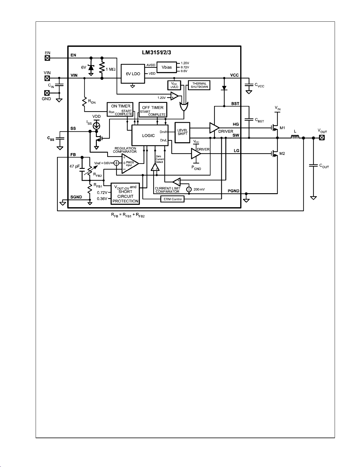
Simplified Block Diagram
LM3151/LM3152/LM3153
30053203
www.national.com 6
Page 7

Typical Performance Characteristics
LM3151/LM3152/LM3153
Boost Diode Forward Voltage vs. Temperature
30053240
Soft-Start Current vs. Temperature
Quiescent Current vs. Temperature
30053242
VCC Current Limit vs. Temperature
VCC Dropout vs. Temperature
30053243
30053248
30053247
VCC vs. Temperature
30053249
7 www.national.com
Page 8

VCL vs. Temperature
LM3151/LM3152/LM3153
On-Time vs. Temperature (250 kHz)
On-Time vs. Temperature (500 kHz)
30053282
30053284
30053283
On-Time vs. Temperature (750 kHz)
30053286
www.national.com 8
Page 9

LM3151/LM3152/LM3153
Theory of Operation
The LM3151/2/3 synchronous step-down SIMPLE SWITCHER® Controller employs a Constant On-Time (COT) architecture which is a derivative of the hysteretic control scheme.
COT relies on a fixed switch on-time to regulate the output.
The on-time of the high-side switch is set internally by resistor
RON. The LM3151/2/3 automatically adjusts the on-time inversely with the input voltage to maintain a constant frequency. Assuming an ideal system and VIN is much greater than
1V, the following approximations can be made:
The on-time, tON:
Where K = 100 pC, and RON is specified in the electrical characteristics table.
Control is based on a comparator and the on-timer, with the
output voltage feedback (FB) attenuated and then compared
with an internal reference of 0.6V. If the attenuated FB level
is below the reference, the high-side switch is turned on for a
fixed time, tON, which is determined by the input voltage and
the internal resistor, RON. Following this on-time, the switch
remains off for a minimum off-time, t
Electrical Characteristics table or until the attenuated FB voltage is less than 0.6V. This switching cycle will continue while
maintaining regulation. During continuous conduction mode
(CCM), the switching frequency depends only on duty cycle
and on-time. The duty cycle can be calculated as:
, as specified in the
OFF
1) Minimum off time as specified in the electrical characteristics table
2) The error comparator sampled voltage falls below 0.6V
Over-Voltage Comparator
The over-voltage comparator is provided to protect the output
from over-voltage conditions due to sudden input line voltage
changes or output loading changes. The over-voltage comparator continuously monitors the attenuated FB voltage versus a 0.72V internal reference. If the voltage at FB rises above
0.72V the on-time pulse is immediately terminated. This condition can occur if the input or the output load changes suddenly. Once the over-voltage protection is activated, the HG
and LG signals remain off until the attenuated FB voltage falls
below 0.72V.
Current Limit
Current limit detection occurs during the off-time by monitoring the current through the low-side switch. If during the offtime the current in the low-side switch exceeds the user
defined current limit value, the next on-time cycle is immediately terminated. Current sensing is achieved by comparing
the voltage across the low-side switch against an internal reference value, VCL, of 200 mV. If the voltage across the lowside switch exceeds 200 mV, the current limit comparator will
trigger logic to terminate the next on-time cycle. The current
limit ICL, can be determined as follows:
Where the switching frequency of a COT regulator is:
Typical COT hysteretic controllers need a significant amount
of output capacitor ESR to maintain a minimum amount of
ripple at the FB pin in order to switch properly and maintain
efficient regulation. The LM3151/2/3 however utilizes proprietary, Emulated Ripple Mode Control Scheme (ERM) that
allows the use of ceramic output capacitors without additional
equivalent series resistance (ESR) compensation. Not only
does this reduce the need for output capacitor ESR, but also
significantly reduces the amount of output voltage ripple seen
in a typical hysteretic control scheme. The output ripple voltage can become so low that it is comparable to voltage-mode
and current-mode control schemes.
Regulation Comparator
The output voltage is sampled through the FB pin and then
divided down by two internal resistors and compared to the
internal reference voltage of 0.6V by the error comparator. In
normal operation, an on-time period is initiated when the sampled output voltage at the input of the error comparator falls
below 0.6V. The high-side switch stays on for the specified
on-time, causing the sampled voltage on the error comparator
input to rise above 0.6V. After the on-time period, the highside switch stays off for the greater of the following:
Where I
value, R
at the expected maximum FET junction temperature, VCL is
the internal current limit reference voltage and Tj is the junction temperature of the LM3151/2/3.
Figure 1 illustrates the inductor current waveform. During normal operation, the output current ripple is dictated by the
switching of the FETs. The current through the low-side
switch, I
and compared to the current limit threshold voltage, VCL. The
valley current can be calculated as follows:
Where I
to-peak inductor ripple current.
If an overload condition occurs, the current through the lowside switch will increase which will cause the current limit
comparator to trigger the logic to skip the next on-time cycle.
The IC will then try to recover by checking the valley current
during each off-time. If the valley current is greater than or
equal to ICL, then the IC will keep the low-side FET on and
allow the inductor current to further decay.
Throughout the whole process, regardless of the load current,
the on-time of the controller will stay constant and thereby the
positive ripple current slope will remain constant. During each
on-time the current ramps up an amount equal to:
is the user-defined average output current limit
OCL
DS(ON)max
valley
OUT
is the resistance value of the low-side FET
, is sampled at the end of each switching cycle
is the average output current and ΔIL is the peak-
9 www.national.com
Page 10

The valley current limit feature prevents current runaway conditions due to propagation delays or inductor saturation since
LM3151/LM3152/LM3153
FIGURE 1. Inductor Current - Current Limit Operation
the inductor current is forced to decay following any overload
conditions.
30053212
Short-Circuit Protection
The LM3151/2/3 will sense a short-circuit on the output by
monitoring the output voltage. When the attenuated feedback
voltage has fallen below 60% of the reference voltage, V
0.6 (≈ 0.36V), short-circuit mode of operation will start. During
ref
short-circuit operation, the SS pin is discharged and the output voltage will fall to 0V. The SS pin voltage, VSS, is then
ramped back up at the rate determined by the SS capacitor
and ISS until VSS reaches 0.7V. During this re-ramp phase, if
the short-circuit fault is still present the output current will be
equal to the set current limit. Once the soft-start voltage
reaches 0.7V the output voltage is sensed again and if the
attenuated VFB is still below V
charged again and the cycle repeats until the short-circuit fault
x 0.6 then the SS pin is dis-
ref
is removed.
Soft-Start
The soft-start (SS) feature allows the regulator to gradually
reach a steady-state operating point, which reduces start-up
stresses and current surges. At turn-on, while VCC is below
the under-voltage threshold, the SS pin is internally grounded
and V
ramp VFB from 0V to it's final output voltage as programmed
by the internal resistor divider. By changing the soft-start capacitor value, the duration of start-up can be changed accordingly. The start-up time can be calculated using the
following equation:
Where tSS is measured in seconds, V
soft-start pin source current, which is typically 7.7 µA (refer to
electrical characteristics table).
is held at 0V. The SS capacitor is used to slowly
OUT
= 0.6V and ISS is the
ref
An internal switch grounds the SS pin if VCC is below the
under-voltage lockout threshold, if a thermal shutdown occurs, or if the EN pin is grounded. By using an externally
controlled switch, the output voltage can be shut off by
x
grounding the SS pin.
During startup the LM3151/2/3 will operate in diode emulation
mode, where the low-side gate LG will turn off and remain off
when the inductor current falls to zero. Diode emulation mode
allows for start up into a pre-biased output voltage. When softstart is greater than 0.7V, the LM3151/2/3 will remain in
continuous conduction mode. During diode emulation mode
at current limit the low-gate will remain off when the inductor
current is off.
The soft start time should be greater than the rise time specified by,
tSS ≥ (V
OUT
x C
OUT
) / (I
OCL
- I
OUT
)
Enable/Shutdown
The EN pin can be activated by either leaving the pin floating
due to an internal pull up resistor to VIN or by applying a logic
high signal to the EN pin of 1.26V or greater. The LM3151/2/3
can be remotely shut down by taking the EN pin below 1.02V.
Low quiescent shutdown is achieved when VEN is less than
0.4V. During low quiescent shutdown the internal bias circuitry is turned off.
The LM3151/2/3 has certain fault conditions that can trigger
shutdown, such as over-voltage protection, current limit, under-voltage lockout, or thermal shutdown. During shutdown,
the soft-start capacitor is discharged. Once the fault condition
is removed, the soft-start capacitor begins charging, allowing
the part to start up in a controlled fashion. In conditions where
there may be an open drain connection to the EN pin, it may
be necessary to add a 1000 pF bypass capacitor to this pin.
This will help decouple noise from the EN pin and prevent
false disabling.
www.national.com 10
Page 11

LM3151/LM3152/LM3153
Thermal Protection
The LM3151/2/3 should be operated such that the junction
temperature does not exceed the maximum operating junction temperature. An internal thermal shutdown circuit, which
activates at 165°C (typical), takes the controller to a low-power reset state by disabling the buck switch and the on-timer,
and grounding the SS pin. This feature helps prevent catastrophic failures from accidental device overheating. When the
junction temperature falls back below 150°C the SS pin is released and normal operation resumes.
Design Guide
The design guide provides the equations required to design
with the LM3151/2/3 SIMPLE SWITCHER® Controller.
WEBENCH® design tool can be used with or in place of this
section for a more complete and simplified design process.
1. Define Power Supply Operating Conditions
a. Maximum and Minimum DC Input voltage
b. Maximum Expected Load Current during normal operation
c. Target Switching Frequency
2. Determine which IC Controller to Use
The desired input voltage range will determine which version
of the LM3151/2/3 controller will be chosen. The higher
switching frequency options allow for physically smaller inductors but efficiency may decrease.
3. Determine Inductor Required Using Figure 2
To use the nomograph below calculate the inductor volt-microsecond constant ET from the following formula:
Where fS is in kHz units. The intersection of the Load Current
and the Volt-microseconds lines on the chart below will determine which inductors are capable for use in the design. The
chart shows a sample of parts that can be used. The offline
calculator tools and WEBENCH® will fully calculate the requirements for the components needed for the design.
FIGURE 2. Inductor Nomograph
11 www.national.com
30053252
Page 12

TABLE 1. Inductor Selection Table
Inductor Designator Inductance (µH) Current (A) Part Name Vendor
L01 47 7-9
L02 33 7-9 SER2817H-333KL COILCRAFT
L03 22 7-9 SER2814H-223KL COILCRAFT
L04 15 7-9 7447709150 WURTH
L05 10 7-9 RLF12560T-100M7R5 TDK
LM3151/LM3152/LM3153
L06 6.8 7-9 B82477-G4682-M EPCOS
L07 4.7 7-9 B82477-G4472-M EPCOS
L08 3.3 7-9 DR1050-3R3-R COOPER
L09 2.2 7-9 MSS1048-222 COILCRAFT
L10 1.5 7-9 SRU1048-1R5Y BOURNS
L11 1 7-9 DO3316P-102 COILCRAFT
L12 0.68 7-9 DO3316H-681 COILCRAFT
L13 33 9-12
L14 22 9-12 SER2918H-223 COILCRAFT
L15 15 9-12 SER2814H-153KL COILCRAFT
L16 10 9-12 7447709100 WURTH
L17 6.8 9-12 SPT50H-652 COILCRAFT
L18 4.7 9-12 SER1360-472 COILCRAFT
L19 3.3 9-12 MSS1260-332 COILCRAFT
L20 2.2 9-12 DR1050-2R2-R COOPER
L21 1.5 9-12 DR1050-1R5-R COOPER
L22 1 9-12 DO3316H-102 COILCRAFT
L23 0.68 9-12
L24 0.47 9-12
L25 22 12-15 SER2817H-223KL COILCRAFT
L26 15 12-15
L27 10 12-15 SER2814L-103KL COILCRAFT
L28 6.8 12-15 7447709006 WURTH
L29 4.7 12-15 7447709004 WURTH
L30 3.3 12-15
L31 2.2 12-15
L32 1.5 12-15 MLC1245-152 COILCRAFT
L33 1 12-15
L34 0.68 12-15 DO3316H-681 COILCRAFT
L35 0.47 12-15
L36 0.33 12-15 DR73-R33-R COOPER
L37 22 15-
L38 15 15- SER2817H-153KL COILCRAFT
L39 10 15- SER2814H-103KL COILCRAFT
L40 6.8 15-
L41 4.7 15- SER2013-472ML COILCRAFT
L42 3.3 15- SER2013-362L COILCRAFT
L43 2.2 15-
L44 1.5 15- HA3778-AL COILCRAFT
L45 1 15- B82477-G4102-M EPCOS
L46 0.68 15-
L47 0.47 15-
L48 0.33 15-
www.national.com 12
Page 13

4. Determine Output Capacitance
Typical hysteretic COT converters similar to the LM3151/2/3
require a certain amount of ripple that is generated across the
ESR of the output capacitor and fed back to the error comparator. Emulated Ripple Mode control built into the
LM3151/2/3 will recreate a similar ripple signal and thus the
requirement for output capacitor ESR will decrease compared
to a typical Hysteretic COT converter. The emulated ripple is
generated by sensing the voltage signal across the low-side
FET and is then compared to the FB voltage at the error comparator input to determine when to initiate the next on-time
period.
2
C
Omin
= 70 / (f
s
x L)
The maximum ESR allowed to prevent over-voltage protection during normal operation is:
ESR
= (80 mV x L) / ET
ET
is calculated using V
min
max
IN-MIN
min
The minimum ESR must meet both of the following criteria:
ESR
≥ (15 mV x L) / ET
ESR
ET
is calculated using V
max
min
min
≥ [ET
/ (VIN - V
max
IN-MAX
.
OUT
max
)]/ C
O
Any additional parallel capacitors should be chosen so that
their effective impedance will not negatively attenuate the
output ripple voltage.
5. MOSFET Selection
The high-side and low-side FETs must have a drain to source
(VDS) rating of at least 1.2 x VIN.
The gate drive current from VCC must not exceed the minimum current limit of VCC. The drive current from VCC can be
calculated with:
I
VCCdrive
Where, Q
side and low-side FETs.
is the combined total gate charge of the high-
gtotal
= Q
gtotal
x f
S
Use the following equations to calculate the current limit, ICL,
as shown in Figure 1.
Tj is the junction temperature of the LM3151/2/3.
The plateau voltage of the FET VGS vs Qg curve, as shown in
Figure 3 must be less than VCC - 750 mV.
30053281
FIGURE 3. Typical MOSFET Gate Charge Curve
See following design example for estimated power dissipation
calculation.
6. Calculate Input Capacitance
The main parameters for the input capacitor are the voltage
rating, which must be greater than or equal to the maximum
DC input voltage of the power supply, and its rms current rating. The maximum rms current is approximately 50% of the
maximum load current.
Where, ΔV
age. A good starting point for the input ripple voltage is 5% of
is the maximum allowable input ripple volt-
IN-MAX
VIN.
When using low ESR ceramic capacitors on the input of the
LM3151/2/3 a resonant circuit can be formed with the
impedance of the input power supply and parasitic impedance
of long leads/PCB traces to the LM3151/2/3 input capacitors.
It is recommended to use a damping capacitor under these
circumstances, such as aluminum electrolytic that will prevent
ringing on the input. The damping capacitor should be chosen
to be approximately 5 times greater than the parallel ceramic
capacitors combination. The total input capacitance should
be greater than 10 times the input inductance of the power
supply leads/pcb trace. The damping capacitor should also
be chosen to handle its share of the rms input current which
is shared proportionately with the parallel impedance of the
ceramic capacitors and aluminum electrolytic at the
LM3151/2/3 switching frequency.
The C
The recommended value is 0.1 µF.
capacitor should be placed directly at the VIN pin.
BYP
7. Calculate Soft-Start Capacitor
LM3151/LM3152/LM3153
Where tSS is the soft-start time in seconds and V
13 www.national.com
= 0.6V.
ref
Page 14

8. C
, and C
VCC
C
should be placed directly at the VCC pin with a recom-
VCC
mended value of 1 µF to 2.2 µF. For input voltage ranges that
BST
and C
EN
include voltages below 8V a 1 µF capacitor must be used for
C
. C
VCC
creates a voltage used to drive the gate of the
BST
Design Example
LM3151/LM3152/LM3153
high-side FET. It is charged during the SW off-time. The recommended value for C
itor, CEN, recommended value is 1000 pF when driving the EN
is 0.47 µF. The EN bypass capac-
BST
pin from open drain type of signal.
30053261
FIGURE 4. Design Example Schematic
1. Define Power Supply Operating Conditions
a. V
= 3.3V
OUT
b. V
IN-MIN
= 6V, V
IN-TYP
= 12V, V
IN-MAX
= 24V
c. Typical Load Current = 12A, Max Load Current = 15A
d. Soft-Start time tSS = 5 ms
2. Determine which IC Controller to Use
The LM3151 and LM3152 allow for the full input voltage
range. However, from buck converter basic theory, the higher
switching frequency will allow for a smaller inductor. Therefore, the LM3152-3.3 500 kHz part is chosen so that a smaller
inductor can be used.
3. Determine Inductor Required
a. ET = (24-3.3) x (3.3/24) x (1000/500) = 5.7 V µs
b. From the inductor nomograph a 12A load and 5.7 V µs calculation corresponds to a L44 type of inductor.
c. Using the inductor designator L44 in Table 1 the Coilcraft
HA3778-AL 1.65 µH inductor is chosen.
4. Determine Output Capacitance
The voltage rating on the output capacitor should be greater
than or equal to the output voltage. As a rule of thumb most
capacitor manufacturers suggests not to exceed 90% of the
capacitor rated voltage. In the case of multilayer ceramics the
capacitance will tend to decrease dramatically as the applied
voltage is increased towards the capacitor rated voltage. The
capacitance can decrease by as much as 50% when the applied voltage is only 30% of the rated voltage. The chosen
capacitor should also be able to handle the rms current which
is equal to:
For this design the chosen ripple current ratio, r = 0.3, represents the ratio of inductor peak-to-peak current to load current
Iout. A good starting point for ripple ratio is 0.3 but it is acceptable to choose r between 0.25 to 0.5. The nomographs
in this datasheet all use 0.3 as the ripple current ratio.
I
= 1A
rmsco
tON = (3.3V/12V) / 500 kHz = 550 ns
Minimum output capacitance is:
2
C
= 70 / (f
Omin
C
= 70 / (500 kHz2 x 1.65 µH) = 169 µF
Omin
S
x L)
The maximum ESR allowed to prevent over-voltage protection during normal operation is:
ESR
= (80 mV x L) / ET
max
ESR
= (80 mV x 1.65 µH) / 5.7 V µs
max
ESR
= 23 mΩ
max
The minimum ESR must meet both of the following criteria:
ESR
≥ (15 mV x L) / ET
min
www.national.com 14
Page 15

LM3151/LM3152/LM3153
ESR
≥ [ET / (VIN - V
min
ESR
≥ (15 mV x 1.65 µH) / 5.7 V µs = 4.3 mΩ
min
ESR
≥ [5.7 V µs / (12 - 3.3)] / 169 µF = 3.9 mΩ
min
OUT
)] / C
O
Based on the above criteria two 150 µF polymer aluminum
capacitors with a ESR = 12 mΩ each for a effective ESR in
parallel of 6 mΩ was chosen from Panasonic. The part number is EEF-UE0J151P.
5. MOSFET Selection
The LM3151/2/3 are designed to drive N-channel MOSFETs.
For a maximum input voltage of 24V we should choose Nchannel MOSFETs with a maximum drain-source voltage,
VDS, greater than 1.2 x 24V = 28.8V. FETs with maximum
VDS of 30V will be the first option. The combined total gate
charge Q
the following:
Where I
temperature range, specified in the electrical characteristics
of the high-side and low-side FET should satisfy
gtotal
Q
≤ I
gtotal
Q
≤ 65 mA / 500 kHz
gtotal
Q
gtotal
is the minimum current limit of VCC, over the
VCCL
/ f
VCCL
≤ 130 nC
s
table. The MOSFET gate charge Qg is gathered from reading
the VGS vs Qg curve of the MOSFET datasheet at the VGS =
5V for the high-side, M1, MOSFET and VGS = 6V for the lowside, M2, MOSFET.
The Renesas MOSFET RJK0305DPB has a gate charge of
10 nC at VGS = 5V, and 12 nC at VGS = 6V. This combined
gate charge for a high-side, M1, and low-side, M2, MOSFET
12 nC + 10 nC = 22 nC is less than 130 nC calculated
Q
.
gtotal
The calculated MOSFET power dissipation must be less than
the max allowed power dissipation, Pdmax, as specified in the
MOSFET datasheet. An approximate calculation of the FET
power dissipated Pd, of the high-side and low-side FET is
given by:
High-Side MOSFET
tion temperature rise above ambient temperature and θJA =
30°C/W, can be estimated by:
Pdmax = 125°C / 30°C/W = 4.1W
The system calculated Pdh of 0.674W is much less than the
FET Pdmax of 4.1W and therefore the RJK0305DPB max allowable power dissipation criteria is met.
Low-Side MOSFET
Primary loss is conduction loss given by:
Pdl = Iout2 x R
x (1-D) = 122 x 0.01 x (1-0.275) = 1W
DS(ON)
Pdl is also less than the Pdmax specified on the RJK0305DPB
MOSFET datasheet.
However, it is not always necessary to use the same MOSFET for both the high-side and low-side. For most applications
it is necessary to choose the high-side MOSFET with the lowest gate charge and the low-side MOSFET is chosen for the
lowest allowed R
vs Qg curve must be less than VCC - 750 mV.
The current limit, I
of the low-side FET at the maximum junction temperature
(ON)
of 100°C. Then the following calculation of I
. The plateau voltage of the FET V
DS(ON)
, is calculated by estimating the R
OCL
OCL
I
= ICL + ΔIL / 2
OCL
GS
DS
is:
ICL = 200 mV / 0.014 = 14.2A
I
= 14.2A + 3.6 / 2 = 16A
OCL
6. Calculate Input Capacitance
The input capacitor should be chosen so that the voltage rating is greater than the maximum input voltage which for this
example is 24V. Similar to the output capacitor, the voltage
rating needed will depend on the type of capacitor chosen.
The input capacitor should also be able to handle the input
rms current which is approximately 0.5 x I
ple the rms input current is approximately 0.5 x 12A = 6A.
. For this exam-
OUT
The minimum capacitance with a maximum 5% input ripple
ΔV
= (0.05 x 12) = 0.6V:
IN-MAX
CIN = [12 x 0.275 x (1-0.275)] / [500 kHz x 0.6] = 8 µF
To handle the large input rms current 2 ceramic capacitors
are chosen at 10 µF each with a voltage rating of 50V and
case size of 1210, that can handle 3A of rms current each. A
100 µF aluminum electrolytic is chosen to help dampen input
ringing.
C
= 0.1 µF ceramic with a voltage rating greater than max-
BYP
imum V
IN
7. Calculate Soft-Start Capacitor
The soft start-time should be greater than the input voltage
rise time and also satisfy the following equality to maintain a
smooth transition of the output voltage to the programmed
regulation voltage during startup.
The max power dissipation of the RJK0305DPB is rated as
45W for a junction temperature that is 125°C higher than the
case temperature and a thermal resistance from the FET
junction to case, θJC, of 2.78°C/W. When the FET is mounted
onto the PCB, the PCB will have some additional thermal resistance such that the total system thermal resistance of the
FET package and the PCB, θJA, is typically in the range of 30°
C/W for this type of FET package. The max power dissipation,
Pdmax, with the FET mounted onto a PCB with a 125°C junc-
tSS ≥ (V
OUT
x C
OUT
) / (I
OCL
- I
OUT
)
5 ms > (3.3V x 300 µF) / (1.2 x 12A - 12A)
5 ms > 0.412 ms
The desired soft-start time, tSS, of 5 ms satisfies the equality
as shown above. Therefore, the soft-start capacitor, CSS, is
calculated as:
CSS = (7.7 µA x 5 ms) / 0.6V = 0.064 µF
15 www.national.com
Page 16

Let CSS = 0.068 µF, which is the next closest standard value.
This should be a ceramic cap with a voltage rating greater
than 10V.
Bill of Materials
Designator Value Parameters Manufacturer Part Number
C
C
C
IN2
OUT1
BST
C
BYP
C
EN
C
IN1
, C
IN3
, C
OUT2
C
SS
C
VCC
LM3151/LM3152/LM3153
L1 1.65 µH
M1, M2 30V
U1 National Semiconductor LM3152MH-3.3
0.47 µF Ceramic, X7R, 16V, 10% TDK C2012X7R1C474K
0.1 µF Ceramic, X7R, 50V, 10% TDK C2012X7R1H104K
1000 pF Ceramic, X7R, 50V, 10% TDK C1608X7R1H102K
100 µF AL, EEV-FK, 63V, 20% Panasonic EEV-FK1J101P
10 µF Ceramic, X5R, 35V, 10% Taiyo Yuden GMK325BJ106KN-T
150 µF AL, UE, 6.3V, 20% Panasonic EEF-UE0J151R
0.068 µF Ceramic, 16V, 10% 0603YC683KAT2A
1 µF Ceramic, X7R, 16V, 10% Kemet C0805C105K4RACTU
Shielded Drum Core, A, 2.53 mΩ
8 nC, R
@4.5V = 10 mΩ
DS(ON)
8. C
, CEN, and C
VCC
C
= 1µF ceramic with a voltage rating greater than 10V
VCC
BST
CEN = 1000 pF ceramic with a voltage rating greater than 10V
C
= 0.47 µF ceramic with a voltage rating greater than 10V
BST
Coilcraft Inc. HA3778-AL
Renesas RJK0305DB
www.national.com 16
Page 17

PCB Layout Considerations
It is good practice to layout the power components first, such
as the input and output capacitors, FETs, and inductor. The
first priority is to make the loop between the input capacitors
and the source of the low side FET to be very small and tie
the grounds of each directly to each other and then to the
ground plane through vias. As shown in the figure below,
when the input cap ground is tied directly to the source of the
low side FET, parasitic inductance in the power path, along
with noise coupled into the ground plane, are reduced.
The switch node is the next item of importance. The switch
node should be made only as large as required to handle the
load current. There are fast voltage transitions occurring in
the switch node at a high frequency, and if the switch node is
made too large it may act as an antennae and couple switching noise into other parts of the circuit. For high power designs
it is recommended to use a multi-layer board. The FET’s are
going to be the largest heat generating devices in the design,
and as such, care should be taken to remove the heat. On
multi layer boards using exposed-pad packages for the FET’s
such as the power-pak SO-8, vias should be used under the
FETs to the same plane on the interior layers to help dissipate
the heat and cool the FETs. For the typical single FET PowerPak type FETs the high-side FET DAP is Vin. The Vin plane
should be copied to the other interior layers to the bottom layer
for maximum heat dissipation. Likewise, the DAP of the lowside FET is connected to the SW node and it’s shape should
be duplicated to the interior layers down to the bottom layer
for maximum heat dissipation.
See the Evaluation Board application note AN-1900 for an
example of a typical multilayer board layout, and the Demonstration Board Reference Design App Note for a typical 2 layer
board layout. Each design allows for single sided component
mounting.
LM3151/LM3152/LM3153
30053258
FIGURE 5. Schematic of Parasitics
30053280
FIGURE 6. PCB Placement of Power Stage
17 www.national.com
Page 18

Physical Dimensions inches (millimeters) unless otherwise noted
LM3151/LM3152/LM3153
14-Lead eTSSOP Package
NS Package Number MXA14A
www.national.com 18
Page 19

Notes
LM3151/LM3152/LM3153
19 www.national.com
Page 20

Notes
For more National Semiconductor product information and proven design tools, visit the following Web sites at:
Products Design Support
Amplifiers www.national.com/amplifiers WEBENCH www.national.com/webench
Audio www.national.com/audio Analog University www.national.com/AU
Clock Conditioners www.national.com/timing App Notes www.national.com/appnotes
Data Converters www.national.com/adc Distributors www.national.com/contacts
Displays www.national.com/displays Green Compliance www.national.com/quality/green
Ethernet www.national.com/ethernet Packaging www.national.com/packaging
Interface www.national.com/interface Quality and Reliability www.national.com/quality
LVDS www.national.com/lvds Reference Designs www.national.com/refdesigns
Power Management www.national.com/power Feedback www.national.com/feedback
Switching Regulators www.national.com/switchers
LDOs www.national.com/ldo
LED Lighting www.national.com/led
PowerWise www.national.com/powerwise
Serial Digital Interface (SDI) www.national.com/sdi
Temperature Sensors www.national.com/tempsensors
Wireless (PLL/VCO) www.national.com/wireless
CONTROLLER, 42V Synchronous Step-Down
®
THE CONTENTS OF THIS DOCUMENT ARE PROVIDED IN CONNECTION WITH NATIONAL SEMICONDUCTOR CORPORATION
(“NATIONAL”) PRODUCTS. NATIONAL MAKES NO REPRESENTATIONS OR WARRANTIES WITH RESPECT TO THE ACCURACY
OR COMPLETENESS OF THE CONTENTS OF THIS PUBLICATION AND RESERVES THE RIGHT TO MAKE CHANGES TO
SPECIFICATIONS AND PRODUCT DESCRIPTIONS AT ANY TIME WITHOUT NOTICE. NO LICENSE, WHETHER EXPRESS,
IMPLIED, ARISING BY ESTOPPEL OR OTHERWISE, TO ANY INTELLECTUAL PROPERTY RIGHTS IS GRANTED BY THIS
DOCUMENT.
TESTING AND OTHER QUALITY CONTROLS ARE USED TO THE EXTENT NATIONAL DEEMS NECESSARY TO SUPPORT
NATIONAL’S PRODUCT WARRANTY. EXCEPT WHERE MANDATED BY GOVERNMENT REQUIREMENTS, TESTING OF ALL
PARAMETERS OF EACH PRODUCT IS NOT NECESSARILY PERFORMED. NATIONAL ASSUMES NO LIABILITY FOR
APPLICATIONS ASSISTANCE OR BUYER PRODUCT DESIGN. BUYERS ARE RESPONSIBLE FOR THEIR PRODUCTS AND
APPLICATIONS USING NATIONAL COMPONENTS. PRIOR TO USING OR DISTRIBUTING ANY PRODUCTS THAT INCLUDE
NATIONAL COMPONENTS, BUYERS SHOULD PROVIDE ADEQUATE DESIGN, TESTING AND OPERATING SAFEGUARDS.
EXCEPT AS PROVIDED IN NATIONAL’S TERMS AND CONDITIONS OF SALE FOR SUCH PRODUCTS, NATIONAL ASSUMES NO
LIABILITY WHATSOEVER, AND NATIONAL DISCLAIMS ANY EXPRESS OR IMPLIED WARRANTY RELATING TO THE SALE
AND/OR USE OF NATIONAL PRODUCTS INCLUDING LIABILITY OR WARRANTIES RELATING TO FITNESS FOR A PARTICULAR
PURPOSE, MERCHANTABILITY, OR INFRINGEMENT OF ANY PATENT, COPYRIGHT OR OTHER INTELLECTUAL PROPERTY
RIGHT.
LIFE SUPPORT POLICY
NATIONAL’S PRODUCTS ARE NOT AUTHORIZED FOR USE AS CRITICAL COMPONENTS IN LIFE SUPPORT DEVICES OR
SYSTEMS WITHOUT THE EXPRESS PRIOR WRITTEN APPROVAL OF THE CHIEF EXECUTIVE OFFICER AND GENERAL
COUNSEL OF NATIONAL SEMICONDUCTOR CORPORATION. As used herein:
Life support devices or systems are devices which (a) are intended for surgical implant into the body, or (b) support or sustain life and
whose failure to perform when properly used in accordance with instructions for use provided in the labeling can be reasonably expected
to result in a significant injury to the user. A critical component is any component in a life support device or system whose failure to perform
can be reasonably expected to cause the failure of the life support device or system or to affect its safety or effectiveness.
National Semiconductor and the National Semiconductor logo are registered trademarks of National Semiconductor Corporation. All other
brand or product names may be trademarks or registered trademarks of their respective holders.
Copyright© 2008 National Semiconductor Corporation
For the most current product information visit us at www.national.com
National Semiconductor
LM3151/LM3152/LM3153 SIMPLE SWITCHER
www.national.com
Americas Technical
Support Center
Email: support@nsc.com
Tel: 1-800-272-9959
National Semiconductor Europe
Technical Support Center
Email: europe.support@nsc.com
German Tel: +49 (0) 180 5010 771
English Tel: +44 (0) 870 850 4288
National Semiconductor Asia
Pacific Technical Support Center
Email: ap.support@nsc.com
National Semiconductor Japan
Technical Support Center
Email: jpn.feedback@nsc.com
 Loading...