

Page 1
LM113/LM313 Reference Diode
LM113/LM313 Reference Diode
December 1994
General Description
The LM113/LM313 are temperature compensated, low voltage reference diodes. They feature extremely-tight regulation over a wide range of operating currents in addition to an
unusually-low breakdown voltage and good temperature
stability.
The diodes are synthesized using transistors and resistors
in a monolithic integrated circuit. As such, they have the
same low noise and long term stability as modern IC op
amps. Further, output voltage of the reference depends only
on highly-predictable properties of components in the IC; so
they can be manufactured and supplied to tight tolerances.
Features
Y
Low breakdown voltage: 1.220V
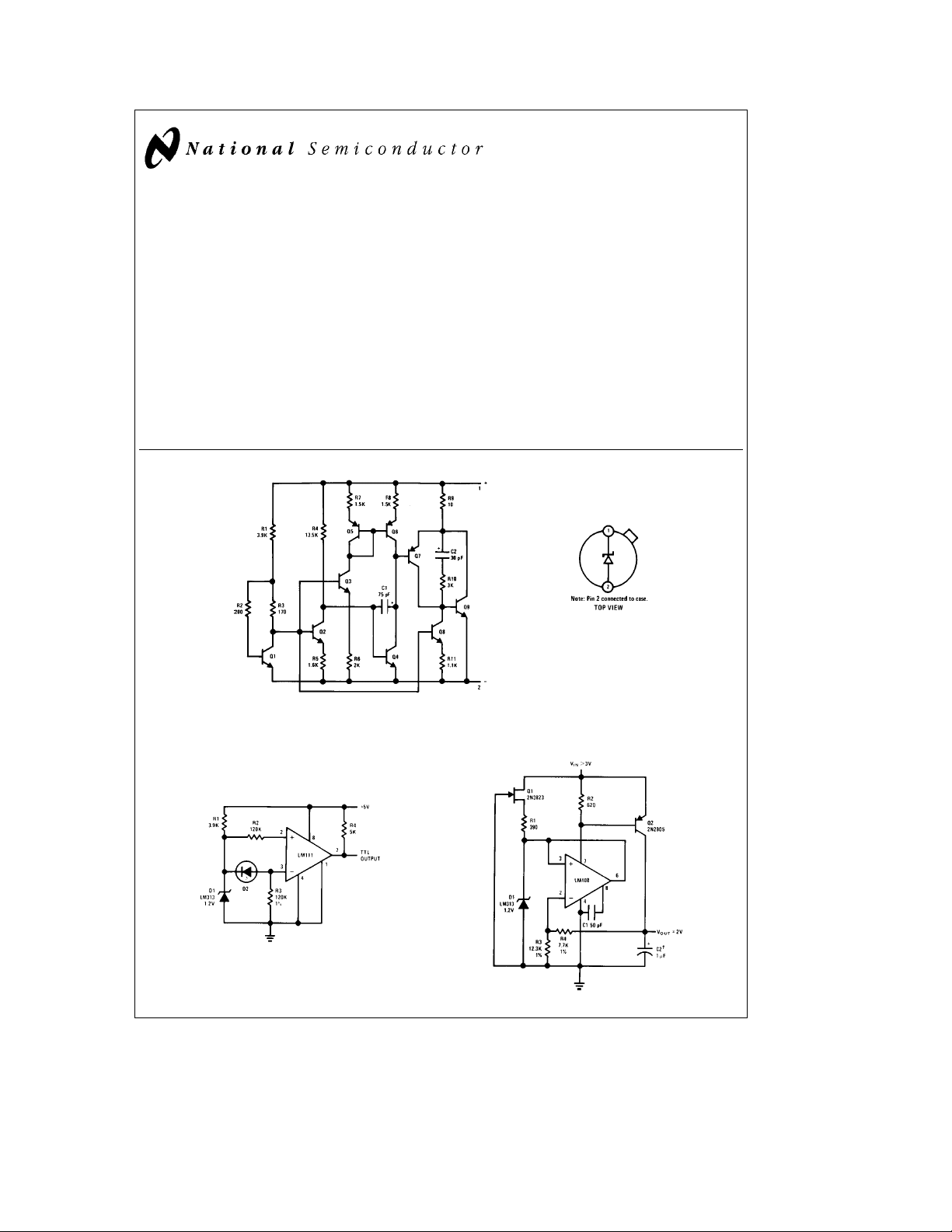
Schematic and Connection Diagrams
Y
Dynamic impedance of 0.3X from 500 mAto20mA
Y
Temperature stability typically 1% overb55§Cto125§C
range (LM113), 0
Y
Tight tolerance:g5%,g2% org1%
The characteristics of this reference recommend it for use in
bias-regulation circuitry, in low-voltage power supplies or in
battery powered equipment. The fact that the breakdown
voltage is equal to a physical property of siliconÐthe energy-band gap voltageÐmakes it useful for many temperature-compensation and temperature-measurement functions.
Cto70§C (LM313)
§
Metal Can Package
Order Number
LM113H, LM113H/883,
LM113-1H, LM113-1H/883,
LM113-2H, LM113-2H/883,
See NS Package Number H02A
or LM313H
TL/H/5713– 1
Typical Applications
Low Voltage Regulator
Level Detector for Photodiode
²
Solid tantalum.
TL/H/5713– 2
C
1995 National Semiconductor Corporation RRD-B30M115/Printed in U. S. A.
TL/H/5713
Page 2
Absolute Maximum Ratings
If Military/Aerospace specified devices are required,
please contact the National Semiconductor Sales
Office/Distributors for availability and specifications.
(Note 3)
Power Dissipation (Note 1) 100 mW
Reverse Current 50 mA
Forward Current 50 mA
Storage Temperature Range
Lead Temperature
(Soldering, 10 seconds) 300
Operating Temperature Range
LM113
LM313 0
b
65§Ctoa150§C
b
55§Ctoa125§C
Ctoa70§C
§
Electrical Characteristics (Note 2)
Parameter Conditions Min Typ Max Units
Reverse Breakdown Voltage
LM113/LM313
LM113-1 1.210 1.22 1.232 V
e
I
1mA
R
LM113-2 1.195 1.22 1.245 V
Reverse Breakdown Voltage
Change
Reverse Dynamic Impedance
Forward Voltage Drop I
RMS Noise Voltage
0.5 mA
e
I
R
e
I
R
e
F
10 Hz
e
I
R
Reverse Breakdown Voltage 0.5 mAsI
Change with Current T
MIN
Breakdown Voltage Temperature 1.0 mAsI
Coefficient T
Note 1: For operating at elevated temperatures, the device must be derated based on a 150§C maximum junction and a thermal resistance of 80
case or 440
Note 2: These specifications apply for T
inch. Kelvin contact sockets are also recommended. The diode should not be operated with shunt capacitances between 200 pF and 0.1 mF, unless isolated by at
least a 100X resistor, as it may oscillate at some currents.
Note 3: Refer to the following RETS drawings for military specifications: RETS113-1X for LM113-1, RETS113-2X for LM113-2 or RETS113X for LM113.
C/W junction to ambient.
§
e
25§C, unless stated otherwise. At high currents, breakdown voltage should be measured with lead lengths less than (/4
A
MIN
s
s
I
20 mA 6.0 15 mV
R
1 mA 0.2 1.0 X
10 mA 0.25 0.8 X
1.0 mA 0.67 1.0 V
sfs
10 kHz
1mA
s
10 mA
R
s
s
T
T
A
MAX
s
10 mA
R
s
s
T
T
A
MAX
1.160 1.220 1.280 V
5 mV
15 mV
0.01 %/
C/W junction to
§
C
§
C
§
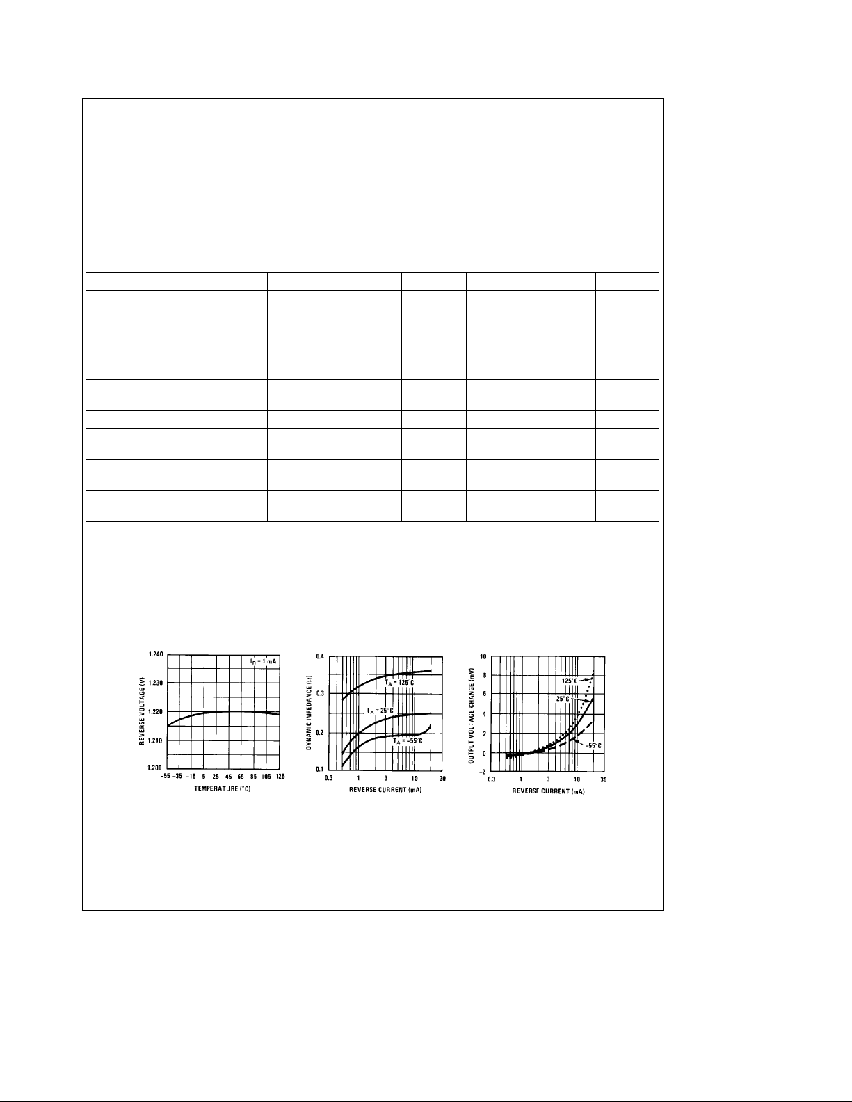
Typical Performance Characteristics
Temperature Drift Reverse Dynamic Impedance Reverse Characteristics
TL/H/5713– 3
2
Page 3

Typical Performance Characteristics (Continued)
Reverse Characteristics Reverse Dynamic Impedance Noise Voltage
Forward Characteristics Response Time Maximum Shunt Capacitance
Typical Applications (Continued)
TL/H/5713– 4
Amplifier Biasing for Constant Gain with Temperature
Thermometer
*Adjust for 0V at 0§C
²
3
Constant Current Source
Adjust for 100 mV/§C
TL/H/5713– 5
Page 4

Physical Dimensions inches (millimeters)
LM113/LM313 Reference Diode
Order Number LM113H, LM113H/883, LM113-1H, LM113-1H/883,
LM113-2H, LM113-2H/883 or LM313H
NS Package Number H02A
LIFE SUPPORT POLICY
NATIONAL’S PRODUCTS ARE NOT AUTHORIZED FOR USE AS CRITICAL COMPONENTS IN LIFE SUPPORT
DEVICES OR SYSTEMS WITHOUT THE EXPRESS WRITTEN APPROVAL OF THE PRESIDENT OF NATIONAL
SEMICONDUCTOR CORPORATION. As used herein:
1. Life support devices or systems are devices or 2. A critical component is any component of a life
systems which, (a) are intended for surgical implant support device or system whose failure to perform can
into the body, or (b) support or sustain life, and whose be reasonably expected to cause the failure of the life
failure to perform, when properly used in accordance support device or system, or to affect its safety or
with instructions for use provided in the labeling, can effectiveness.
be reasonably expected to result in a significant injury
to the user.
National Semiconductor National Semiconductor National Semiconductor National Semiconductor
Corporation Europe Hong Kong Ltd. Japan Ltd.
1111 West Bardin Road Fax: (
Arlington, TX 76017 Email: cnjwge@tevm2.nsc.com Ocean Centre, 5 Canton Rd. Fax: 81-043-299-2408
Tel: 1(800) 272-9959 Deutsch Tel: (
Fax: 1(800) 737-7018 English Tel: (
National does not assume any responsibility for use of any circuitry described, no circuit patent licenses are implied and National reserves the right at any time without notice to change said circuitry and specifications.
Fran3ais Tel: (
Italiano Tel: (
a
49) 0-180-530 85 86 13th Floor, Straight Block, Tel: 81-043-299-2309
a
49) 0-180-530 85 85 Tsimshatsui, Kowloon
a
49) 0-180-532 78 32 Hong Kong
a
49) 0-180-532 93 58 Tel: (852) 2737-1600
a
49) 0-180-534 16 80 Fax: (852) 2736-9960
 Loading...