

Page 1
查询AU211供应商
INTEGRATED CIRCUITS
AU211/LM111/211/311/311B
Voltage comparator
Product data
Supersedes data of 2001 Aug 03
2003 Sep 30
Page 2
Philips Semiconductors Product data
AU21 1/LM11 1/211/31 1/311BVoltage comparator
DESCRIPTION
The LM111 series are voltage comparators that have input currents
approximately a hundred times lower than devices like the µA710.
They are designed to operate over a wider range of supply voltages;
from standard ±15 V op amp supplies down to a single 3 V supply.
Their output is compatible with RTL, DTL, and TTL as well as MOS
circuits. Further, they can drive lamps or relays, switching voltages
up to 50 V at currents as high as 50mA.
Both the inputs and the outputs of the LM111 series can be isolated
from system ground, and the output can drive loads referred to
ground, the positive supply, or the negative supply. Offset balancing
and strobe capability are provided and outputs can be wire-ORed.
Although slower than the µA710 (200 ns response time versus 40 ns),
the devices are also much less prone to spurious oscillations. The
LM111 series has the same pin configuration as the µA710 series.
FEA TURES
•Operates from single 3 V supply (LM311B)
•Maximum input bias current: 150 nA (LM311: 250 nA)
•Maximum offset current: 20 nA (LM311: 50 nA)
•Differential input voltage range: ±30 V
•Power consumption: 135 mW at ±15 V
•High sensitivity: 200 V/mV
•Zero crossing detector
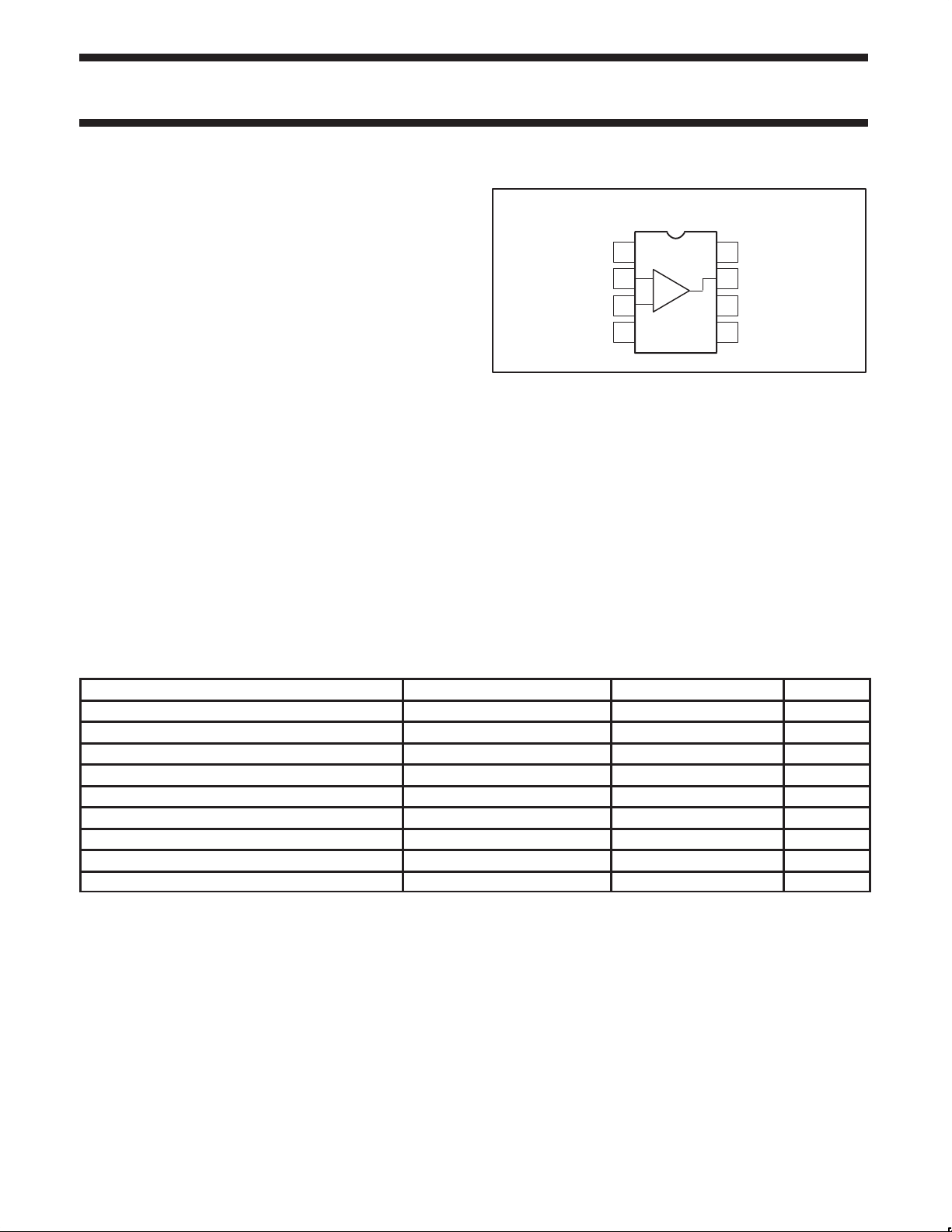
PIN CONFIGURATION
D, N Packages
1
GND
2
INPUT
INPUT
V–
Figure 1. Pin Configuration
+
–
3
45
APPLICATIONS
•Precision squarer
•Positive/negative peak detector
•Low voltage adjustable reference supply
•Switching power amplifier
8
V+
7
OUTPUT
6
BAL/STROBE
BALANCE
SL00062
ORDERING INFORMATION
DESCRIPTION TEMPERATURE RANGE ORDER CODE DWG #
8-Pin Plastic Small Outline Package (SO) –40 °C to +125 °C AU211D SOT96-1
8-Pin Plastic Small Outline Package (SO) –55 °C to +125 °C LM111D SOT96-1
8-Pin Plastic Dual In-Line Package (DIP) –55 °C to +125 °C LM111N SOT97-1
8-Pin Plastic Small Outline Package (SO) –25 °C to +85 °C LM211D SOT96-1
8-Pin Plastic Dual In-Line Package (DIP) –25 °C to +85 °C LM211N SOT97-1
8-Pin Plastic Small Outline Package (SO) 0 °C to +70 °C LM311D SOT96-1
8-Pin Plastic Dual In-Line Package (DIP) 0 °C to +70 °C LM311N SOT97-1
8-Pin Plastic Small Outline Package (SO) 0 °C to +70 °C LM311BD SOT96-1
8-Pin Plastic Dual In-Line Package (DIP) 0 °C to +70 °C LM311BN SOT97-1
2003 Sep 30
2
Page 3

Philips Semiconductors Product data
2
AU211/LM1 11/211/311/311BVoltage comparator
EQUIVALENT SCHEMATIC
BALANCE/
STROBE
BALANCE
V+
INPUTS
R3
300
Q1
Q5
R1
1.3 kΩ
D1
5 VD25 V
R4
300
Q2
R2
1.3 kΩ
R8
750
Q8
R5
70
R6
1.2 kΩR71.2 kΩ
Q3
Q4
Q23
R19
250
Q7
Q8
Q2
R18
200
Q9
Q22
Q10
R17
60
R14
2 kΩ
Figure 2. Equivalent Schematic
Q11
Q19
R9
600
R15
400
R15
450
Q17
Q18
Q20
R10
4 kΩ
Q18
Q13
Q14
V–
Q12
R11
130
R12
600
Q15
R13
4
OUTPUT
SL00063
ABSOLUTE MAXIMUM RATINGS
SYMBOL PARAMETER RATING UNIT
V
S
V
IN
P
D MAX
I Output short-circuit duration 10 sec
T
amb
T
stg
T
sld
NOTES:
1. This rating applies for ±15 V supplies. The positive input voltage limit is 30 V above the negative supply. The negative input voltage limit is
equal to the negative supply voltage or 30 V below the positive supply, whichever is less.
2. Derate above 25 °C, at the following rates:
Total supply voltage 36 V
Output to negative supply voltage
LM111/LM211 50 V
LM311/LM311B 40 V
Ground to negative supply voltage 30 V
Differential input voltage ±30 V
Input voltage
Maximum power dissipation, T
1
= 25 °C (still-air)
amb
N package 1190 mW
±15 V
D package 780 mW
Operating ambient temperature range
AU211 –40 to +125 °C
LM111 –55 to +125 °C
LM211 –25 to +85 °C
LM311/LM311B 0 to +70 °C
Storage temperature range –65 to +150 °C
Lead soldering temperature (10 sec max) 230 °C
N package at 9.5 mW/°C
D package at 6.2 m/W°C
2003 Sep 30
3
Page 4

Philips Semiconductors Product data
AU211/LM1 11/211/311/311BVoltage comparator
DC ELECTRICAL CHARACTERISTICS
1, 2, 3, 6
Over temperature range unless otherwise specified.
SYMBOL
PARAMETER TEST CONDITIONS
AU211
LM111/LM211
LM311 LM311B
UNIT
Min Typ Max Min Typ Max Min Typ Max
T
= 25 °C;
V
I
OS
I
BIAS
A
OS
V
Input offset voltage
Input offset current
3
3
Input bias current T
Voltage gain T
Response time
4
amb
R
≤ 50 kΩ
S
T
= 25 °C 4.0 10 6.0 50 6 25 nA
amb
= 25 °C 60 100 100 250 100 200 nA
amb
= 25 °C 200 200 200 V/mV
amb
T
= 25 °C 200 200 500 ns
amb
0.7 3.0 2.0 7.5 2.0 7.5 mV
LM111/211 VIN ≤ –5mV;
= 50 mA
I
OUT
V
SAT
I
BAL/STR
Saturation voltage
Strobe on current T
LM31 1/B V
I
OUT
T
amb
amb
≤ –10 mV ;
IN
0.75 1.5 0.75 1.5 0.75 1.5 V
= 50 mA
= 25 °C
= 25 °C 3.0 3.0 3.0 mA
LM111/211 VIN ≥ 5 mV;
V
= 35 V
OUT
≥ 10 mV;
IN
V
T
amb
= 35 V
OUT
= 25 °C,
0.2 10 0.2 50 0.2 50 nA
= 3 mA
= –5 V)
GND
RS ≤ 50 kΩ 4.0 10 10 mV
20 70 50 nA
go to 5 V)
–14.5
13.8
to
–14.7
13.0 –14.5
13.8
to
–14.7
13.0
V–
+0.5
V+
–1.5
I
LEAKAGE
V
OS
I
OS
I
BIAS
V
IN
LM31 1/B V
Output leakage current
6
I
STROBE
(V– = V
Input offset voltage
Input offset current
3
3
Input bias current 150 300 250 nA
Input voltage range
V = ±15 V (Pin 7 may
V+ ≥ 4.5 V, V– = 0 V
LM111/211 V
V
OL
Saturation voltage
6
I
LM31 1/B V
I
I
OH
I
CC
I
EE
Output leakage current
Positive supply current T
Negative supply voltage T
V
≤ –6 mV;
IN
≤ 8 mA
SINK
≤ –10 mV;
IN
≤ 8 mA
SINK
VIN ≥ 5 mV;
= 35 V
OUT
= 25 °C 5.1 6.0 5.1 7.5 1.6 3.5 mA
amb
= 25 °C 4.1 5.0 4.1 5.0 mA
amb
0.23 0.4 0.23 0.4 0.23 0.4 V
0.1 0.5 µA
NOTES:
1. This rating applies for ±15 V supplies. The positive input voltage limit is 30 V above the negative supply. The negative input voltage limit is
equal to the negative supply voltage or 30 V below the positive supply, whichever is less.
2. These specifications apply for VS = ±15 V and 0 °C < T
specifications are limited to –25 °C ≤ T
–55 °C < T
supply up to ±15 V supplies.
< +125 °C. The offset voltage, offset current, and bias current specifications apply for any supply voltage from a single 5 V
amb
≤ +85 °C, for the AU211 is limited to –40 °C < T
amb
< 70 °C unless otherwise specified. With the LM211, however, all temperature
amb
< +125 °C, and for the LM111 is limited to
amb
3. The offset voltages and offset currents given are the maximum values required to drive the output within a volt of either supply with 1 mA
load. Thus, these parameters define an error band and take into account the worst case effects of voltage gain and input impedance.
4. The response time specified is for a 100 mV input step with 5 mV over-drive.
5. Do not short the strobe pin to ground; it should be current driven at 3 mA to 5 mA.
6. LM31 1B, all parameters are at V+ = 3 V ±10%; V– = GND = 0 V.
V
2003 Sep 30
4
Page 5

Philips Semiconductors Product data
AU211/LM1 11/211/311/311BVoltage comparator
TYPICAL APPLICATIONS
BAL
R2
3 kΩ
R1
5
3 kΩ
2
6
INPUT
* Values shown are for a 0 to 30 V logic swing and a 15 V threshold.
** May be added to control speed and reduce susceptibility to noise spikes.
+
LM311
3
–
1
4
V– = 10V
V+ = 5 V
8
7
R3
10 kΩ
TO
MOS
LOGIC
R2
1 kΩ
MAGNETIC
PICKUP
R1
4.5 kΩ
V+ 5 V
R3
2 kΩ
INPUT
R1
240 kΩ
C1
8
2
+
LM311
–
3
7
TTL
1
4
OUTPUT
R2
47 kΩ
82 kΩ
R3
2
8
+
LM311
3
–
4
R4
82 kΩ
V+ = 5 V
R5
1 kΩ
7
1
TO TTL
OUTPUT
Zero Detector
Driving MOS Logic
Detector for Magnetic
Transducer
Figure 3. Typical Applications
TTL Interface with
High Level Logic
SL00064
2003 Sep 30
5
Page 6

Philips Semiconductors Product data
AU211/LM1 11/211/311/311BVoltage comparator
DIP8: plastic dual in-line package; 8 leads (300 mil) SOT97-1
2003 Sep 30
6
Page 7

Philips Semiconductors Product data
AU211/LM1 11/211/311/311BVoltage comparator
SO8: plastic small outline package; 8 leads; body width 3.9 mm SOT96-1
2003 Sep 30
7
Page 8

Philips Semiconductors Product data
AU211/LM1 11/211/311/311BVoltage comparator
REVISION HISTORY
Rev Date Description
_3 20030930 Product data (9397 750 12106). ECN 853-0927 30378 of 26 September 2003.
_2 20010803 Product data (9397 750 09216). ECN 853-0927 26834 of 03 August 2001. Supersedes data of 1994 Aug 31.
Data sheet status
Level
I
Data sheet status
Objective data
Replaces LM111_211_311_311B_2 (9397 750 09216) of 2001 Aug 03.
Modifications:
•Add Type number AU211.
•DC electrical characteristics, Note 2, on page 4: add “for the AU211 is limited to –40 °C < T
[1]
Product
[2] [3]
status
Development
Definitions
This data sheet contains data from the objective specification for product development.
Philips Semiconductors reserves the right to change the specification in any manner without notice.
< +125 °C”.
amb
II
III
[1] Please consult the most recently issued data sheet before initiating or completing a design.
[2] The product status of the device(s) described in this data sheet may have changed since this data sheet was published. The latest information is available on the Internet at URL
[3] For data sheets describing multiple type numbers, the highest-level product status determines the data sheet status.
Preliminary data
Product data
http://www.semiconductors.philips.com.
Qualification
Production
This data sheet contains data from the preliminary specification. Supplementary data will be published
at a later date. Philips Semiconductors reserves the right to change the specification without notice, in
order to improve the design and supply the best possible product.
This data sheet contains data from the product specification. Philips Semiconductors reserves the
right to make changes at any time in order to improve the design, manufacturing and supply. Relevant
changes will be communicated via a Customer Product/Process Change Notification (CPCN).
Definitions
Short-form specification — The data in a short-form specification is extracted from a full data sheet with the same type number and title. For detailed information see
the relevant data sheet or data handbook.
Limiting values definition — Limiting values given are in accordance with the Absolute Maximum Rating System (IEC 60134). Stress above one or more of the limiting
values may cause permanent damage to the device. These are stress ratings only and operation of the device at these or at any other conditions above those given
in the Characteristics sections of the specification is not implied. Exposure to limiting values for extended periods may affect device reliability.
Application information — Applications that are described herein for any of these products are for illustrative purposes only. Philips Semiconductors make no
representation or warranty that such applications will be suitable for the specified use without further testing or modification.
Disclaimers
Life support — These products are not designed for use in life support appliances, devices, or systems where malfunction of these products can reasonably be
expected to result in personal injury . Philips Semiconductors customers using or selling these products for use in such applications do so at their own risk and agree
to fully indemnify Philips Semiconductors for any damages resulting from such application.
Right to make changes — Philips Semiconductors reserves the right to make changes in the products—including circuits, standard cells, and/or software—described
or contained herein in order to improve design and/or performance. When the product is in full production (status ‘Production’), relevant changes will be communicated
via a Customer Product/Process Change Notification (CPCN). Philips Semiconductors assumes no responsibility or liability for the use of any of these products, conveys
no license or title under any patent, copyright, or mask work right to these products, and makes no representations or warranties that these products are free from patent,
copyright, or mask work right infringement, unless otherwise specified.
Contact information
For additional information please visit
http://www.semiconductors.philips.com . Fax: +31 40 27 24825
For sales offices addresses send e-mail to:
sales.addresses@www.semiconductors.philips.com.
Document order number: 9397 750 12106
Koninklijke Philips Electronics N.V. 2003
All rights reserved. Printed in U.S.A.
Date of release: 09-03
2003 Sep 30
8
 Loading...