

Page 1
September 2007
LM3102
SIMPLE SWITCHER® Synchronous 1MHz 2.5A
Step-Down Voltage Regulator
General Description
The LM3102 Synchronously Rectified Buck Converter features all required functions to implement a highly efficient and
cost effective buck regulator. It is capable of supplying 2.5A
to loads with an output voltage as low as 0.8V. Dual N-Channel synchronous MOSFET switches allow a low component
count, thus reducing complexity and minimizing board size.
Different from most other COT regulators, the LM3102 does
not rely on output capacitor ESR for stability, and is designed
to work exceptionally well with ceramic and other very low
ESR output capacitors. It requires no loop compensation, results in a fast load transient response and simple circuit
implementation. The operating frequency remains nearly constant with line variations due to the inverse relationship between the input voltage and the on-time. The operating
frequency can be externally programmed up to 1 MHz. Protection features include VCC under-voltage lock-out, output
over-voltage protection, thermal shutdown, and gate drive
under-voltage lock-out. The LM3102 is available in the thermally enhanced eTSSOP-20 package.
Key Specifications
■
Input voltage range 4.5V-42V
■
2.5A output current
■
0.8V, ±1.5% reference
■
Integrated dual N-Channel main and synchronous
MOSFETs
■
Thermally enhanced eTSSOP-20 package
Features
■
Low component count and small solution size
■
Stable with ceramic and other low ESR capacitors
■
No loop compensation required
■
High efficiency at a light load by DCM operation
■
Pre-bias startup
■
Ultra-fast transient response
■
Programmable soft-start
■
Programmable switching frequency up to 1 MHz
■
Valley current limit
■
Output over-voltage protection
■
Precision internal reference for an adjustable output
voltage down to 0.8V
■
Thermal shutdown
Typical Applications
■
5VDC, 12VDC, 24VDC, 12VAC, and 24VAC systems
■
Embedded Systems
■
Industrial Control
■
Automotive Telematics and Body Electronics
■
Point of Load Regulators
■
Storage Systems
■
Broadband Infrastructure
■
Direct Conversion from 2/3/4 Cell Lithium Batteries
Systems
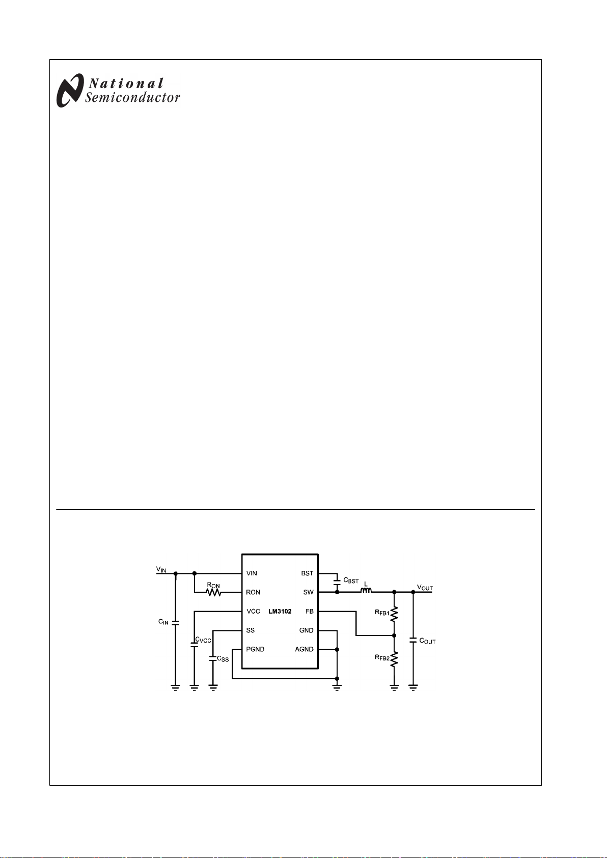
Typical Application
30021301
SIMPLE SWITCHER® is a registered trademark of National Semiconductor Corporation
© 2007 National Semiconductor Corporation 300213 www.national.com
LM3102 SIMPLE SWITCHER® Synchronous 1MHz 2.5A Step-Down Voltage Regulator
Page 2
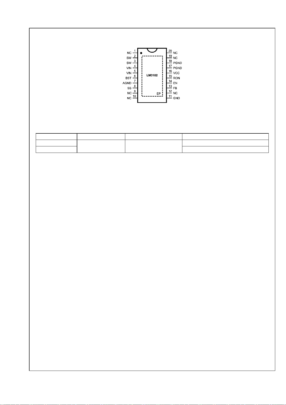
Connection Diagram
30021302
20-lead Plastic eTSSOP
NS Package Number MXA20A
Ordering Information
Order Number Package Type NSC Package Drawing Supplied As
LM3102MH Exposed Pad TSSOP-20 MXA0020 73 units per Anti-Static Tube
LM3102MHX 2500 Units on Tape and Reel
www.national.com 2
LM3102
Page 3
Pin Descriptions
Pin Name Description Application Information
1,9,10,12,19,20 N/C No Connection These pins must be left unconnected.
2, 3 SW Switching Node Internally connected to the source of the main
MOSFET and the drain of the Synchronous MOSFET.
Connect to the inductor.
4, 5 VIN Input supply voltage Supply pin to the device. Nominal input range is 4.5V
to 42V.
6 BST Connection for bootstrap capacitor Connect a 33 nF capacitor from the SW pin to this pin.
An internal diode charges the capacitor during the main
MOSFET off-time.
7 AGND Analog Ground Ground for all internal circuitry other than the PGND
pin.
8 SS Soft-start An 8 µA internal current source charges an external
capacitor to provide the soft- start function.
11 GND Ground Must be connected to the AGND pin for normal
operation. The GND and AGND pins are not internally
connected.
13 FB Feedback Internally connected to the regulation and over-voltage
comparators. The regulation setting is 0.8V at this pin.
Connect to feedback resistors.
14 EN Enable pin Connect a voltage higher than 1.26V to enable the
regulator.
15 RON On-time Control An external resistor from the VIN pin to this pin sets the
main MOSFET on-time.
16 VCC Start-up regulator Output Nominally regulated to 6V. Connect a capacitor of not
less than 680 nF between the VCC and AGND pins for
stable operation.
17, 18 PGND Power Ground Synchronous MOSFET source connection. Tie to a
ground plane.
DAP EP Exposed Pad Thermal connection pad. Connect to the ground plane.
3 www.national.com
LM3102
Page 4
Absolute Maximum Ratings (Note 1)
If Military/Aerospace specified devices are required,
please contact the National Semiconductor Sales Office/
Distributors for availability and specifications.
VIN, RON to AGND -0.3V to 43.5V
SW to AGND -0.3V to 43.5V
SW to AGND (Transient) -2V (< 100ns)
VIN to SW -0.3V to 43.5V
BST to SW -0.3V to 7V
All Other Inputs to AGND -0.3V to 7V
ESD Rating (Note 2)
Human Body Model ±2kV
Storage Temperature Range -65°C to +150°C
Junction Temperature (TJ) 150°C
Operating Ratings (Note 1)
Supply Voltage Range (VIN) 4.5V to 42V
Junction Temperature Range (TJ)
−40°C to +125°C
Thermal Resistance (θJC) (Note 3)
6.5°C/W
Electrical Characteristics Specifications with standard type are for T
J
= 25°C only; limits in boldface type apply
over the full Operating Junction Temperature (TJ) range. Minimum and Maximum limits are guaranteed through test, design, or
statistical correlation. Typical values represent the most likely parametric norm at TJ = 25°C, and are provided for reference
purposes only. Unless otherwise stated the following conditions apply: VIN = 18V, V
OUT
= 3.3V.
Symbol Parameter Conditions Min Typ Max Units
Start-Up Regulator, V
CC
V
CC
VCC output voltage CCC = 680nF, no load 5.0 6.0 7.2 V
VIN - V
CC
V
IN
- VCC dropout voltage ICC = 2mA 50 200 mV
ICC = 20mA 350 570
I
VCCL
VCC current limit (Note 4) VCC = 0V 40 65 mA
V
CC-UVLO
VCC under-voltage lockout threshold
(UVLO)
VIN increasing 3.6 3.75 3.9 V
V
CC-UVLO-HYS
VCC UVLO hysteresis VIN decreasing 130 mV
t
VCC-UVLO-D
VCC UVLO filter delay 3 µs
I
IN
IIN operating current No switching, VFB = 1V 0.7 1 mA
I
IN-SD
IIN operating current, Device shutdown VEN = 0V 25 40 µA
Switching Characteristics
R
DS-UP-ON
Main MOSFET R
DS(on)
0.18 0.375
Ω
R
DS- DN-ON
Syn. MOSFET R
DS(on)
0.11 0.225
Ω
V
G-UVLO
Gate drive voltage UVLO V
BST
- VSW increasing 3.3 4 V
Soft-start
I
SS
SS pin source current VSS = 0.5V 6 8 10 µA
Current Limit
I
CL
Syn. MOSFET current limit threshold 2.7 A
ON/OFF Timer
t
on
ON timer pulse width
VIN = 10V, RON = 100 kΩ
1.38 µs
VIN = 30V, RON = 100 kΩ
0.47
t
on-MIN
ON timer minimum pulse width 150 ns
t
off
OFF timer pulse width 260 ns
Enable Input
V
EN
EN Pin input threshold VEN rising 1.13 1.18 1.23 V
V
EN-HYS
Enable threshold hysteresis VEN falling 90 mV
Regulation and Over-Voltage Comparator
V
FB
In-regulation feedback voltage
VSS ≥ 0.8V
TJ = −40°C to +125°C
0.784 0.8 0.816 V
VSS ≥ 0.8V
TJ = 0°C to +125°C
0.788 0.812
V
FB-OV
Feedback over-voltage threshold 0.888 0.920 0.945 V
I
FB
5 nA
www.national.com 4
LM3102
Page 5
Symbol Parameter Conditions Min Typ Max Units
Thermal Shutdown
T
SD
Thermal shutdown temperature TJ rising 165 °C
T
SD-HYS
Thermal shutdown temperature
hysteresis
TJ falling 20 °C
Note 1: Absolute Maximum Ratings are limits beyond which damage to the device may occur. Operating Ratings are conditions under which operation of the
device is intended to be functional. For guaranteed specifications and test conditions, see the Electrical Characteristics.
Note 2: The human body model is a 100pF capacitor discharged through a 1.5kΩ resistor into each pin.
Note 3: θJC measurements are performed in general accordance with Mil-Std 883B, Method 1012.1 and utilizes the copper heat sink technique. Copper Heat
Sink @ 60°C.
Note 4: VCC provides self bias for the internal gate drive and control circuits. Device thermal limitations limit external loading.
5 www.national.com
LM3102
Page 6
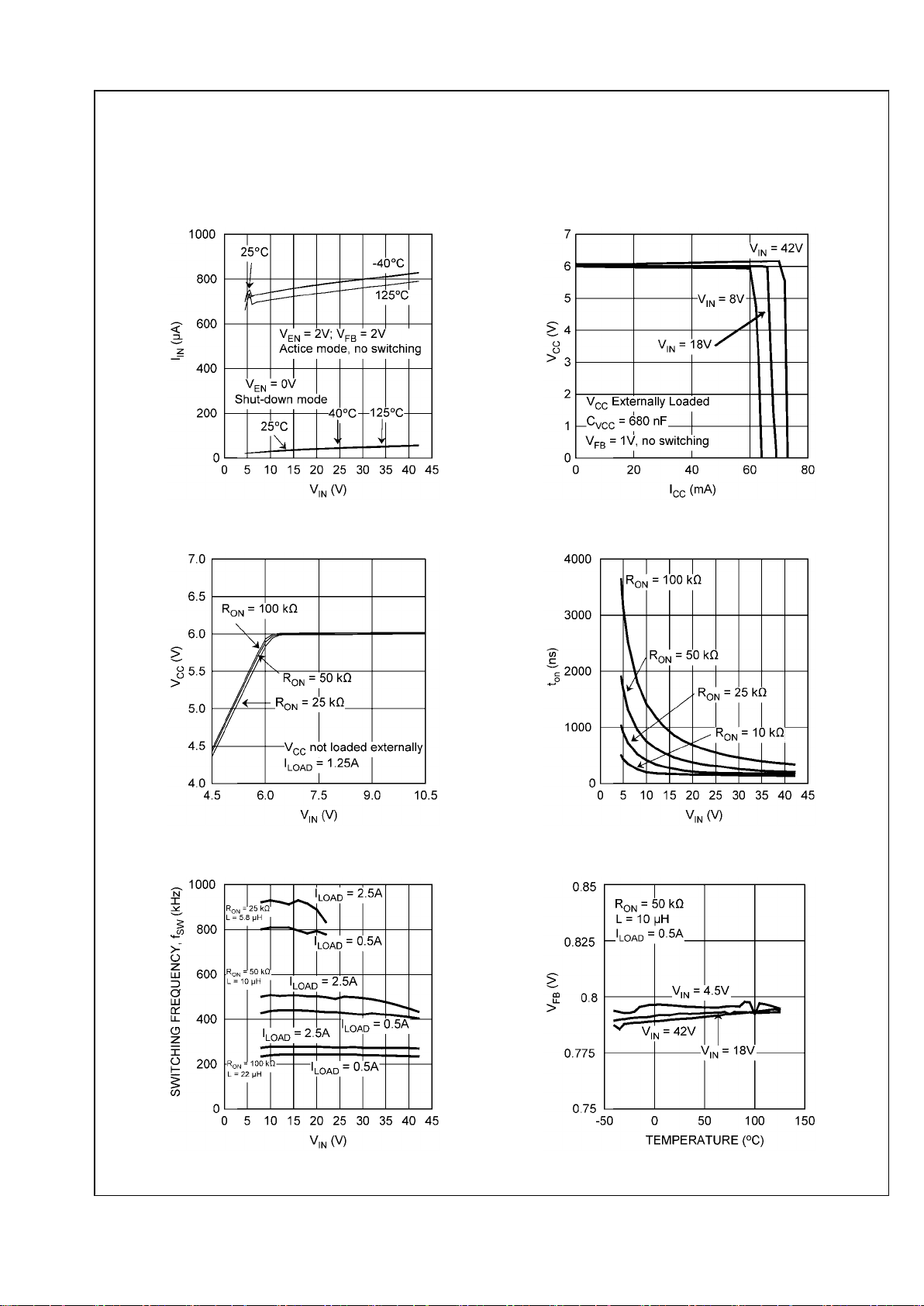
Typical Performance Characteristics
All curves are taken at VIN = 18V with the configuration in the typical application circuit for V
OUT
= 3.3V shown in this datasheet.
TA = 25°C, unless otherwise specified.
Quiescent Current, IIN vs V
IN
30021303
VCC vs I
CC
30021304
VCC vs V
IN
30021305
ton vs V
IN
30021306
Switching Frequency, fSW vs V
IN
30021307
VFB vs Temperature
30021308
www.national.com 6
LM3102
Page 7

R
DS(on)
vs Temperature
30021309
Efficiency vs Load Current
(V
OUT
= 3.3V)
30021310
V
OUT
Regulation vs Load Current
(V
OUT
= 3.3V)
30021311
Efficiency vs Load Current
(V
OUT
= 0.8V)
30021312
V
OUT
Regulation vs Load Current
(V
OUT
= 0.8V)
30021313
Power Up
(V
OUT
= 3.3V, 2.5A Loaded)
30021339
7 www.national.com
LM3102
Page 8

Enable Transient
(V
OUT
= 3.3V, 2.5A Loaded)
30021314
Shutdown Transient
(V
OUT
= 3.3V, 2.5A Loaded)
30021315
Continuous Mode Operation
(V
OUT
= 3.3V, 2.5A Loaded)
30021316
Discontinuous Mode Operation
(V
OUT
= 3.3V, 0.025A Loaded)
30021317
DCM to CCM Transition
(V
OUT
= 3.3V, 0.15A - 2.5A Load)
30021318
Load Transient
(V
OUT
= 3.3V, 0.25A - 2.5A Load, Current slew-rate: 2.5A/µs)
30021319
www.national.com 8
LM3102
Page 9

Simplified Functional Block Diagram
30021320
9 www.national.com
LM3102
Page 10

Functional Description
The LM3102 Step Down Switching Regulator features all required functions to implement a cost effective, efficient buck
power converter capable of supplying 2.5A to a load. It contains Dual N-Channel main and synchronous MOSFETs. The
Constant ON-Time (COT) regulation scheme requires no loop
compensation, results in fast load transient response and
simple circuit implementation. The regulator can function
properly even with an all ceramic output capacitor network,
and does not rely on the output capacitor’s ESR for stability.
The operating frequency remains constant with line variations
due to the inverse relationship between the input voltage and
the on-time. The valley current limit detection circuit, with the
limit set internally at 2.7A, inhibits the main MOSFET until the
inductor current level subsides.
The LM3102 can be applied in numerous applications and
can operate efficiently for inputs as high as 42V. Protection
features include output over-voltage protection, thermal shutdown, VCC under-voltage lock-out, gate drive under-voltage
lock-out. The LM3102 is available in the thermally enhanced
eTSSOP-20 package.
COT Control Circuit Overview
COT control is based on a comparator and a one-shot ontimer, with the output voltage feedback (feeding to the FB pin)
compared with an internal reference of 0.8V. If the voltage of
the FB pin is below the reference, the main MOSFET is turned
on for a fixed on-time determined by a programming resistor
RON and the input voltage VIN, upon which the on-time varies
inversely. Following the on-time, the main MOSFET remains
off for a minimum of 260 ns. Then, if the voltage of the FB pin
is below the reference, the main MOSFET is turned on again
for another on-time period. The switching will continue to
achieve regulation.
The regulator will operate in the discontinuous conduction
mode (DCM) at a light load, and the continuous conduction
mode (CCM) with a heavy load. In the DCM, the current
through the inductor starts at zero and ramps up to a peak
during the on-time, and then ramps back to zero before the
end of the off-time. It remains zero and the load current is
supplied entirely by the output capacitor. The next on-time
period starts when the voltage at the FB pin falls below the
internal reference. The operating frequency in the DCM is
lower and varies larger with the load current as compared with
the CCM. Conversion efficiency is maintained since conduction loss and switching loss are reduced with the reduction in
the load and the switching frequency respectively. The operating frequency in the DCM can be calculated approximately
as follows:
(1)
In the continuous conduction mode (CCM), the current flows
through the inductor in the entire switching cycle, and never
reaches zero during the off-time. The operating frequency remains relatively constant with load and line variations. The
CCM operating frequency can be calculated approximately as
follows:
(2)
The output voltage is set by two external resistors R
FB1
and
R
FB2
. The regulated output voltage is
V
OUT
= 0.8V x (R
FB1
+ R
FB2
)/R
FB2
(3)
Startup Regulator (VCC)
A startup regulator is integrated within the LM3102. The input
pin VIN can be connected directly to a line voltage up to 42V.
The VCC output regulates at 6V, and is current limited to 65
mA. Upon power up, the regulator sources current into an external capacitor C
VCC
, which is connected to the VCC pin. For
stability, C
VCC
must be at least 680 nF. When the voltage on
the VCC pin is higher than the under-voltage lock-out (UVLO)
threshold of 3.75V, the main MOSFET is enabled and the SS
pin is released to allow the soft-start capacitor CSS to charge.
The minimum input voltage is determined by the dropout voltage of the regulator and the VCC UVLO falling threshold
(≊3.7V). If VIN is less than ≊4.0V, the regulator shuts off and
VCC goes to zero.
Regulation Comparator
The feedback voltage at the FB pin is compared to a 0.8V
internal reference. In normal operation (the output voltage is
regulated), an on-time period is initiated when the voltage at
the FB pin falls below 0.8V. The main MOSFET stays on for
the on-time, causing the output voltage and consequently the
voltage of the FB pin to rise above 0.8V. After the on-time
period, the main MOSFET stays off until the voltage of the FB
pin falls below 0.8V again. Bias current at the FB pin is nominally 5 nA.
Zero Coil Current Detect
The current of the synchronous MOSFET is monitored by a
zero coil current detection circuit which inhibits the synchronous MOSFET when its current reaches zero until the
next on-time. This circuit enables the DCM operation, which
improves the efficiency at a light load.
Over-Voltage Comparator
The voltage at the FB pin is compared to a 0.92V internal
reference. If it rises above 0.92V, the on-time is immediately
terminated. This condition is known as over-voltage protection (OVP). It can occur if the input voltage or the output load
changes suddenly. Once the OVP is activated, the main
MOSFET remains off until the voltage at the FB pin falls below
0.92V. The synchronous MOSFET will stay on to discharge
the inductor until the inductor current reduces to zero, and
then switch off.
ON-Time Timer, Shutdown
The on-time of the LM3102 main MOSFET is determined by
the resistor RON and the input voltage VIN. It is calculated as
follows:
(4)
The inverse relationship of ton and VIN gives a nearly constant
frequency as VIN is varied. RON should be selected such that
the on-time at maximum VIN is greater than 150 ns. The ontimer has a limiter to ensure a minimum of 150 ns for ton. This
limits the maximum operating frequency, which is governed
by the following equation:
www.national.com 10
LM3102
Page 11

(5)
The LM3102 can be remotely shutdown by pulling the voltage
of the EN pin below 1V. In this shutdown mode, the SS pin is
internally grounded, the on-timer is disabled, and bias currents are reduced. Releasing the EN pin allows normal operation to resume because the EN pin is internally pulled up.
30021325
FIGURE 1. Shutdown Implementation
Current Limit
Current limit detection is carried out during the off-time by
monitoring the re-circulating current through the synchronous
MOSFET. Referring to the Functional Block Diagram, when
the main MOSFET is turned off, the inductor current flows
through the load, the PGND pin and the internal synchronous
MOSFET. If this current exceeds 2.7A, the current limit comparator toggles, and as a result disabling the start of the next
on-time period. The next switching cycle starts when the recirculating current falls back below 2.7A (and the voltage at
the FB pin is below 0.8V). The inductor current is monitored
during the on-time of the synchronous MOSFET. As long as
the inductor current exceeds 2.7A, the main MOSFET will remain inhibited to achieve current limit. The operating frequency is lower during current limit due to a longer off-time.
Figure 2 illustrates an inductor current waveform. On average, the output current I
OUT
is the same as the inductor
current IL, which is the average of the rippled inductor current.
In case of current limit (the current limit portion of Figure 2),
the next on-time will not initiate until that the current drops
below 2.7A (assume the voltage at the FB pin is lower than
0.8V). During each on-time the current ramps up an amount
equal to:
(6)
During current limit, the LM3102 operates in a constant current mode with an average output current I
OUT(CL)
equal to
2.7A + ILR / 2.
30021326
FIGURE 2. Inductor Current - Current Limit Operation
11 www.national.com
LM3102
Page 12

N-Channel MOSFET and Driver
The LM3102 integrates an N-Channel main MOSFET and an
associated floating high voltage main MOSFET gate driver.
The gate drive circuit works in conjunction with an external
bootstrap capacitor C
BST
and an internal high voltage diode.
C
BST
connecting between the BST and SW pins powers the
main MOSFET gate driver during the main MOSFET on-time.
During each off-time, the voltage of the SW pin falls to approximately -1V, and C
BST
charges from VCC through the
internal diode. The minimum off-time of 260 ns provides
enough time for charging C
BST
in each cycle.
Soft-Start
The soft-start feature allows the converter to gradually reach
a steady state operating point, thereby reducing startup
stresses and current surges. Upon turn-on, after VCC reaches
the under-voltage threshold, an 8 µA internal current source
charges up an external capacitor CSS connecting to the SS
pin. The ramping voltage at the SS pin (and the non-inverting
input of the regulation comparator as well) ramps up the output voltage V
OUT
in a controlled manner.
An internal switch grounds the SS pin if any of the following
three cases happens: (i) VCC is below the under-voltage lockout threshold; (ii) a thermal shutdown occurs; or (iii) the EN
pin is grounded. Alternatively, the output voltage can be shut
off by connecting the SS pin to ground using an external
switch. Releasing the switch allows the SS pin to ramp up and
the output voltage to return to normal. The shutdown configuration is shown in Figure 3.
30021327
FIGURE 3. Alternate Shutdown Implementation
Thermal Protection
The junction temperature of the LM3102 should not exceed
the maximum limit. Thermal protection is implemented by an
internal Thermal Shutdown circuit, which activates (typically)
at 165°C to make the controller enter a low power reset state
by disabling the main MOSFET, disabling the on-timer, and
grounding the SS pin. Thermal protection helps prevent
catastrophic failures from accidental device overheating.
When the junction temperature falls back below 145°C (typical hysteresis = 20°C), the SS pin is released and normal
operation resumes.
Thermal Derating
The LM3102 is capable of supplying 2.5A below an ambient
temperature of 100°C. Under worst case operation, with either input voltage up to 42V, operating frequency up to 1 MHz,
or voltage of the RON pin below the absolute maximum of 7V,
the LM3102 can deliver a minimum of 1.9A output current
without thermal shutdown with a PCB ground plane copper
area of 40cm2, 2 oz/Cu. Figure 4 shows a thermal derating
curve for the minimum output current without thermal shutdown against ambient temperature up to 125°C. Obtaining
2.5A output current is possible by increasing the PCB ground
plane area, or reducing the input voltage or operating frequency.
30021340
FIGURE 4. Thermal Derating Curve
www.national.com 12
LM3102
Page 13

Applications Information
EXTERNAL COMPONENTS
The following guidelines can be used to select external components.
R
FB1
and R
FB2
: These resistors should be chosen from stan-
dard values in the range of 1.0 kΩ to 10 kΩ, satisfying the
following ratio:
R
FB1/RFB2
= (V
OUT
/0.8V) - 1 (7)
For V
OUT
= 0.8V, the FB pin can be connected to the output
directly with a pre-load resistor drawing more than 20 µA. It is
because the converter operation needs a minimum inductor
current ripple to maintain good regulation when no load is
connected.
RON: Equation (2) can be used to select RON if a desired op-
erating frequency is selected. But the minimum value of
RON is determined by the minimum on-time. It can be calculated as follows:
(8)
If RON calculated from (2) is smaller than the minimum value
determined in (8), a lower frequency should be selected to recalculate RON by (2). Alternatively, V
IN(MAX)
can also be limited
in order to keep the frequency unchanged. The relationship
of V
IN(MAX)
and RON is shown in Figure 5.
On the other hand, the minimum off-time of 260 ns can limit
the maximum duty ratio. Larger RON should be selected in any
application requiring large duty ratio.
30021329
FIGURE 5. Maximum VIN for selected R
ON
L: The main parameter affected by the inductor is the ampli-
tude of inductor current ripple (ILR). Once ILR is selected, L can
be determined by:
(9)
where VIN is the maximum input voltage and fSW is determined
from (2).
If the output current I
OUT
is determined, by assuming that
I
OUT
= IL, the higher and lower peak of ILR can be determined.
Beware that the higher peak of ILR should not be larger than
the saturation current of the inductor and current limits of the
main and synchronous MOSFETs. Also, the lower peak of
ILR must be positive if CCM operation is required.
30021331
FIGURE 6. Inductor selection for V
OUT
= 3.3V
30021332
FIGURE 7. Inductor selection for V
OUT
= 0.8V
Figure 6 and Figure 7 show curves on inductor selection for
various V
OUT
and RON. For small RON, according to (8), VIN is
limited. Some curves are therefore limited as shown in the
figures.
C
VCC
: The capacitor on the VCC output provides not only noise
filtering and stability, but also prevents false triggering of the
VCC UVLO at the main MOSFET on/off transitions. C
VCC
should be no smaller than 680 nF for stability, and should be
a good quality, low ESR, ceramic capacitor.
C
OUT
and C
OUT3
: C
OUT
should generally be no smaller than
10 µF. Experimentation is usually necessary to determine the
minimum value for C
OUT
, as the nature of the load may require
a larger value. A load which creates significant transients requires a larger C
OUT
than a fixed load.
C
OUT3
is a small value ceramic capacitor located close to the
LM3102 to further suppress high frequency noise at V
OUT
. A
100 nF capacitor is recommended.
13 www.national.com
LM3102
Page 14

CIN and C
IN3
: The function of CIN is to supply most of the main
MOSFET current during the on-time, and limit the voltage ripple at the VIN pin, assuming that the voltage source connecting to the VIN pin has finite output impedance. If the voltage
source’s dynamic impedance is high (effectively a current
source), CIN supplies the average input current, but not the
ripple current.
At the maximum load current, when the main MOSFET turns
on, the current to the VIN pin suddenly increases from zero
to the lower peak of the inductor’s ripple current and ramps
up to the higher peak value. It then drops to zero at turn-off.
The average current during the on-time is the load current.
For a worst case calculation, CIN must be capable of supplying
this average load current during the maximum on-time. CIN is
calculated from:
(10)
where I
OUT
is the load current, ton is the maximum on-time,
and ΔVIN is the allowable ripple voltage at VIN.
C
IN3
’s purpose is to help avoid transients and ringing due to
long lead inductance at the VIN pin. A low ESR 0.1 µF ceramic
chip capacitor located close to the LM3102 is recommended.
C
BST
: A 33 nF high quality ceramic capacitor with low ESR is
recommended for C
BST
since it supplies a surge current to
charge the main MOSFET gate driver at turn-on. Low ESR
also helps ensure a complete recharge during each off-time.
CSS: The capacitor at the SS pin determines the soft-start
time, i.e. the time for the reference voltage at the regulation
comparator and the output voltage to reach their final value.
The time is determined from the following equation:
(11)
CFB: If the output voltage is higher than 1.6V, CFB is needed
in the Discontinuous Conduction Mode to reduce the output
ripple. The recommended value for CFB is 10 nF.
PC BOARD LAYOUT
The LM3102 regulation, over-voltage, and current limit comparators are very fast so they will respond to short duration
noise pulses. Layout is therefore critical for optimum performance. It must be as neat and compact as possible, and all
external components must be as close to their associated
pins of the LM3102 as possible. Refer to the functional block
diagram, the loop formed by CIN, the main and synchronous
MOSFET internal to the LM3102, and the PGND pin should
be as small as possible. The connection from the PGND pin
to CIN should be as short and direct as possible. Vias should
be added to connect the ground of CIN to a ground plane,
located as close to the capacitor as possible. The bootstrap
capacitor C
BST
should be connected as close to the SW and
BST pins as possible, and the connecting traces should be
thick. The feedback resistors and capacitor R
FB1
, R
FB2
, and
CFB should be close to the FB pin. A long trace running from
V
OUT
to R
FB1
is generally acceptable since this is a low
impedance node. Ground R
FB2
directly to the AGND pin (pin
7). The output capacitor C
OUT
should be connected close to
the load and tied directly to the ground plane. The inductor L
should be connected close to the SW pin with as short a trace
as possible to reduce the potential for EMI (electromagnetic
interference) generation. If it is expected that the internal dissipation of the LM3102 will produce excessive junction temperature during normal operation, making good use of the PC
board’s ground plane can help considerably to dissipate heat.
The exposed pad on the bottom of the LM3102 IC package
can be soldered to the ground plane, which should extend out
from beneath the LM3102 to help dissipate heat. The exposed
pad is internally connected to the LM3102 IC substrate. Additionally the use of thick traces, where possible, can help
conduct heat away from the LM3102. Using numerous vias to
connect the die attached pad to the ground plane is a good
practice. Judicious positioning of the PC board within the end
product, along with the use of any available air flow (forced or
natural convection) can help reduce the junction temperature.
30021335
Typical Application Schematic for V
OUT
= 3.3V
www.national.com 14
LM3102
Page 15

30021336
Typical Application Schematic for V
OUT
= 0.8V
15 www.national.com
LM3102
Page 16

Physical Dimensions inches (millimeters) unless otherwise noted
20-Lead Plastic eTSSOP Package
NS Package Number MXA20A
www.national.com 16
LM3102
Page 17

Notes
17 www.national.com
LM3102
Page 18

Notes
LM3102 SIMPLE SWITCHER® Synchronous 1MHz 2.5A Step-Down Voltage Regulator
THE CONTENTS OF THIS DOCUMENT ARE PROVIDED IN CONNECTION WITH NATIONAL SEMICONDUCTOR CORPORATION
(“NATIONAL”) PRODUCTS. NATIONAL MAKES NO REPRESENTATIONS OR WARRANTIES WITH RESPECT TO THE ACCURACY
OR COMPLETENESS OF THE CONTENTS OF THIS PUBLICATION AND RESERVES THE RIGHT TO MAKE CHANGES TO
SPECIFICATIONS AND PRODUCT DESCRIPTIONS AT ANY TIME WITHOUT NOTICE. NO LICENSE, WHETHER EXPRESS,
IMPLIED, ARISING BY ESTOPPEL OR OTHERWISE, TO ANY INTELLECTUAL PROPERTY RIGHTS IS GRANTED BY THIS
DOCUMENT.
TESTING AND OTHER QUALITY CONTROLS ARE USED TO THE EXTENT NATIONAL DEEMS NECESSARY TO SUPPORT
NATIONAL’S PRODUCT WARRANTY. EXCEPT WHERE MANDATED BY GOVERNMENT REQUIREMENTS, TESTING OF ALL
PARAMETERS OF EACH PRODUCT IS NOT NECESSARILY PERFORMED. NATIONAL ASSUMES NO LIABILITY FOR
APPLICATIONS ASSISTANCE OR BUYER PRODUCT DESIGN. BUYERS ARE RESPONSIBLE FOR THEIR PRODUCTS AND
APPLICATIONS USING NATIONAL COMPONENTS. PRIOR TO USING OR DISTRIBUTING ANY PRODUCTS THAT INCLUDE
NATIONAL COMPONENTS, BUYERS SHOULD PROVIDE ADEQUATE DESIGN, TESTING AND OPERATING SAFEGUARDS.
EXCEPT AS PROVIDED IN NATIONAL’S TERMS AND CONDITIONS OF SALE FOR SUCH PRODUCTS, NATIONAL ASSUMES NO
LIABILITY WHATSOEVER, AND NATIONAL DISCLAIMS ANY EXPRESS OR IMPLIED WARRANTY RELATING TO THE SALE
AND/OR USE OF NATIONAL PRODUCTS INCLUDING LIABILITY OR WARRANTIES RELATING TO FITNESS FOR A PARTICULAR
PURPOSE, MERCHANTABILITY, OR INFRINGEMENT OF ANY PATENT, COPYRIGHT OR OTHER INTELLECTUAL PROPERTY
RIGHT.
LIFE SUPPORT POLICY
NATIONAL’S PRODUCTS ARE NOT AUTHORIZED FOR USE AS CRITICAL COMPONENTS IN LIFE SUPPORT DEVICES OR
SYSTEMS WITHOUT THE EXPRESS PRIOR WRITTEN APPROVAL OF THE CHIEF EXECUTIVE OFFICER AND GENERAL
COUNSEL OF NATIONAL SEMICONDUCTOR CORPORATION. As used herein:
Life support devices or systems are devices which (a) are intended for surgical implant into the body, or (b) support or sustain life and
whose failure to perform when properly used in accordance with instructions for use provided in the labeling can be reasonably expected
to result in a significant injury to the user. A critical component is any component in a life support device or system whose failure to perform
can be reasonably expected to cause the failure of the life support device or system or to affect its safety or effectiveness.
National Semiconductor and the National Semiconductor logo are registered trademarks of National Semiconductor Corporation. All other
brand or product names may be trademarks or registered trademarks of their respective holders.
Copyright© 2007 National Semiconductor Corporation
For the most current product information visit us at www.national.com
National Semiconductor
Americas Customer
Support Center
Email:
new.feedback@nsc.com
Tel: 1-800-272-9959
National Semiconductor Europe
Customer Support Center
Fax: +49 (0) 180-530-85-86
Email: europe.support@nsc.com
Deutsch Tel: +49 (0) 69 9508 6208
English Tel: +49 (0) 870 24 0 2171
Français Tel: +33 (0) 1 41 91 8790
National Semiconductor Asia
Pacific Customer Support Center
Email: ap.support@nsc.com
National Semiconductor Japan
Customer Support Center
Fax: 81-3-5639-7507
Email: jpn.feedback@nsc.com
Tel: 81-3-5639-7560
www.national.com
 Loading...