

Page 1
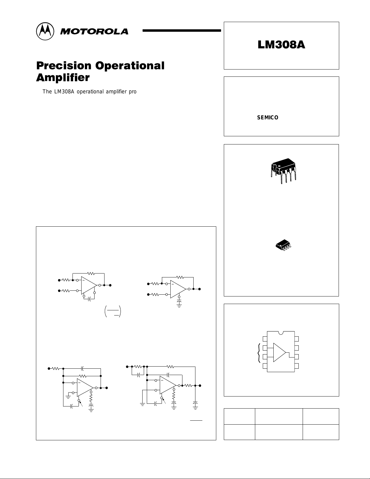
Order this document by LM308A/D
The LM308A operational amplifier provides high input impedance, low
input offset and temperature drift, and low noise. These characteristics are
made possible by use of a special Super Beta processing technology. This
amplifier is particularly useful for applications where high accuracy and low
drift performance are essential. In addition high speed performance may be
improved by employing feedforward compensation techniques to maximize
slew rate without compromising other performance criteria.
The LM308A offers extremely low input offset voltage and drift
specifications allowing usage in even the most critical applications without
external offset nulling.
• Operation from a Wide Range of Power Supply Voltages
• Low Input Bias and Offset Currents
• Low Input Offset Voltage and Guaranteed Offset Voltage Drift
Performance
• High Input Impedance
Frequency Compensation
Standard Compensation
Input
Input
R1
R3
Compen A
Inverting
Noninverting
+
R2
C
f
Cf
Compen B
≥
30
1 +
Output
1
R2
R1
Modified Compensation
Inverting
Noninverting
R1
Input
R3
Input
+
100 pF
R2
Output
Compen B
SUPER GAIN
OPERATIONAL AMPLIFIER
SEMICONDUCTOR
TECHNICAL DATA
8
1
N SUFFIX
PLASTIC PACKAGE
CASE 626
8
1
D SUFFIX
PLASTIC PACKAGE
CASE 751
(SO–8)
PIN CONNECTIONS
Standard Feedforward
Compensation
10 k
Input
500 pF
Compen A
5.0 pF
10
k
+
Compen B
3.0 k
10 pF
Output
Feedforward Compensations for
Decoupling Load Capacitance
RS > 10 k
Input
0.01
MOTOROLA ANALOG IC DEVICE DATA
Compen A Compen B
Inputs
100 k
10 pFC2*
µ
F
+
3.0 k
500 pF
Compen A
500
Compen B
10 pF
*C2 >
5 x 10
R2
Output
C
L
75 pF to
0.01
µ
F
5
pF
Device
LM308AN
LM308AD
Motorola, Inc. 1996 Rev 0
1
–
2
+
3
4
V
EE
(Top View)
ORDERING INFORMATION
Operating
Temperature Range
TA = 0° to +70°C
8
7
6
5
V
Output
NC
CC
Package
Plastic DIP
SO–8
1
Page 2
LM308A
MAXIMUM RATINGS (T
Power Supply Voltage V
Input Voltage (See Note 1) V
Input Differential Current ( See Note 2) I
Output Short Circuit Duration t
Operating Ambient Temperature Range T
Storage Temperature Range T
Junction Temperature T
NOTES: 1. For supply voltages less than ±15 V , the maximum input voltage is equal to the supply
voltage.
2.The inputs are shunted with back–to–back diodes for overvoltage protection. Therefore,
excessive current will flow if a differential input voltage in excess of 1.0 V is applied
between the inputs, unless some limiting resistance is used.
ELECTRICAL CHARACTERISTICS (Unless otherwise noted these specifications apply for supply voltages of +5.0 V ≤ V
and –5.0 V ≥ VEE ≥ –15 V, TA = +25°C.)
Input Offset Voltage V
Input Offset Current I
Input Bias Current I
Input Resistance r
Power Supply Currents ICC, I
(VCC = +15 V, VEE = –15 V)
Large Signal Voltage Gain A
(VCC = +15 V, VEE = –15 V, VO = ±10 V, RL ≥ 10 kΩ)
The following specifications apply over the operating temperature range.
Input Offset Voltage V
Input Offset Current I
Average Temperature Coefficient of Input Offset Voltage ∆VIO/∆T – 1.0 5.0 µV/°C
TA (min) ≤ TA ≤ TA (max)
Average Temperature Coefficient of Input Offset Current ∆IIO/∆T – 2.0 10 pA/°C
Input Bias Current I
Large Signal Voltage Gain A
(VCC +15 V, VEE= –15 V, VO = ±10 V, RL ≥ 10 kΩ)
Input Voltage Range V
(VCC = +15 V, VEE= –15 V)
Common Mode Rejection CMR 96 110 – dB
(RS ≤ 50 kΩ)
Supply Voltage Rejection PSR 96 110 – dB
(RS ≤ 50 kΩ)
Output Voltage Range
(VCC = +15 V, VEE= –15 V, RL = 10 kΩ)
= +25°C, unless otherwise noted.)
A
Rating Symbol Value Unit
CC, VEE
I
ID
SC
A
stg
J
Characteristic
±18 Vdc
±15 V
±10 mA
Indefinite
0 to +70 °C
–65 to +150
+150 °C
Symbol Min Typ Max Unit
IO
IO
IB
i
VOL
IO
IO
IB
VOL
ICR
V
OR
°C
EE
≤ +15 V
CC
– 0.3 0.5 mV
– 0.2 1.0 nA
– 1.5 7.0 nA
10 40 – MΩ
– ±0.3 ±0.8 mA
80 300 – V/mV
– – 0.73 mV
– – 1.5 nA
– – 10 nA
60 – – V/mV
±14 – – V
±13 ±14 – V
2
MOTOROLA ANALOG IC DEVICE DATA
Page 3
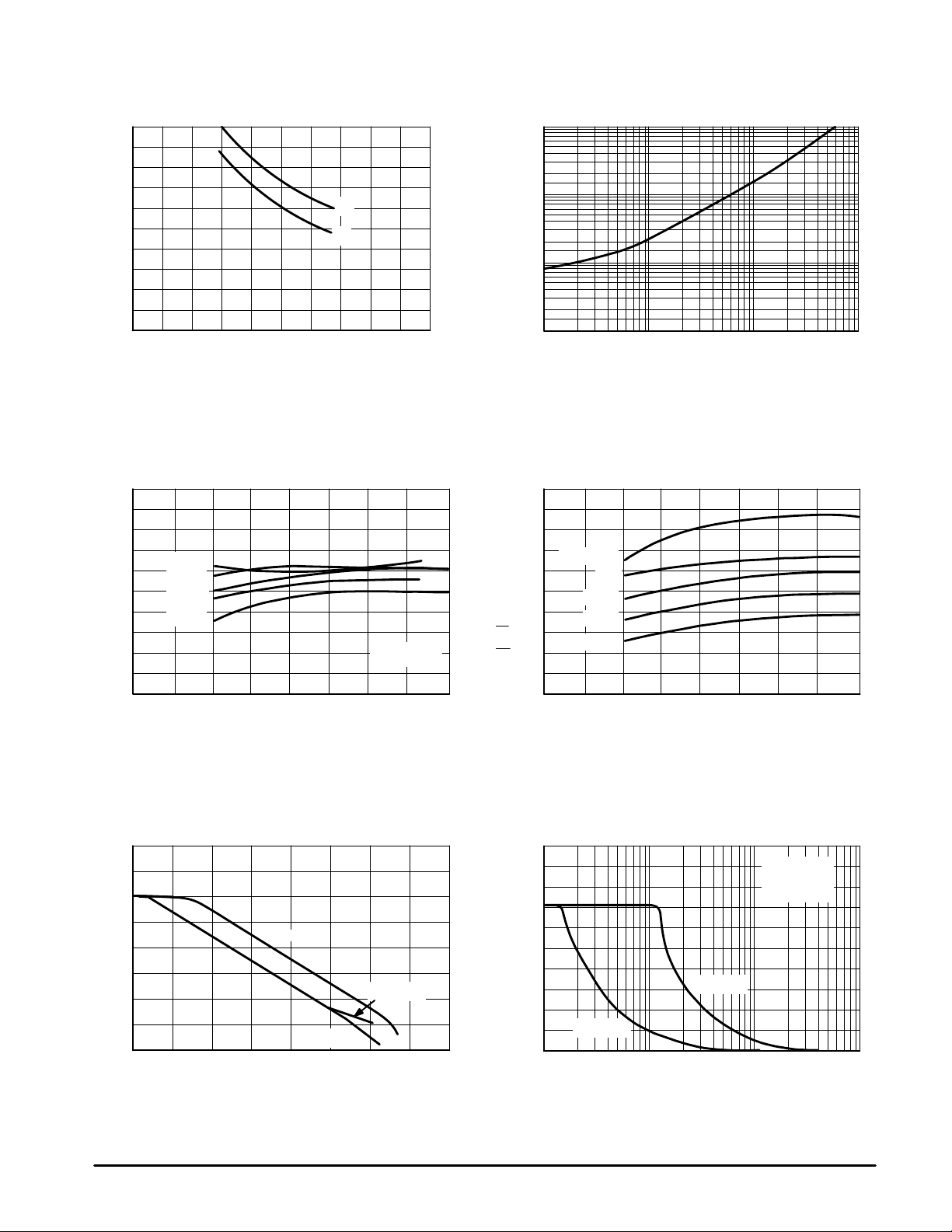
Figure 1. Input Bias and Input Offset Currents
2.0
1.8
1.6
1.4
1.2
1.0
0.8
, INPUT BIAS CURRENT (nA)
0.6
IB
I
0.4
0.2
0
–60 –40 –20 0 20 40 60 80 100 120 140
T, TEMPERATURE (°C) ri, INPUT RESISTANCE (Ω)
I
IO
I
IB
Figure 3. V oltage Gain versus Supply Voltages
130
120
TA = 0°C
110
100
, VOLTAGE GAIN (dB)
VOL
A
90
80
+25°C
–55°C
+70°C
+125°C
CF = 0
f = 100 Hz
0 5.0 10 15 20
VCC = VEE
, SUPPLY VOLTAGES (V)
LM308A
0.25
0.20
0.15
0.10
, INPUT OFFSET CURRENT (nA)
0.05
IO
I
0
Figure 2. Maximum Equivalent Input Offset
V oltage Error versus Input Resistance
100
10
1.0
0.1
EQUIVALENT INPUT OFFSET VOLTAGE (mV)
100 k 1.0 M 10 M 100 M
Figure 4. Power Supply Currents versus
Power Supply Voltages
500
µ
400
TA = –55°C
300
200
, SUPPLY CURRENTS ( A)
EE
I
100
=
CC
I
0
0 5.0 10
0°C
+25°C
+70°C
+125°C
VCC =
VEE
, SUPPLY VOLTAGES (V)
15 20
Figure 5. Open Loop Frequency Response Figure 6. Large Signal Frequency Response
140
120
100
80
60
40
, VOLTAGE GAIN (dB)
20
VOL
A
0
–20
1.0 10 100 1.0 k 10 k 100 k 1.0 M 10 M 100 M
CF = 3.0 pF
CF = 30 pF
CF = 100 pF
f, FREQUENCY (Hz) f, FREQUENCY (Hz)
MOTOROLA ANALOG IC DEVICE DATA
20
)
p–p
16
±
12
8.0
4.0
, OUTPUT VOL TAGE RANGE ( V
OR
V
CF = 30 pF
0
1.0 k 10 k 100 k 1.0 M
CF = 3.0 pF
VCC = +15 V
VEE = –15 V
°
C
TA = +25
3
Page 4

LM308A
SUGGESTED DESIGN APPLICATIONS
INPUT GUARDING
Special care must be taken in the assembly of printed
circuit boards to take full advantage of the low input currents
of the LM308A amplifier. Boards must be thoroughly cleaned
with alcohol and blown dry with compressed air. After
cleaning, the boards should be coated with epoxy or silicone
rubber to prevent contamination.
Figure 7. Fast (1) Summing Amplifier with
Low Input Current
Input
RS
R1
150 k
(1) Power Bandwidth: 250 kHz
Small Signal Bandwidth:
3.5 MHz
Slew Rate: 10 V/
(2) C5 =
6 X 10
R1
0.002µF
LM308A
µ
s
–8
Compen B
300 pF
R2
1 M
(3) In addition to increasing speed,
C5 (2)
R4
0.002
µ
2
3
1.0 M
the LM101A raises high and low
frequency gain, increases output
drive capability and eliminates
thermal feedback.
F
150 pF
1
6
LM101A (3)
or equiv
Output
Even with properly cleaned and coated boards, leakage
currents may cause trouble at +125°C, particularly since the
input pins are adjacent to pins that are at supply potentials.
This leakage can be significantly reduced by using guarding
to lower the voltage difference between the inputs and
adjacent metal runs. The guard, which is a conductive ring
surrounding the inputs, is connected to a low–impedance
point that is at approximately the same voltage as the inputs.
Leakage currents from high voltage pins are then absorbed
by the guard.
Figure 8. Sample and Hold
V
CC
Q1
Q2
F (1)
1.0 M
Output
30 pF
Input
Sample
1.0
µ
(1) Teflon, Polyethylene or Polycarbonate
Dielectric Capacitor
Figure 9. Connection of Input Guards
Inverting Amplifier Follower Noninverting Amplifier
Input
(1) Used to compensate for large source resistances. Note:
4
R1 R2
R3 (1)
C1
Output
R3 (1)
Output
Input
C1
MOTOROLA ANALOG IC DEVICE DATA
R2
R3 (1)
R1
Input
R1 R2
must be an impedance.
R1 +R2
Output
C1
Page 5

15 pF
LM308A
Representative Circuit Schematic
Compensation A Compensation B
7.5 k5.6 k3.5 k
17.4 k
17.4 k
7.5 k
1.0 k
1.4 k
V
CC
Inputs
)
2.0 k
10 k
2.0 k
80 k
1.0 k
7.0 k
V
CC
1.0 k
V
EE
20 k
362 1.2 k 50 k
200
65
150
Output
V
EE
MOTOROLA ANALOG IC DEVICE DATA
5
Page 6

NOTE 2
–T–
SEATING
PLANE
H
OUTLINE DIMENSIONS
58
–B–
14
F
–A–
C
N
D
G
0.13 (0.005) B
K
M
T
LM308A
N SUFFIX
PLASTIC PACKAGE
CASE 626–05
ISSUE K
L
J
M
M
A
M
NOTES:
1. DIMENSION L TO CENTER OF LEAD WHEN
FORMED PARALLEL.
2. PACKAGE CONTOUR OPTIONAL (ROUND OR
SQUARE CORNERS).
3. DIMENSIONING AND TOLERANCING PER ANSI
Y14.5M, 1982.
DIM MIN MAX MIN MAX
A 9.40 10.16 0.370 0.400
B 6.10 6.60 0.240 0.260
C 3.94 4.45 0.155 0.175
D 0.38 0.51 0.015 0.020
F 1.02 1.78 0.040 0.070
G 2.54 BSC 0.100 BSC
H 0.76 1.27 0.030 0.050
J 0.20 0.30 0.008 0.012
K 2.92 3.43 0.1 15 0.135
L 7.62 BSC 0.300 BSC
M ––– 10 ––– 10
N 0.76 1.01 0.030 0.040
INCHESMILLIMETERS
__
A
C
A1
D SUFFIX
PLASTIC PACKAGE
CASE 751–05
(SO–8)
ISSUE R
D
58
0.25MB
E
1
B
e
H
4
M
h
X 45
_
q
C
A
SEATING
PLANE
0.10
L
B
SS
A0.25MCB
NOTES:
1. DIMENSIONING AND TOLERANCING PER ASME
Y14.5M, 1994.
2. DIMENSIONS ARE IN MILLIMETERS.
3. DIMENSION D AND E DO NOT INCLUDE MOLD
PROTRUSION.
4. MAXIMUM MOLD PROTRUSION 0.15 PER SIDE.
5. DIMENSION B DOES NOT INCLUDE MOLD
PROTRUSION. ALLOWABLE DAMBAR
PROTRUSION SHALL BE 0.127 TOTAL IN EXCESS
OF THE B DIMENSION AT MAXIMUM MATERIAL
CONDITION.
MILLIMETERS
DIM MIN MAX
A 1.35 1.75
A1 0.10 0.25
B 0.35 0.49
C 0.18 0.25
D 4.80 5.00
E
3.80 4.00
1.27 BSCe
H 5.80 6.20
h
0.25 0.50
L 0.40 1.25
0 7
q
__
6
MOTOROLA ANALOG IC DEVICE DATA
Page 7

LM308A
Motorola reserves the right to make changes without further notice to any products herein. Motorola makes no warranty , representation or guarantee regarding
the suitability of its products for any particular purpose, nor does Motorola assume any liability arising out of the application or use of any product or circuit, and
specifically disclaims any and all liability, including without limitation consequential or incidental damages. “T ypical” parameters which may be provided in Motorola
data sheets and/or specifications can and do vary in different applications and actual performance may vary over time. All operating parameters, including “Typicals”
must be validated for each customer application by customer’s technical experts. Motorola does not convey any license under its patent rights nor the rights of
others. Motorola products are not designed, intended, or authorized for use as components in systems intended for surgical implant into the body, or other
applications intended to support or sustain life, or for any other application in which the failure of the Motorola product could create a situation where personal injury
or death may occur. Should Buyer purchase or use Motorola products for any such unintended or unauthorized application, Buyer shall indemnify and hold Motorola
and its officers, employees, subsidiaries, affiliates, and distributors harmless against all claims, costs, damages, and expenses, and reasonable attorney fees
arising out of, directly or indirectly, any claim of personal injury or death associated with such unintended or unauthorized use, even if such claim alleges that
Motorola was negligent regarding the design or manufacture of the part. Motorola and are registered trademarks of Motorola, Inc. Motorola, Inc. is an Equal
Opportunity/Affirmative Action Employer.
MOTOROLA ANALOG IC DEVICE DATA
7
Page 8

LM308A
How to reach us:
USA/EUROPE/Locations Not Listed: Motorola Literature Distribution; JAP AN: Nippon Motorola Ltd.; Tatsumi–SPD–JLDC, 6F Seibu–Butsuryu–Center,
P.O. Box 20912; Phoenix, Arizona 85036. 1–800–441–2447 or 602–303–5454 3–14–2 Tatsumi Koto–Ku, Tokyo 135, Japan. 03–81–3521–8315
MFAX: RMF AX0@email.sps.mot.com – TOUCHT ONE 602–244–6609 ASIA/PACIFIC: Motorola Semiconductors H.K. Ltd.; 8B Tai Ping Industrial Park,
INTERNET: http://Design–NET.com 51 Ting Kok Road, Tai Po, N.T., Hong Kong. 852–26629298
8
◊
MOTOROLA ANALOG IC DEVICE DATA
LM308A/D
*LM308A/D*
 Loading...