

Page 1
LM3080
Operational Transconductance Amplifier
LM3080 Operational Transconductance Amplifier
February 1995
General Description
The LM3080 is a programmable transconductance block intended to fulfill a wide variety of variable gain applications.
The LM3080 has differential inputs and high impedance
push-pull outputs. The device has high input impedance and
its transconductance (g
plifier bias current (I
High slew rate together with programmable gain make the
LM3080 an ideal choice for variable gain applications such
as sample and hold, multiplexing, filtering, and multiplying.
The LM3080N and LM3080AN are guaranteed from 0
a
70§C.
) is directly proportional to the am-
m
).
ABC
Cto
§
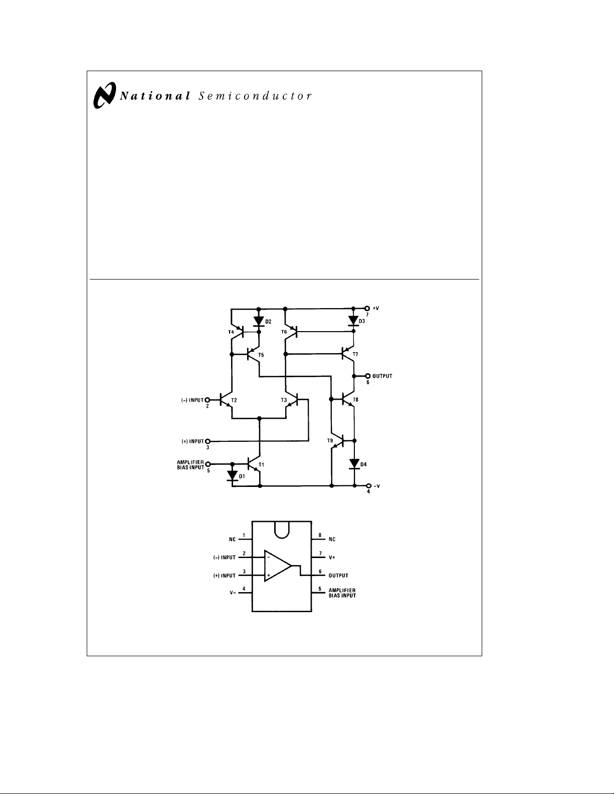
Schematic and Connection Diagrams
Features
Y
Slew rate (unity gain compensated): 50 V/ms
Y
Fully adjustable gain: 0 to g
Y
Extended gmlinearity: 3 decades
Y
Flexible supply voltage range:g2V tog18V
Y
Adjustable power consumption
m
RLlimit
#
TL/H/7148– 1
Dual-In-Line Package
Top View
Order Number LM3080AN, LM3080M or LM3080N
See NS Package Number M08A or N08E
C
1995 National Semiconductor Corporation RRD-B30M115/Printed in U. S. A.
TL/H/7148
TL/H/7148– 2
Page 2
Absolute Maximum Ratings
If Military/Aerospace specified devices are required,
please contact the National Semiconductor Sales
Office/Distributors for availability and specifications.
Supply Voltage (Note 2)
LM3080
LM3080A
g
18V
g
22V
Power Dissipation 250 mW
g
Differential Input Voltage
5V
Amplifier Bias Current (I
DC Input Voltage
)2mA
ABC
a
VStobV
Output Short Circuit Duration Indefinite
Operating Temperature Range
LM3080N or LM3080AN 0
Storage Temperature Range
Ctoa70§C
§
b
65§Ctoa150§C
Lead Temperature (Soldering, 10 sec.) 260§C
S
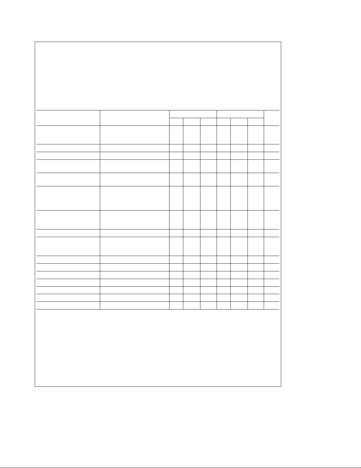
Electrical Characteristics (Note 1)
Parameter Conditions
Input Offset Voltage 0.4 5 0.4 2 mV
Over Specified Temperature Range 6 5 mV
e
I
5 mA 0.3 0.3 2 mV
ABC
Input Offset Voltage Change 5 mAsI
s
500 mA 0.1 0.1 3 mV
ABC
Input Offset Current 0.1 0.6 0.1 0.6 mA
Input Bias Current 0.4 5 0.4 5 mA
Over Specified Temperature Range 1 7 1 8 mA
Forward Transconductance (gm) 6700 9600 13000 7700 9600 12000 mmho
Over Specified Temperature Range 5400 4000 mmho
Peak Output Current R
e
L
e
R
L
e
R
L
Over Specified Temperature Range
e
0, I
0 350 500 650 350 500 650 mA
5 mA5357mA
ABC
0
Peak Output Voltage
Positive R
Negative R
L
L
e %
e %
,5mA
,5mA
s
I
500 mA
ABC
s
s
I
500 mA
ABC
s
Amplifier Supply Current 1.1 1.1 mA
Input Offset Voltage Sensitivity
Positive DV
Negative DV
OFFSET
OFFSET
/DV
/DV
a
b
Common Mode Rejection Ratio 80 110 80 110 dB
Common Mode Range
Input Resistance 10 26 10 26 kX
Magnitude of Leakage Current I
Differential Input Current I
e
0 0.2 100 0.2 5 nA
ABC
ABC
e
0, Input
e
g
4V 0.02 100 0.02 5 nA
Open Loop Bandwidth 2 2 MHz
Slew Rate Unity Gain Compensated 50 50 V/ms
Note 1: These specifications apply for V
Note 2: Selection to supply voltage above
e
g
15V and T
S
g
22V, contact the factory.
e
25§C, amplifier bias current (I
A
LM3080 LM3080A
Units
Min Typ Max Min Typ Max
300 300 mA
a12a
b12b
14.2
14.4
a12a
b12b
14.2 V
14.4 V
20 150 20 150 mV/V
20 150 20 150 mV/V
g
12g14
)e500 mA, unless otherwise specified.
ABC
g
12g14 V
2
Page 3

Typical Performance Characteristics
Input Offset Voltage Input Offset Current Input Bias Current
Peak Output Current Common Mode Range
Total Power Dissipation Leakage Current Input Leakage
Transconductance Input Resistance Amplifier Bias Current
Peak Output Voltage and
Amplifier Supply Current
Amplifier Bias Voltage vs
TL/H/7148– 3
3
Page 4

Typical Performance Characteristics (Continued)
Input and Output Capacitance
Leakage Current Test Circuit
Differential Input Current Test Circuit
TL/H/7148– 4
TL/H/7148– 6
Output Resistance
TL/H/7148– 5
Unity Gain Follower
TL/H/7148– 7
TL/H/7148– 8
4
Page 5

Physical Dimensions inches (millimeters)
Molded Package SO (M)
Order Number LM3080M
NS Package Number M08A
5
Page 6

Physical Dimensions inches (millimeters) (Continued)
Molded Dual-In-Line Package (N)
Order Number LM3080AN or LM3080N
LM3080 Operational Transconductance Amplifier
NS Package Number N08E
LIFE SUPPORT POLICY
NATIONAL’S PRODUCTS ARE NOT AUTHORIZED FOR USE AS CRITICAL COMPONENTS IN LIFE SUPPORT
DEVICES OR SYSTEMS WITHOUT THE EXPRESS WRITTEN APPROVAL OF THE PRESIDENT OF NATIONAL
SEMICONDUCTOR CORPORATION. As used herein:
1. Life support devices or systems are devices or 2. A critical component is any component of a life
systems which, (a) are intended for surgical implant support device or system whose failure to perform can
into the body, or (b) support or sustain life, and whose be reasonably expected to cause the failure of the life
failure to perform, when properly used in accordance support device or system, or to affect its safety or
with instructions for use provided in the labeling, can effectiveness.
be reasonably expected to result in a significant injury
to the user.
National Semiconductor National Semiconductor National Semiconductor National Semiconductor
Corporation Europe Hong Kong Ltd. Japan Ltd.
1111 West Bardin Road Fax: (
Arlington, TX 76017 Email: cnjwge@tevm2.nsc.com Ocean Centre, 5 Canton Rd. Fax: 81-043-299-2408
Tel: 1(800) 272-9959 Deutsch Tel: (
Fax: 1(800) 737-7018 English Tel: (
National does not assume any responsibility for use of any circuitry described, no circuit patent licenses are implied and National reserves the right at any time without notice to change said circuitry and specifications.
Fran3ais Tel: (
Italiano Tel: (
a
49) 0-180-530 85 86 13th Floor, Straight Block, Tel: 81-043-299-2309
a
49) 0-180-530 85 85 Tsimshatsui, Kowloon
a
49) 0-180-532 78 32 Hong Kong
a
49) 0-180-532 93 58 Tel: (852) 2737-1600
a
49) 0-180-534 16 80 Fax: (852) 2736-9960
 Loading...