

Page 1
LM3046
Transistor Array
General Description
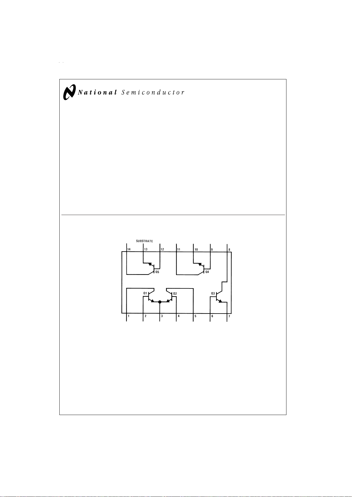
The LM3046 consists of five general purpose silicon NPN
transistors on a common monolithic substrate. Two of the
transistors are internally connected to form a
differentially-connected pair. The transistors are well suited
to a wide variety of applications in low power system in the
DC through VHF range. They maybe used as discrete transistors in conventional circuits however, in addition, they provide the very significant inherent integrated circuit advantages of close electrical and thermal matching. The LM3046
is supplied in a 14-lead molded dual-in-line package.
Features
n Two matched pairs of transistors
V
BE
matched±5mV
Input offset current 2 µA max at I
C
=
1mA
n Five general purpose monolithic transistors
n Operation from DC to 120 MHz
n Wide operating current range
n Low noise figure: 3.2 dB typ at 1 kHz
Applications
n General use in all types of signal processing systems
operating anywhere in the frequency range from DC to
VHF
n Custom designed differential amplifiers
n Temperature compensated amplifiers
Schematic and Connection Diagram
Small Outline Package
DS007950-1
Top View
Order Number LM3046M
See NS Package Number M14A
July 1999
LM3046 Transistor Array
© 1999 National Semiconductor Corporation DS007950 www.national.com
Page 2
Absolute Maximum Ratings (Note 1)
If Military/Aerospace specified devices are required, please contact the National Semiconductor Sales Office/
Distributors for availability and specifications. (T
A
=
25˚C)
LM3046
Each Total Units
Transistor Package
Power Dissipation:
T
A
=
25˚C 300 750 mW
T
A
=
25˚C to 55˚C 300 750 mW
T
A
>
55˚C Derate at 6.67 mW/˚C
T
A
=
25˚C to 75˚C mW
T
A
>
75˚C mW/˚C
Collector to Emitter Voltage, V
CEO
15 V
Collector to Base Voltage, V
CBO
20 V
Collector to Substrate Voltage, V
CIO
(Note 2) 20 V
Emitter to Base Voltage, V
EBO
5V
Collector Current, I
C
50 mA
Operating Temperature Range −40˚C to +85˚C
Storage Temperature Range −65˚C to +85˚C
Soldering Information
Dual-In-Line Package Soldering (10 Sec.) 260˚C
Small Outline Package
Vapor Phase (60 Seconds) 215˚C
Infrared (15 Seconds) 220˚C
SeeAN-450 “Surface Mounting Methods and Their Effect on Product Reliability” for other methods of soldering surface mount devices.
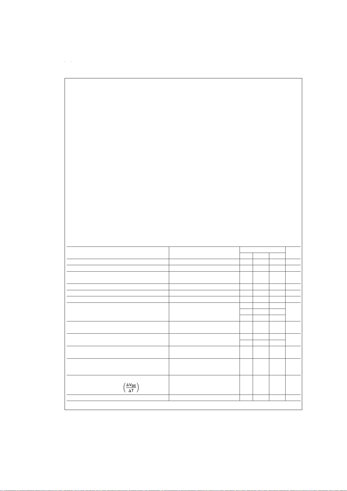
Electrical Characteristics
(T
A
=
25˚C unless otherwise specified)
Parameter Conditions
Limits
Units
Min Typ Max
Collector to Base Breakdown Voltage (V
(BR)CBO
)I
C
=
10 µA, I
E
=
02060V
Collector to Emitter Breakdown Voltage (V
(BR)CEO
)I
C
=
1 mA, I
B
=
01524V
Collector to Substrate Breakdown I
C
=
10 µA, I
CI
=
02060V
Voltage (V
(BR)CIO
)
Emitter to Base Breakdown Voltage (V
(BR)EBO
)I
E
10 µA, I
C
=
057V
Collector Cutoff Current (I
CBO
)V
CB
=
10V, I
E
=
0 0.002 40 nA
Collector Cutoff Current (I
CEO
)V
CE
=
10V, I
B
=
0 0.5 µA
Static Forward Current Transfer V
CE
=
3V I
C
=
10 mA 100
Ratio (Static Beta) (h
FE
)I
C
=
1 mA 40 100
I
C
=
10 µA 54
Input Offset Current for Matched V
CE
=
3V, I
C
=
1 mA 0.3 2 µA
Pair Q
1
and Q2|IO1−I
IO2
|
Base to Emitter Voltage (V
BE
)V
CE
=
3V I
E
=
1 mA 0.715 V
I
E
=
10 mA 0.800
Magnitude of Input Offset Voltage for V
CE
=
3V, I
C
=
1 mA 0.45 5 mV
Differential Pair |V
BE1−VBE2
|
Magnitude of Input Offset Voltage for Isolated
Transistors |V
BE3−VBE4
|, |V
BE4−VBE5
|,
|V
BE5−VBE3
|
V
CE
=
3V, I
C
=
1 mA 0.45 5 mV
Temperature Coefficient of Base to
Emitter Voltage
V
CE
=
3V, I
C
=
1 mA −1.9 mV/˚C
Collector to Emitter Saturation Voltage (V
CE(SAT)
)I
B
=
1 mA, I
C
=
10 mA 0.23 V
www.national.com 2
Page 3

Electrical Characteristics (Continued)
(T
A
=
25˚C unless otherwise specified)
Parameter Conditions
Limits
Units
Min Typ Max
Temperature Coefficient of
Input Offset Voltage
V
CE
=
3V, I
C
=
1 mA 1.1 µV/˚C
Note 1: “Absolute Maximum Ratings” indicate limits beyond which damage to the device may occur. Operating Ratings indicate conditions for which the device is
functional, but do not guarantee specific performance limits.
Note 2: The collector of each transistor is isolated from the substrate by an integral diode. The substrate (terminal 13) must be connected to the most negative point
in the external circuit to maintain isolation between transistors and to provide for normal transistor action.
Electrical Characteristics
Parameter Conditions Min Typ Max Units
Low Frequency Noise Figure (NF) f=1 kHz, V
CE
=
3V, 3.25 dB
I
C
=
100 µA, R
S
=
1kΩ
LOW FREQUENCY, SMALL SIGNAL EQUIVALENT CIRCUIT CHARACTERISTICS
Forward Current Transfer Ratio (h
fe
)f
=
1 kHz, V
CE
=
3V, 110
I
C
=
1mA
Short Circuit Input Impednace (h
ie
) 3.5 kΩ
Open Circuit Output Impedance (h
oe
) 15.6 µmho
Open Circuit Reverse Voltage Transfer Ratio
(h
re
)
1.8x10
−4
ADMITTANCE CHARACTERISTICS
Forward Transfer Admittance (Y
fe
)f
=
1 MHz, V
CE
=
3V, 31 − j 1.5
Input Admittance (Y
ie
)I
C
=
1 mA 0.3+J 0.04
Output Admittance (Y
oe
) 0.001+j 0.03
Reverse Transfer Admittance (Y
re
) See Curve
Gain Bandwidth Product (f
T
)V
CE
=
3V, I
C
=
3 mA 300 550
Emitter to Base Capacitance (C
EB
)V
EB
=
3V, I
E
=
0 0.6 pF
Collector to Base Capacitance (C
CB
)V
CB
=
3V, I
C
=
0 0.58 pF
Collector to Substrate Capacitance (C
CI
)V
CS
=
3V, I
C
=
0 2.8 pF
Typical Performance Characteristics
Typical Collector To Base
Cutoff Current vs Ambient
Temperature for Each
Transistor
DS007950-8
Typical Collector To Emitter
Cutoff Current vs Ambient
Temperature for Each
Transistor
DS007950-9
Typical Static Forward
Current-Transfer Ratio and
Beta Ratio for Transistors Q
1
and Q2vs Emitter Current
DS007950-10
www.national.com3
Page 4

Typical Performance Characteristics (Continued)
Typical Input Offset Current
for Matched Transistor Pair
Q
1Q2
vs Collector Current
DS007950-11
Typical Static Base To Emitter
Voltage Characteristic and Input
Offset Voltage for Differential
Pair and Paired Isolated
Transistors vs Emitter Current
DS007950-12
Typical Base To Emitter
Voltage Characteristic for
Each Transistor vs Ambient
Temperature
DS007950-13
Typical Input Offset Voltage
Characteristics for Differential
Pair and Paired Isolated
Transistors vs Ambient
Temperature
DS007950-14
Typical Noise Figure vs
Collector Current
DS007950-15
Typical Noise Figure vs
Collector Current
DS007950-16
Typical Noise Figure vs
Collector Current
DS007950-17
Typical Normalized Forward
Current Transfer Ratio, Short
Circuit Input Impedance,
Open Circuit Output Impedance,
and Open Circuit Reverse
Voltage Transfer Ratio vs
Collector Current
DS007950-18
Typical Forward Transfer
Admittance vs Frequency
DS007950-19
www.national.com 4
Page 5

Typical Performance Characteristics (Continued)
Typical Input Admittance
vs Frequency
DS007950-20
Typical Output Admittance
vs Frequency
DS007950-21
Typical Reverse Transfer
Admittance vs Frequency
DS007950-22
Typical Gain-Bandwidth
Product vs Collector Current
DS007950-23
www.national.com5
Page 6

Physical Dimensions inches (millimeters) unless otherwise noted
LIFE SUPPORT POLICY
NATIONAL’S PRODUCTS ARE NOT AUTHORIZED FOR USE AS CRITICAL COMPONENTS IN LIFE SUPPORT
DEVICES OR SYSTEMS WITHOUT THE EXPRESS WRITTEN APPROVAL OF THE PRESIDENT AND GENERAL
COUNSEL OF NATIONAL SEMICONDUCTOR CORPORATION. As used herein:
1. Life support devices or systems are devices or
systems which, (a) are intended for surgical implant
into the body, or (b) support or sustain life, and
whose failure to perform when properly used in
accordance with instructions for use provided in the
labeling, can be reasonably expected to result in a
significant injury to the user.
2. A critical component is any component of a life
support device or system whose failure to perform
can be reasonably expected to cause the failure of
the life support device or system, or to affect its
safety or effectiveness.
National Semiconductor
Corporation
Americas
Tel: 1-800-272-9959
Fax: 1-800-737-7018
Email: support@nsc.com
National Semiconductor
Europe
Fax: +49 (0) 1 80-530 85 86
Email: europe.support@nsc.com
Deutsch Tel: +49 (0) 1 80-530 85 85
English Tel: +49 (0) 1 80-532 78 32
Français Tel: +49 (0) 1 80-532 93 58
Italiano Tel: +49 (0) 1 80-534 16 80
National Semiconductor
Asia Pacific Customer
Response Group
Tel: 65-2544466
Fax: 65-2504466
Email: sea.support@nsc.com
National Semiconductor
Japan Ltd.
Tel: 81-3-5639-7560
Fax: 81-3-5639-7507
www.national.com
Molded Small Outline Package (M)
Order Number LM3046M
NS Package Number M14A
LM3046 Transistor Array
National does not assume any responsibility for use of any circuitry described, no circuit patent licenses are implied and National reserves the right at any time without notice to change said circuitry and specifications.
 Loading...