

Page 1
LM101A/LM201A/LM301A Operational Amplifiers
General Description
The LM101A series are general purpose operational amplifiers which feature improved performance over industry standards like the LM709. Advanced processing techniques
make possible an order of magnitude reduction in input currents, and a redesign of the biasing circuitry reduces the
temperature drift of input current. Improved specifications
include:
Y
Offset voltage 3 mV maximum over
temperature (LM101A/LM201A)
Y
Input current 100 nA maximum over
temperature (LM101A/LM201A)
Y
Offset current 20 nA maximum over
temperature (LM101A/LM201A)
Y
Guaranteed drift characteristics
Y
Offsets guaranteed over entire common mode and supply voltage ranges
Y
Slew rate of 10V/ms as a summing amplifier
This amplifier offers many features which make its application nearly foolproof: overload protection on the input and
output, no latch-up when the common mode range is ex-
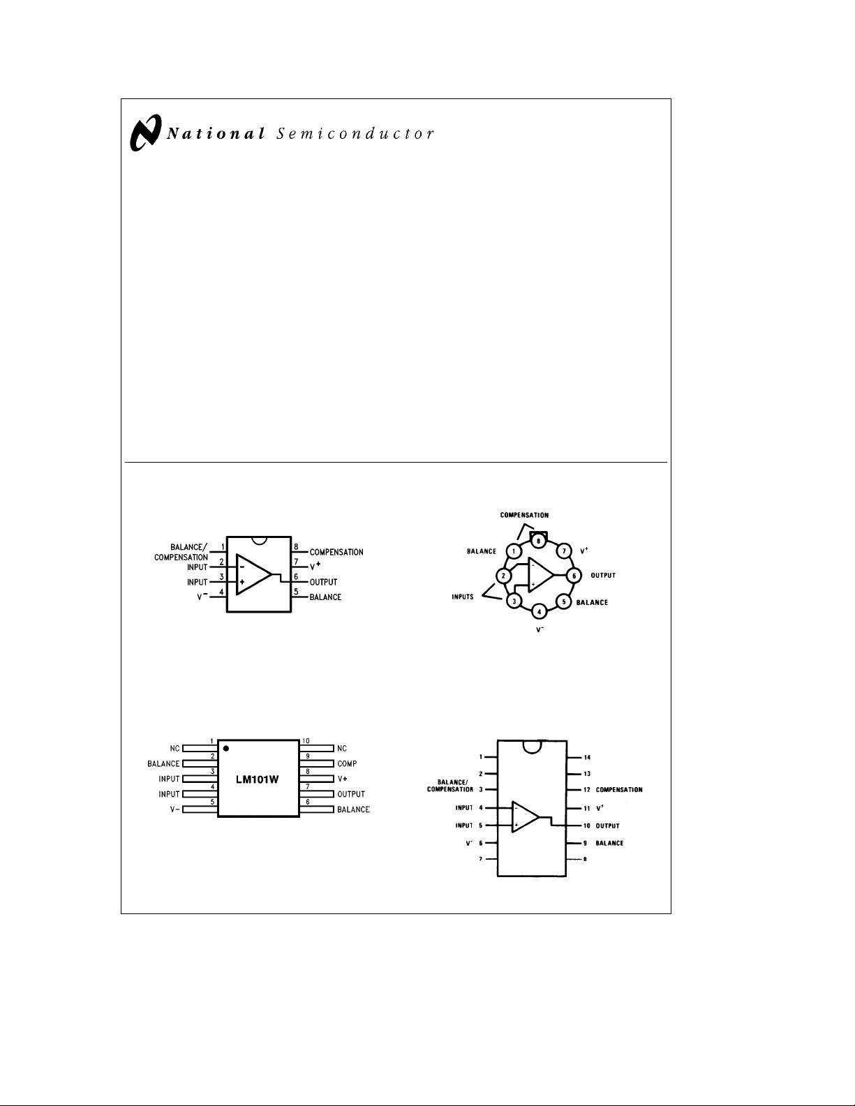
Connection Diagrams (Top View)
ceeded, and freedom from oscillations and compensation
with a single 30 pF capacitor. It has advantages over internally compensated amplifiers in that the frequency compensation can be tailored to the particular application. For example, in low frequency circuits it can be overcompensated
for increased stability margin. Or the compensation can be
optimized to give more than a factor of ten improvement in
high frequency performance for most applications.
In addition, the device provides better accuracy and lower
noise in high impedance circuitry. The low input currents
also make it particularly well suited for long interval integrators or timers, sample and hold circuits and low frequency
waveform generators. Further, replacing circuits where
matched transistor pairs buffer the inputs of conventional IC
op amps, it can give lower offset voltage and a drift at a
lower cost.
The LM101A is guaranteed over a temperature range of
b
55§Ctoa125§C, the LM201A fromb25§Ctoa85§C,
and the LM301A from 0
Ctoa70§C.
§
Metal Can Package
LM101A/LM201A/LM301A Operational Amplifiers
December 1994
Dual-In-Line Package
Order Number LM101AJ, LM101J/883*,
LM201AN or LM301AN
See NS Package Number J08A or N08A
TL/H/7752– 4
TL/H/7752– 2
Note: Pin 4 connected to case.
Order Number LM101AH,
LM101AH/883*, LM201AH or LM301AH
See NS Package Number H08C
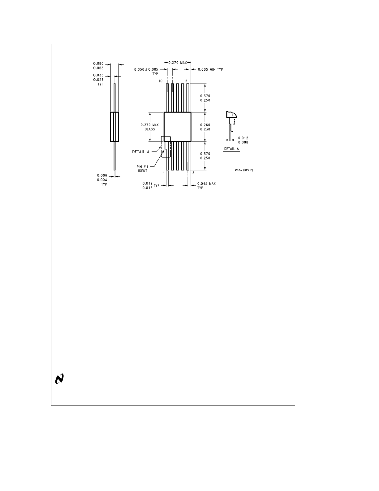
Ceramic Flatpack Package
TL/H/7752– 4
Dual-In-Line Package
Order Number LM101AW/883 or LM101W/883
See NS Package Number W10A
Order Number LM101AJ-14/883*
TL/H/7752– 3
*Available per JM38510/10103.
C
1995 National Semiconductor Corporation RRD-B30M115/Printed in U. S. A.
TL/H/7752
See NS Package Number J14A
Page 2
Absolute Maximum Ratings
If Military/Aerospace specified devices are required, please contact the National Semiconductor Sales Office/
Distributors for availability and specifications.
LM101A/LM201A LM301A
Supply Voltage
Differential Input Voltage
Input Voltage (Note 1)
Output Short Circuit Duration (Note 2) Continuous Continuous
Operating Ambient Temp. Range
T
Max
J
H-Package 150
b
b
N-Package 150
J-Package 150
Power Dissipation at T
H-Package (Still Air) 500 mW 300 mW
e
25§C
A
g
22V
g
30V
g
15V
55§Ctoa125§C (LM101A) 0§Ctoa70§C
25§Ctoa85§C (LM201A)
C 100§C
§
C 100§C
§
C 100§C
§
(400 LF/Min Air Flow) 1200 mW 700 mW
N-Package 900 mW 500 mW
J-Package 1000 mW 650 mW
Thermal Resistance (Typical) i
H-Package (Still Air) 165§C/W 165§C/W
(400 LF/Min Air Flow) 67
N Package 135
J-Package 110
(Typical) i
jC
H-Package 25§C/W 25§C/W
Storage Temperature Range
jA
C/W 67§C/W
§
C/W 135§C/W
§
C/W 110§CmW
§
b
65§Ctoa150§C
Lead Temperature (Soldering, 10 sec.)
Metal Can or Ceramic 300
Plastic 260
ESD Tolerance (Note 5) 2000V 2000V
C 300§C
§
C 260§C
§
g
18V
g
30V
g
15V
b
65§Ctoa150§C
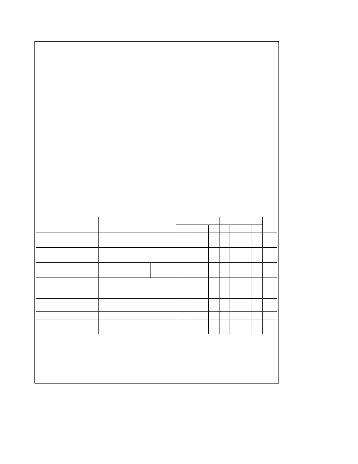
Electrical Characteristics (Note 3) T
Parameter Conditions
e
T
A
J
LM101A/LM201A LM301A
Units
Min Typ Max Min Typ Max
Input Offset Voltage T
Input Offset Current T
Input Bias Current T
Input Resistance T
Supply Current T
Large Signal Voltage Gain T
Input Offset Voltage R
Average Temperature Coefficient R
of Input Offset Voltage
e
A
e
A
e
A
e
A
e
A
e
A
V
OUT
s
S
s
S
s
25§C, R
50 kX 0.7 2.0 2.0 7.5 mV
S
25§C 1.5 10 3.0 50 nA
25§C 30 75 70 250 nA
25§C 1.5 4.0 0.5 2.0 MX
e
25§CV
e
g
10V, R
g
15V
S
t
2kX
L
25§C, V
e
g
20V 1.8 3.0 mA
S
e
g
V
15V 1.8 3.0 mA
S
50 160 25 160 V/mV
50 kX 3.0 10 mV
50 kX
3.0 15 6.0 30 mV/
Input Offset Current 20 70 nA
Average Temperature Coefficient 25§CsT
of Input Offset Current T
MIN
s
T
A
s
MAX
s
T
25§C
A
0.01 0.1 0.01 0.3 nA/§C
0.02 0.2 0.02 0.6 nA/§C
C
§
2
Page 3
Electrical Characteristics (Note 3) T
Parameter Conditions
e
TJ(Continued)
A
LM101A/LM201A LM301A
Units
Min Typ Max Min Typ Max
Input Bias Current 0.1 0.3 mA
Supply Current T
Large Signal Voltage Gain V
Output Voltage Swing V
Input Voltage Range V
Common-Mode Rejection Ratio R
Supply Voltage Rejection Ratio R
Note 1: For supply voltages less thang15V, the absolute maximum input voltage is equal to the supply voltage.
Note 2: Continuous short circuit is allowed for case temperatures to 125
respectively for LM301A.
Note 3: Unless otherwise specified, these specifications apply for C1
b
and
Note 4: Refer to RETS101AX for LM101A military specifications and RETS101X for LM101 military specifications.
Note 5: Human body model, 100 pF discharged through 1.5 kX.
25§CsT
s
a
85§C (LM201A),g5VsV
A
e
T
A
e
g
S
t
R
2k
L
e
g
S
e
g
S
e
g
V
S
s
50 kX 80 96 70 90 dB
S
s
50 kX 80 96 70 96 dB
S
e
g
MAX,VS
15V, V
20V 1.2 2.5 mA
e
g
10V
OUT
15V R
20V
15V
e
s
g
15V and 0§CsT
S
30 pF,g5VsV
25 15 V/mV
e
10 kXg12
L
e
R
2kXg10
L
C and ambient temperatures to 75§C for LM101A/LM201A, and 70§C and 55§C
§
s
g
S
s
a
70§C (LM301A).
A
g
14
g
13
g
15 V
a
15,b13
20V andb55§CsT
g
12
g
10
g
12a15,b13 V
s
a
125§C (LM101A),g5VsV
A
g
14 V
g
13 V
S
s
g
20V
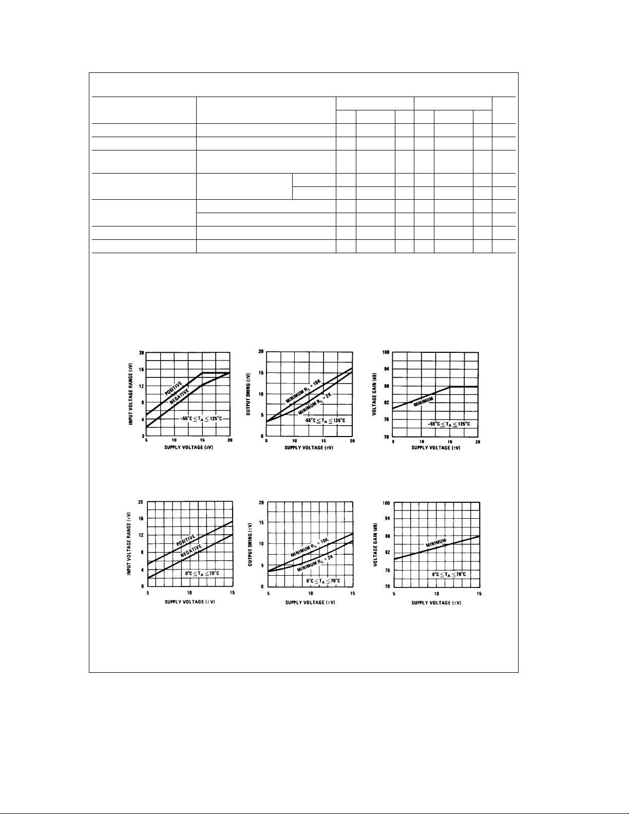
Guaranteed Performance Characteristics LM101A/LM201A
Input Voltage Range Output Swing Voltage Gain
Guaranteed Performance Characteristics LM301A
Input Voltage Range Output Swing Voltage Gain
3
TL/H/7752– 5
TL/H/7752– 6
Page 4
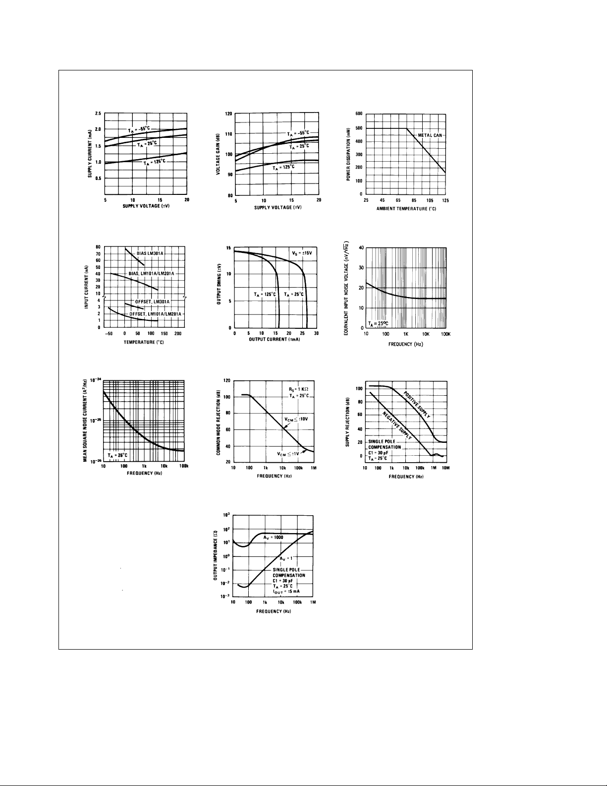
Typical Performance Characteristics
Supply Current Voltage Gain Maximum Power Dissipation
Input Current,
LM101A/LM201A/LM301A
Current Limiting Input Noise Voltage
Input Noise Current Common Mode Rejection Power Supply Rejection
Closed Loop Output
Impedance
TL/H/7752– 7
4
Page 5
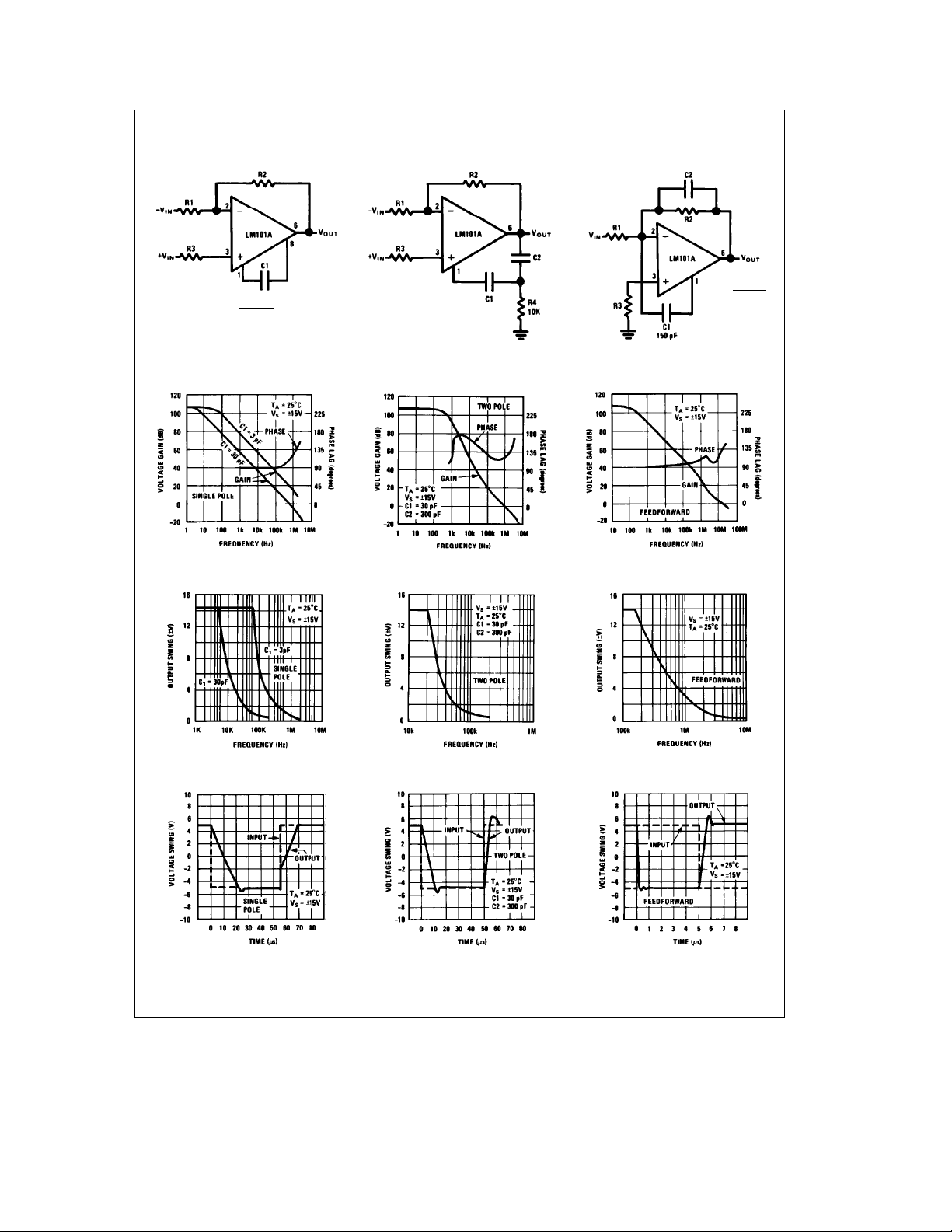
Typical Performance Characteristics for Various Compensation Circuits**
Single Pole Compensation
Two Pole Compensation
Feedforward Compensation
R1 C
S
t
C1
R1aR2
e
C
30 pF
S
Open Loop Frequency
Response
Large Signal Frequency
Response
TL/H/7752– 8
TL/H/7752– 9
R1 C
S
t
C1
R1aR2
e
C
30 pF
S
e
C2
10 C1
TL/H/7752– 12
Open Loop Frequency
Response
Large Signal Frequency
TL/H/7752– 13
Response
C2
f
o
TL/H/7752– 16
Open Loop Frequency
Response
Large Signal Frequency
TL/H/7752– 17
Response
e
e
1
2q foR2
3 MHz
Voltage Follower Pulse
TL/H/7752– 10
Response
TL/H/7752– 11
**Pin connections shown are for 8-pin packages.
Voltage Follower Pulse
TL/H/7752– 14
Response
TL/H/7752– 15
5
TL/H/7752– 18
Inverter Pulse Response
TL/H/7752– 19
Page 6
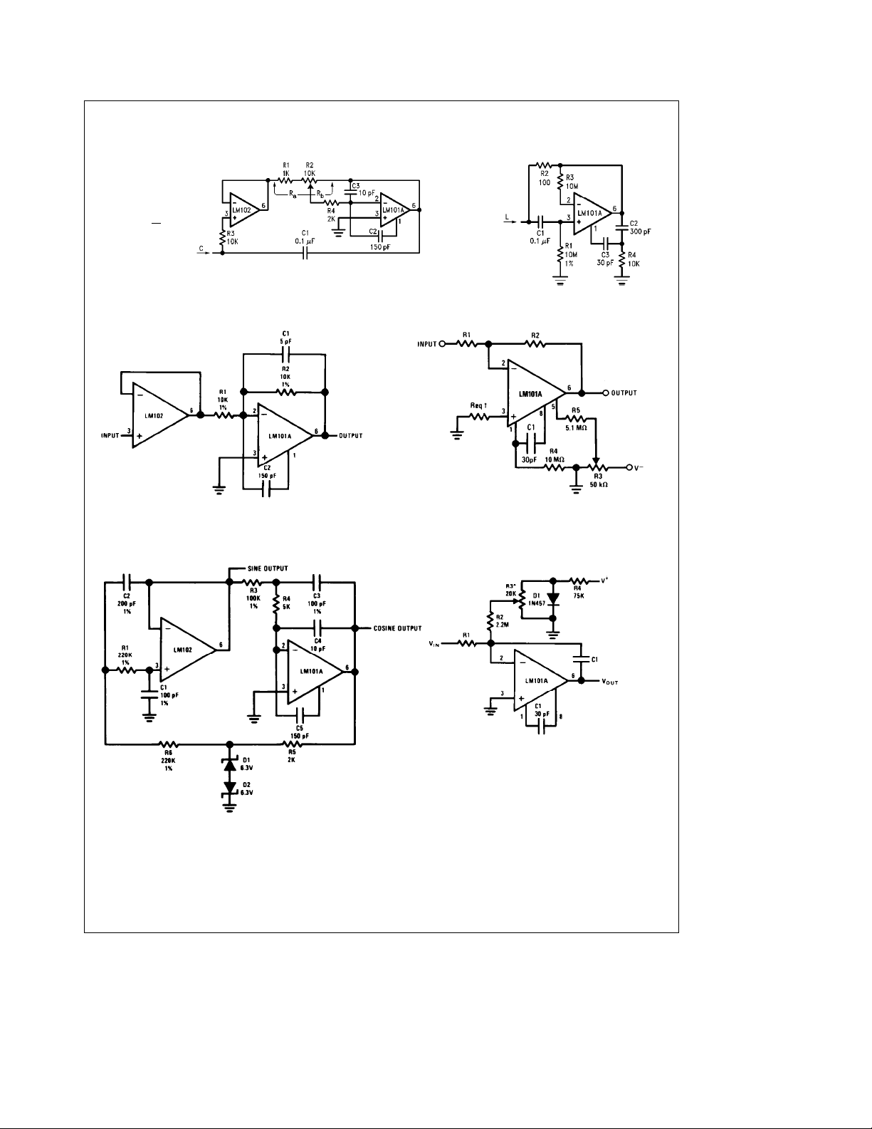
Typical Applications**
Variable Capacitance Multiplier
R
b
a
Ce1
C1
R
a
Fast Inverting Amplifier
with High Input Impedance
TL/H/7752– 22
TL/H/7752– 20
²
May be zero or equal
to parallel combination of R1 and R2 for
minimum offset.
Simulated Inductor
LjR1 R2 C1
e
R
R2
S
e
R
R1
P
Inverting Amplifier
with Balancing Circuit
TL/H/7752– 21
TL/H/7752– 23
Sine Wave Oscillator
**Pin connections shown are for 8-pin packages.
f
o
e
10 kHz
TL/H/7752– 24
6
Integrator with Bias Current
Compensation
*Adjust for zero integrator drift. Current drift typically
C overb55§Ctoa125§C temperature range.
0.1 nA/
§
TL/H/7752– 25
Page 7
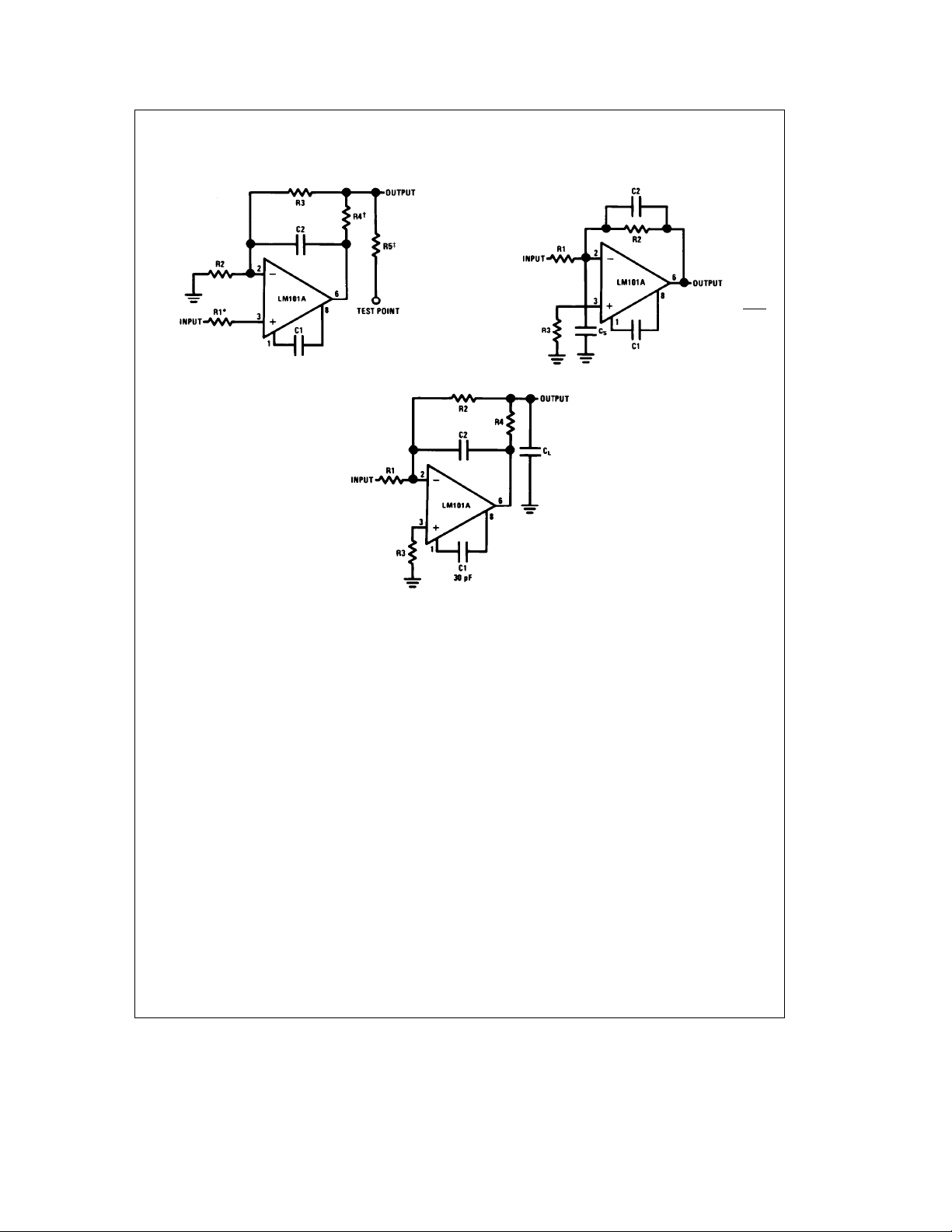
Application Hints**
Protecting Against Gross
Fault Conditions
*Protects input
²
Protects output
³
Protects outputÐnot needed when R4 is used.
Compensating for Stray Input Capacitances
TL/H/7752– 26
Isolating Large Capacitive Loads
or Large Feedback Resistor
R1 C
e
C2
R2
TL/H/7752– 27
S
Although the LM101A is designed for trouble free operation,
experience has indicated that it is wise to observe certain
precautions given below to protect the devices from abnormal operating conditions. It might be pointed out that the
advice given here is applicable to practically any IC op amp,
although the exact reason why may differ with different devices.
When driving either input from a low-impedance source, a
limiting resistor should be placed in series with the input
lead to limit the peak instantaneous output current of the
source to something less than 100 mA. This is especially
important when the inputs go outside a piece of equipment
where they could accidentally be connected to high voltage
sources. Large capacitors on the input (greater than 0.1 mF)
should be treated as a low source impedance and isolated
with a resistor. Low impedance sources do not cause a
problem unless their output voltage exceeds the supply voltage. However, the supplies go to zero when they are turned
off, so the isolation is usually needed.
The output circuitry is protected against damage from shorts
to ground. However, when the amplifier output is connected
to a test point, it should be isolated by a limiting resistor, as
test points frequently get shorted to bad places. Further,
when the amplifer drives a load external to the equipment, it
is also advisable to use some sort of limiting resistance to
preclude mishaps.
**Pin connections shown are for 8-pin packages.
TL/H/7752– 28
Precautions should be taken to insure that the power supplies for the integrated circuit never become reversedÐ
even under transient conditions. With reverse voltages
greater than 1V, the IC will conduct excessive current, fusing internal aluminum interconnects. If there is a possibility
of this happening, clamp diodes with a high peak current
rating should be installed on the supply lines. Reversal of
the voltage between V
a
and Vbwill always cause a problem, although reversals with respect to ground may also
give difficulties in many circuits.
The minimum values given for the frequency compensation
capacitor are stable only for source resistances less than
10 kX, stray capacitances on the summing junction less
than 5 pF and capacitive loads smaller than 100 pF. If any
of these conditions are not met, it becomes necessary to
overcompensate the amplifier with a larger compensation
capacitor. Alternately, lead capacitors can be used in the
feedback network to negate the effect of stray capacitance
and large feedback resistors or an RC network can be added to isolate capacitive loads.
Although the LM101A is relatively unaffected by supply bypassing, this cannot be ignored altogether. Generally it is
necessary to bypass the supplies to ground at least once on
every circuit card, and more bypass points may be required
if more than five amplifiers are used. When feed-forward
compensation is employed, however, it is advisable to bypass the supply leads of each amplifier with low inductance
capacitors because of the higher frequencies involved.
7
Page 8
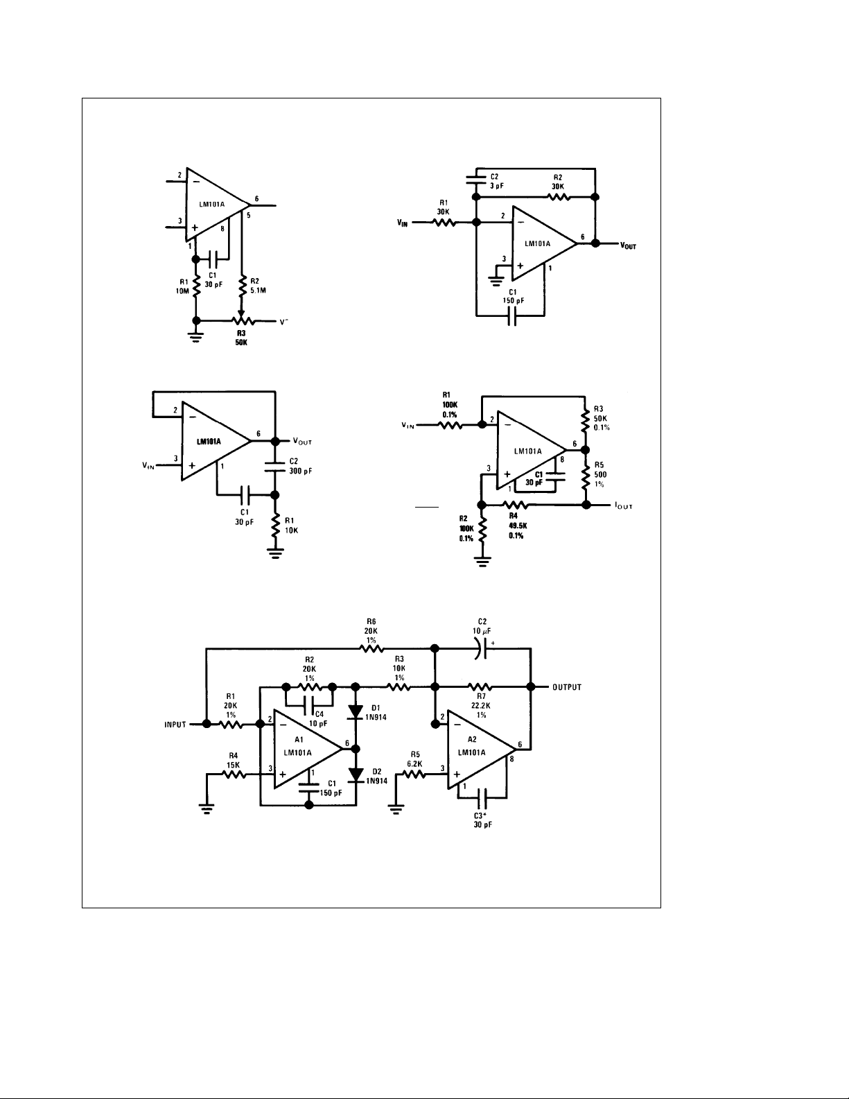
Typical Applications** (Continued)
Standard Compensation and
Offset Balancing Circuit
Fast Voltage Follower
TL/H/7752– 29
Fast Summing Amplifier
Power Bandwidth: 250 kHz
Small Signal Bandwiidth: 3.5 MHz
Slew Rate: 10V/ms
Bilateral Current Source
TL/H/7752– 30
Power Bandwidth: 15 kHz
Slew Rate: 1V/ms
**Pin connections shown are for 8-pin packages.
I
OUT
R3
R1
TL/H/7752– 31
Fast AC/DC Converter*
R3 V
e
R1 R5
eR4a
e
R2
IN
R5
TL/H/7752– 32
*Feedforward compensation
can be used to make a fast full
wave rectifier without a filter.
TL/H/7752– 33
8
Page 9
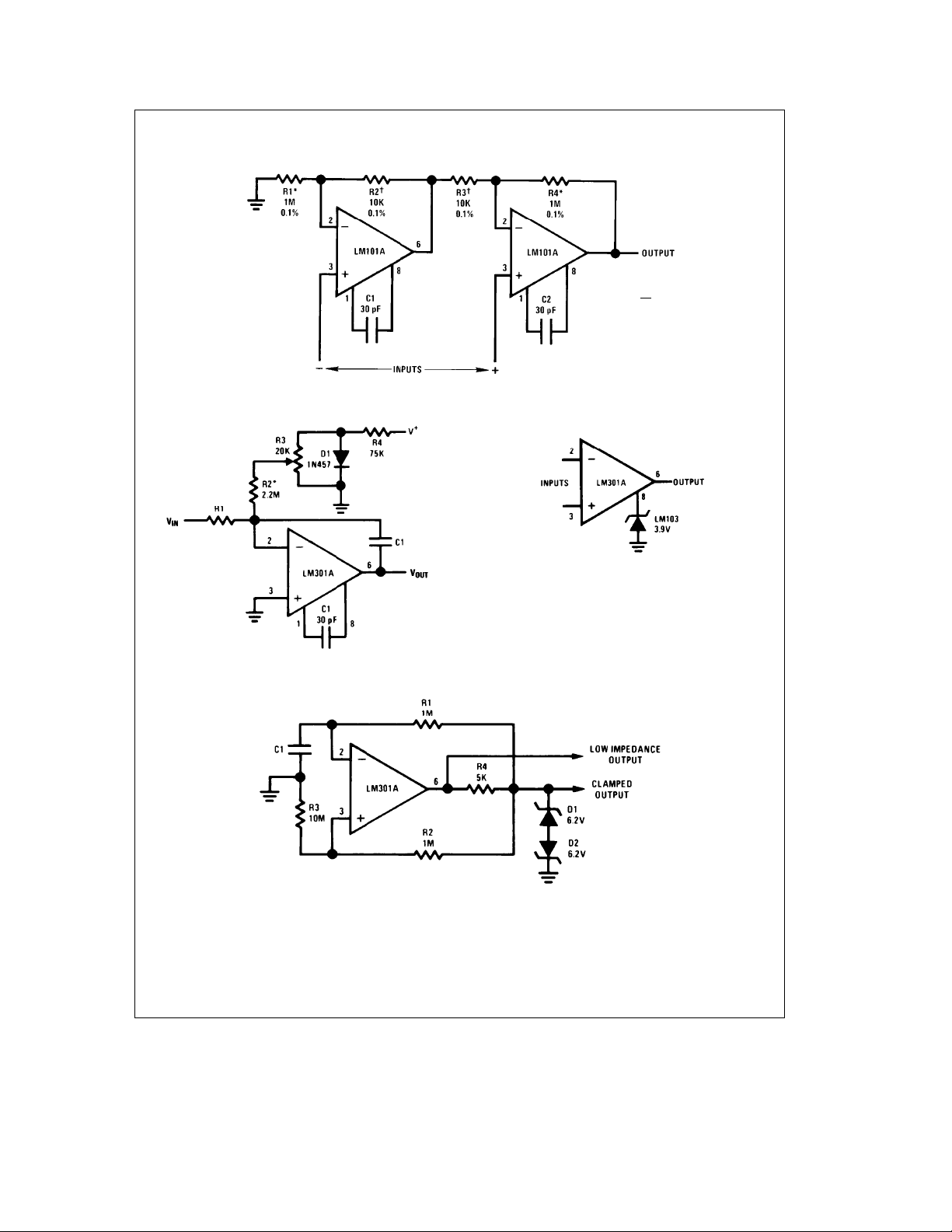
Typical Applications** (Continued)
Instrumentation Amplifier
R1eR4; R2eR3
A
²
*,
Matching determines CMRR.
e1a
V
R1
R2
TL/H/7752– 34
Integrator with Bias Current Compensation
*Adjust for zero integrator
drift. Current drift typically
0.1 nA/
temperature range.
TL/H/7752– 35
Low Frequency Square Wave Generator
C over 0§Ctoa70§C
§
Voltage Comparator for Driving RTL Logic or
High Current Driver
TL/H/7752– 37
**Pin connections shown are for 8-pin packages.
TL/H/7752– 36
9
Page 10
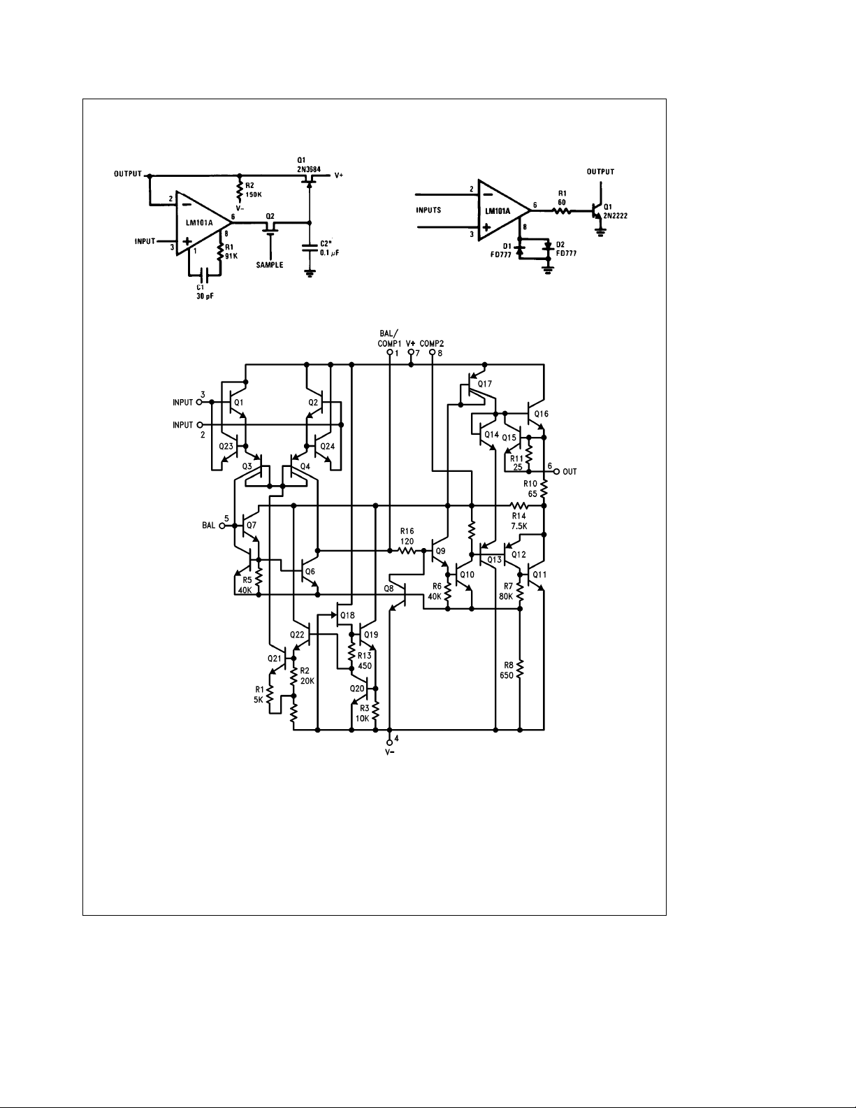
Typical Applications** (Continued)
Low Drift Sample and Hold
Voltage Comparator for Driving
DTL or TTL Integrated Circuits
Schematic**
*Polycarbonate-dielectric capacitor
TL/H/7752– 38
TL/H/7752– 39
**Pin connections shown are for 8-pin packages.
TL/H/7752– 1
10
Page 11

11
Page 12
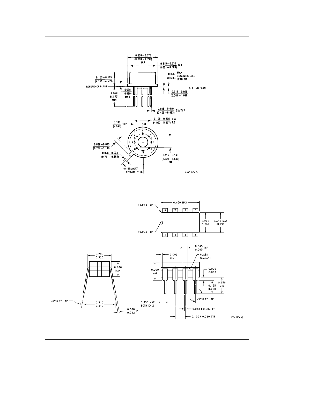
Physical Dimensions inches (millimeters)
Metal Can Package (H)
Order Number LM101AH, LM101AH/883
LM201AH or LM301AH
NS Package Number H08C
Ceramic Dual-In-Line Package (J)
Order Number LM101J/883 or LM101AJ
NS Package Number J08A
12
Page 13
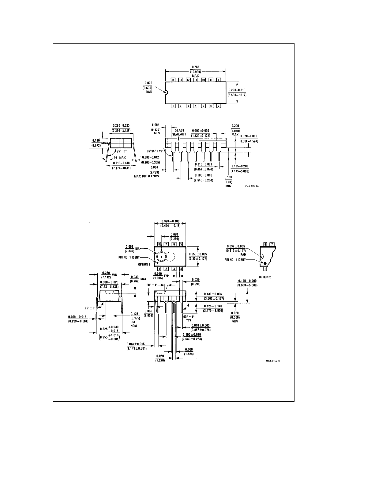
Physical Dimensions inches (millimeters) (Continued)
Ceramic Dual-In-Line Package (J)
Order Number LM101AJ-14/883
NS Package Number J14A
Molded Dual-In-Line Package (N)
Order Number LM201AN or LM301AN
NS Package Number N08E
13
Page 14
Physical Dimensions inches (millimeters) (Continued)
Ceramic Flatpack Package (W)
Order Number LM101AW/883 or LM101W/883
NS Package Number W10A
LM101A/LM201A/LM301A Operational Amplifiers
LIFE SUPPORT POLICY
NATIONAL’S PRODUCTS ARE NOT AUTHORIZED FOR USE AS CRITICAL COMPONENTS IN LIFE SUPPORT
DEVICES OR SYSTEMS WITHOUT THE EXPRESS WRITTEN APPROVAL OF THE PRESIDENT OF NATIONAL
SEMICONDUCTOR CORPORATION. As used herein:
1. Life support devices or systems are devices or 2. A critical component is any component of a life
systems which, (a) are intended for surgical implant support device or system whose failure to perform can
into the body, or (b) support or sustain life, and whose be reasonably expected to cause the failure of the life
failure to perform, when properly used in accordance support device or system, or to affect its safety or
with instructions for use provided in the labeling, can effectiveness.
be reasonably expected to result in a significant injury
to the user.
National Semiconductor National Semiconductor National Semiconductor National Semiconductor
Corporation Europe Hong Kong Ltd. Japan Ltd.
1111 West Bardin Road Fax: (
Arlington, TX 76017 Email: [email protected] Ocean Centre, 5 Canton Rd. Fax: 81-043-299-2408
Tel: 1(800) 272-9959 Deutsch Tel: (
Fax: 1(800) 737-7018 English Tel: (
National does not assume any responsibility for use of any circuitry described, no circuit patent licenses are implied and National reserves the right at any time without notice to change said circuitry and specifications.
Fran3ais Tel: (
Italiano Tel: (
a
49) 0-180-530 85 86 13th Floor, Straight Block, Tel: 81-043-299-2309
a
49) 0-180-530 85 85 Tsimshatsui, Kowloon
a
49) 0-180-532 78 32 Hong Kong
a
49) 0-180-532 93 58 Tel: (852) 2737-1600
a
49) 0-180-534 16 80 Fax: (852) 2736-9960
 Loading...