

Page 1
LM2991
Negative Low Dropout Adjustable Regulator
General Description
The LM2991 is a low dropout adjustable negative regulator
with a output voltage range between −3V to −24V. The
LM2991 providesup to 1A of load current and features a On
/Off pin for remote shutdown capability.
The LM2991 uses new circuit design techniquesto provide a
low dropout voltage, low quiescent current and low temperature coefficient precision reference. The dropout voltage at
1A load current is typically 0.6V and a guaranteed
worst-case maximum of 1V over the entire operating temperature range. The quiescent current is typically 1 mA with
a 1A load current and an input-output voltage differential
greater than 3V. A unique circuit design of the internal bias
supply limits the quiescent current to only 9 mA (typical)
when the regulator is in the dropout mode (V
OUT−VIN
≤ 3V).
The LM2991 is short-circuit proof, and thermal shutdown includes hysteresis to enhance the reliability of the device
when inadvertently overloaded for extended periods. The
LM2991 is available in 5-lead TO-220and TO-263 packages
and is rated for operation over the automotive temperature
range of −40˚C to +125˚C. Mil-Aero versions are also available.
Features
n Output voltage adjustable from −3V to −24V, typically
−2V to −25V
n Output current in excess of 1A
n Dropout voltage typically 0.6V at 1A load
n Low quiescent current
n Internal short circuit current limit
n Internal thermal shutdown with hysteresis
n TTL, CMOS compatible ON/OFF switch
n Functional complement to the LM2941 series
Applications
n Post switcher regulator
n Local, on-card, regulation
n Battery operated equipment
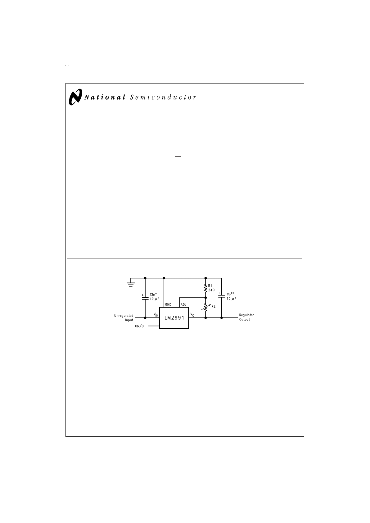
Typical Application
DS011260-1
V
OUT
=
V
REF
(1 + R2/R1)
*Required if the regulator is located further than 6 inches from the power supply filter capacitors. A 1 µF solid tantalum or a 10 µF aluminum electrolytic
capacitor is recommended.
*
*Required for stability. Must be at least a 10 µF aluminum electrolytic or a 1 µF solid tantalum to maintain stability. May be increased without bound to
maintain regulation during transients. Locate the capacitor as close as possible to the regulator. The equivalent series resistance (ESR) is critical, and
should be less than 10Ω over the same operating temperature range as the regulator.
May 1999
LM2991 Negative Low Dropout Adjustable Regulator
© 1999 National Semiconductor Corporation DS011260 www.national.com
Page 2
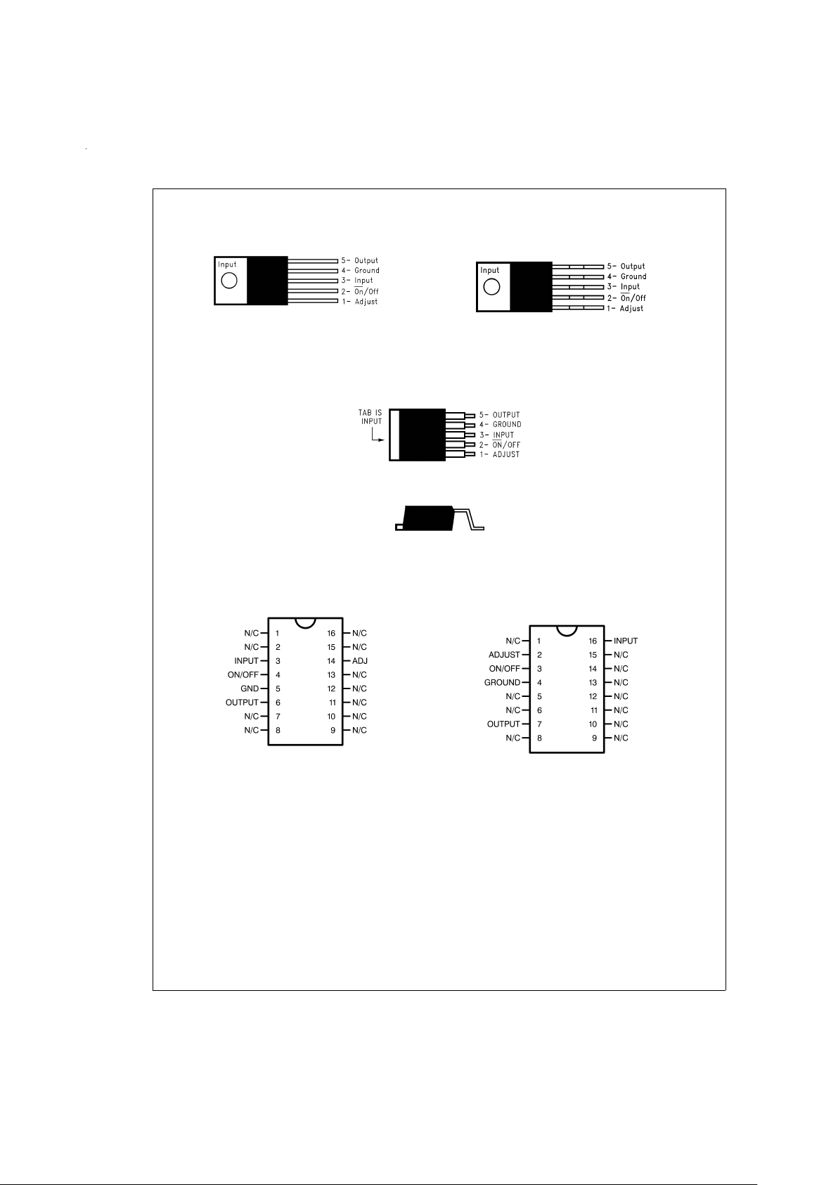
Connection Diagrams and Ordering Information
5-Lead TO-220
Straight Leads
DS011260-9
Front View
Order Number LM2991T
See NS Package Number T05A
5-Lead TO-220
Bent, Staggered Leads
DS011260-2
Front View
Order Number LM2991T Flow LB03
See NS Package Number T05D
TO263
5-Lead Surface-Mount Package
DS011260-11
Top View
DS011260-12
Side View
Order Number LM2991S
See NS Package Number TS5B
16-Lead Ceramic Dual-in-Line Package
DS011260-29
Top View
Order Number LM2991J-QMLV
5962-9650501VEA
Order Number LM2991J-QML
5962-9650501QEA
See NS Package Number J16A
16-Lead Ceramic Surface-Mount Package
DS011260-30
Top View
Order Number LM2991WG-QML
5962-9650501QXA
See NS Package Number WG16A
www.national.com 2
Page 3
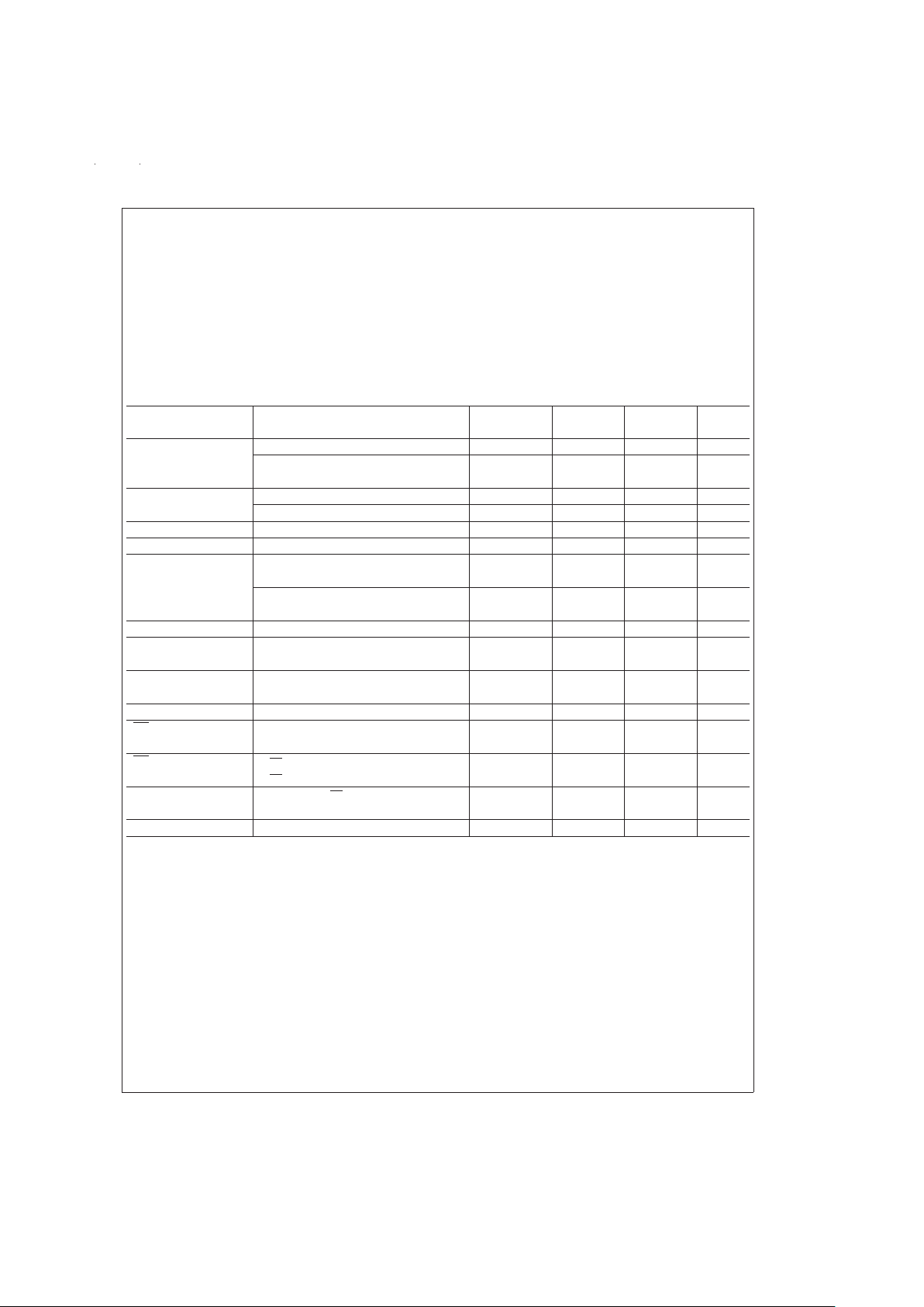
Absolute Maximum Ratings (Note 1)
If Military/Aerospace specified devices are required,
please contact the National Semiconductor Sales Office/
Distributors for availability and specifications.
Input Voltage −26V to +0.3V
ESD Susceptibility (Note 2) 2 kV
Power Dissipation (Note 3) Internally limited
Junction Temperature (T
Jmax
) 125˚C
Storage Temperature Range −65˚C to +150˚C
Lead Temperature (Soldering, 10 sec.) 230˚C
Operating Ratings (Note 1)
Junction Temperature Range (T
J
) −40˚C to +125˚C
Maximum Input Voltage (Operational) −26V
Electrical Characteristics
V
IN
=
−10V, V
O
=
−3V, I
O
=
1A, C
O
=
47 µF, R1=2.7k, T
J
=
25˚C, unless otherwise specified. Boldface limits apply over
the entire operating junction temperature range.
Parameter Conditions Typical Min Max Units
(Note 4)
Reference Voltage 5 mA ≤ I
O
≤ 1A −1.210 −1.234 −1.186 V
5mA≤I
O
≤1A, −1.27 −1.15 V
V
O
−1V≥VIN≥ −26V
Output Voltage −2 −3 V
Range V
IN
=
−26V −25 −24 V
Line Regulation I
O
=
5 mA, V
O
−1V≥VIN≥ −26V 0.004 0.04
%
/V
Load Regulation 50 mA ≤ I
O
≤ 1A 0.04 0.4
%
Dropout Voltage I
O
=
0.1A, ∆V
O
≤ 100 mV 0.1 0.2 V
0.3
I
O
=
1A, ∆V
O
≤ 100 mV 0.6 0.8 V
1
Quiescent Current I
O
≤ 1A 0.7 5 mA
Dropout Quiescent V
IN
=
V
O,IO
≤1A 16 50 mA
Current
Ripple Rejection V
ripple
=
1 Vrms,
f
ripple
=
1 kHz, 60 50 dB
I
O
=
5mA
Output Noise 10 Hz − 100 kHz, I
O
=
5 mA 200 450 µV
ON /OFF Input
(V
OUT
: ON) 1.2 0.8 V
Voltage (V
OUT
: OFF) 1.3 2.4
ON /OFF Input
V
ON/OFF
=
0.8V (V
OUT
: ON) 0.1 10 µA
Current V
ON/OFF
=
2.4V (V
OUT
: OFF) 40 100
Output Leakage V
IN
=
−26V, V
ON/OFF
=
2.4V
60 250 µA
Current V
OUT
=
0V
Current Limit V
OUT
=
0V 2 1.5 A
Note 1: Absolute Maximum Ratings indicate limits beyond which damage to the device may occur. Operating Ratings indicate conditions for which the deivce is intended to be functional, but do not guarantee specific performance limits. For guaranteed specifications and test conditions, see the Electrical Characteristics.
Note 2: Human body model, 100 pF discharged through a 1.5 kΩ resistor.
Note 3: The maximum power dissipation is a function of T
Jmax
, θJAand TA. The maximum allowable power dissipation at any ambient temperature is P
D
=
(T
Jmax
−TA)/θJA. If this dissipation is exceeded, the die temperature will rise above 125˚C and the LM2991 will go into thermal shutdown. For the LM2991, the
junction-to-ambient thermal resistance is 53˚C/W for the TO-220, 73˚C/W for the TO-263, and junction-to-case thermal resistance is 3˚C. If the TO-263 package is
used, the thermal resistance can be reduced by increasing the PC board copper area thermally connected to the package. Using 0.5 square inches of copper area,
θ
JA
is 50˚C/W; with 1 square inch of copper area, θJAis 37˚C/W; and with 1.6 or more square inches of copper area, θJAis 32˚C/W.
Note 4: Typicals are at T
J
=
25˚C and represent the most likely parametric norm.
www.national.com3
Page 4
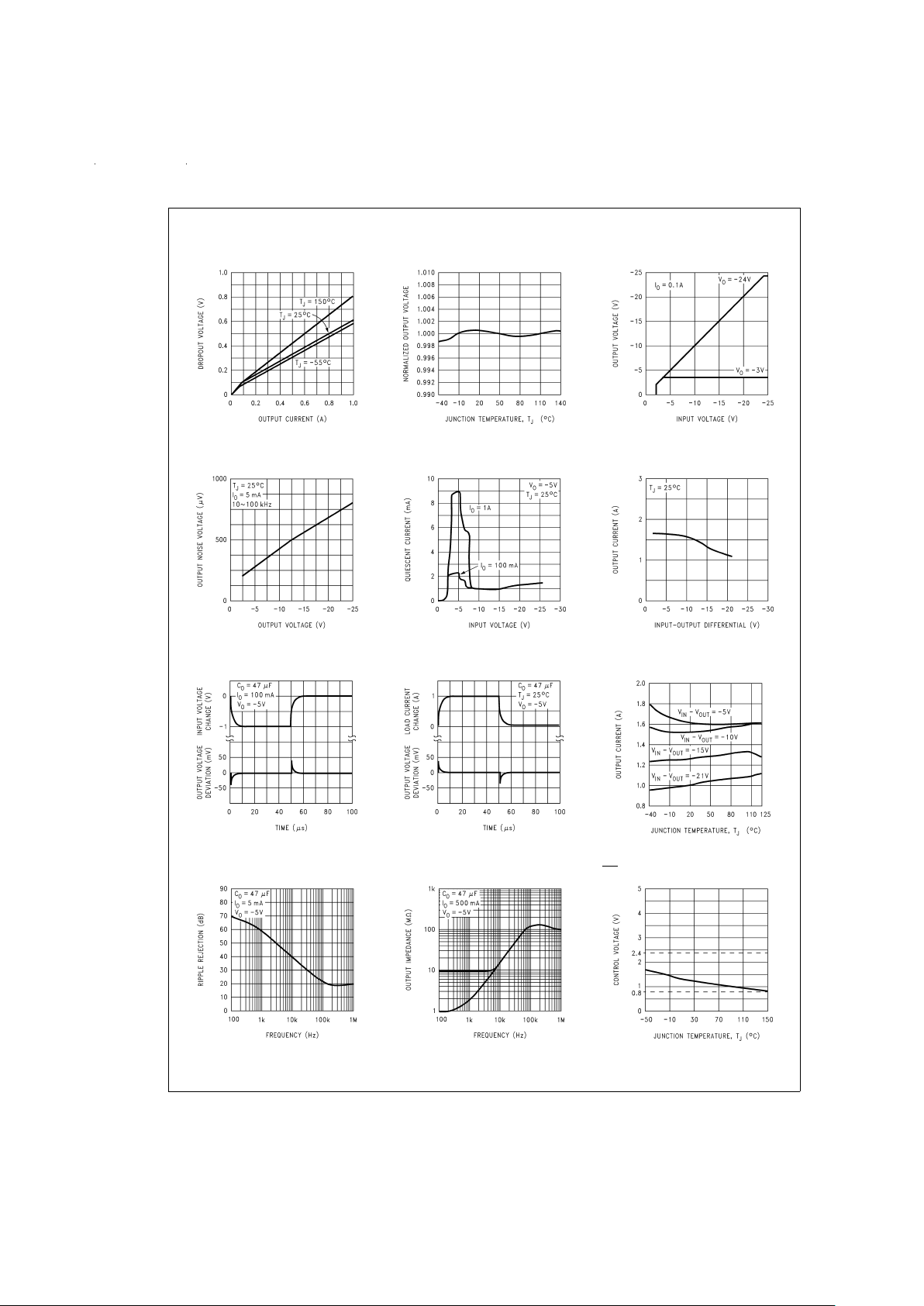
Typical Performance Characteristics
Dropout Voltage
DS011260-13
Normalized Output Voltage
DS011260-14
Output Voltage
DS011260-15
Output Noise Voltage
DS011260-16
Quiescent Current
DS011260-17
Maximum Output Current
DS011260-18
Line Transient Response
DS011260-19
Load Transient Response
DS011260-20
Maximum Output Current
DS011260-21
Ripple Rejection
DS011260-22
Output Impedance
DS011260-23
ON /OFF Control Voltage
DS011260-24
www.national.com 4
Page 5

Typical Performance Characteristics (Continued)
Application Hints
EXTERNAL CAPACITORS
The LM2991 regulator requires an output capacitor to maintain stability. The capacitor must be at least 10 µF aluminum
electrolytic or 1 µF solid tantalum. The output capacitor’s
ESR must be less than 10Ω, or the zero added to the regulator frequency response by the ESR could reduce the
phase margin, creating oscillations. The shaded area in the
Output Capacitor ESR graph indicates the recommended
ESR range. An input capacitor, of atleast 1 µF solidtantalum
or 10 µF aluminum electrolytic,is also needed if theregulator
is situated more than 6 inches from the input power supply
filter.
MINIMUM LOAD
A minimum load current of 500 µAis required for proper operation. The external resistor divider can provide the minimum load, with the resistor from the adjust pin to ground set
to 2.4 kΩ.
SETTING THE OUTPUT VOLTAGE
The output voltage of the LM2991 is set externallyby a resistor divider using the following equation:
V
OUT
=
V
REF
x(1+R2/R1)−(I
ADJxR2
)
where V
REF
=
−1.21V. The output voltage can be pro-
grammed within the range of −3V to −24V, typically an even
Adjust Pin Current
DS011260-25
Low Voltage Behavior
DS011260-26
Maximum Power
Dissipation (TO-220)
DS011260-27
Maximum Power Dissipation
(TO-263) (See Note 3)
DS011260-28
Output Capacitor ESR Range
DS011260-5
www.national.com5
Page 6

Application Hints (Continued)
greater range of −2V to −25V. The adjust pin current is about
60 nA, causing a slight error in the output voltage. However,
using resistors lower than 100 kΩ makes the adjust pin current negligible. For example, neglecting the adjust pin current, and setting R2 to 100 kΩ and V
OUT
to −5V,results in an
output voltage error of only 0.16%.
ON/OFF PIN
The LM2991 regulator can be turned off byapplying a TTL or
CMOS level high signal to the ON/OFF pin (see Adjustable
Current Sink Application).
FORCING THE OUTPUT POSITIVE
Due to an internal clamp circuit, the LM2991 can withstand
positive voltages on its output. If the voltage source pulling
the output positive is DC, the currentmust be limited to 1.5A.
A current over 1.5A fed back into the LM2991 could damage
the device. The LM2991 output can also withstand fast positive voltage transients up to 26V, without any current limiting
of the source. However, if the transients have a duration of
over 1 ms, the output should be clamped with a Schottky diode to ground.
Typical Applications
Fully Isolated Post-Switcher Regulator
DS011260-6
Adjustable Current Sink
DS011260-10
www.national.com 6
Page 7

Equivalent Schematic
DS011260-8
www.national.com7
Page 8

Physical Dimensions inches (millimeters) unless otherwise noted
5-Lead T0-220, Straight Leads (T)
Order Number LM2991T
NS Package Number T05A
5-Lead T0-220, Bent, Staggered Leads (T)
Order Number LM2991T Flow LBO3
NS Package Number T05D
www.national.com 8
Page 9

Physical Dimensions inches (millimeters) unless otherwise noted (Continued)
TO-263 5-Lead Plastic Surface Mount Package
Ordering Number LM2991S
NS Package Number TS5B
www.national.com9
Page 10

Physical Dimensions inches (millimeters) unless otherwise noted (Continued)
16-Lead Ceramic Dual-in-Line Package
Order Number LM2991J-QMLV
5962-9650501VEA
Order Number LM2991J-QML
5962-9650501QEA
NS Package Number J16A
www.national.com 10
Page 11

Physical Dimensions inches (millimeters) unless otherwise noted (Continued)
LIFE SUPPORT POLICY
NATIONAL’S PRODUCTS ARE NOT AUTHORIZED FOR USE AS CRITICAL COMPONENTS IN LIFE SUPPORT
DEVICES OR SYSTEMS WITHOUT THE EXPRESS WRITTEN APPROVAL OF THE PRESIDENT AND GENERAL
COUNSEL OF NATIONAL SEMICONDUCTOR CORPORATION. As used herein:
1. Life support devices or systems are devices or
systems which, (a) are intended for surgical implant
into the body, or (b) support or sustain life, and
whose failure to perform when properly used in
accordance with instructions for use provided in the
labeling, can be reasonably expected to result in a
significant injury to the user.
2. A critical component is any component of a life
support device or system whose failure to perform
can be reasonably expected to cause the failure of
the life support device or system, or to affect its
safety or effectiveness.
National Semiconductor
Corporation
Americas
Tel: 1-800-272-9959
Fax: 1-800-737-7018
Email: support@nsc.com
National Semiconductor
Europe
Fax: +49 (0) 1 80-530 85 86
Email: europe.support@nsc.com
Deutsch Tel: +49 (0) 1 80-530 85 85
English Tel: +49 (0) 1 80-532 78 32
Français Tel: +49 (0) 1 80-532 93 58
Italiano Tel: +49 (0) 1 80-534 16 80
National Semiconductor
Asia Pacific Customer
Response Group
Tel: 65-2544466
Fax: 65-2504466
Email: sea.support@nsc.com
National Semiconductor
Japan Ltd.
Tel: 81-3-5639-7560
Fax: 81-3-5639-7507
www.national.com
16-Lead Ceramic Surface-Mount Package
Order Number LM2991WG-QML
5962-9650501QXA
NS Package Number WG16A
LM2991 Negative Low Dropout Adjustable Regulator
National does not assume any responsibility for use of any circuitry described, no circuit patent licenses are implied and National reserves the right at any time without notice to change said circuitry and specifications.
 Loading...