

Page 1
LM2984C Microprocessor Power Supply System
General Description
The LM2984C positive voltage regulator features three independent and tracking outputs capable of delivering the
power for logic circuits, peripheral sensors and standby
memory in a typical microprocessor system. The LM2984C
includes circuitry which monitors both its own high-current
output and also an external mP. If any error conditions are
sensed in either, a reset error flag is set and maintained until
the malfunction terminates. Since these functions are included in the same package with the three regulators, a
great saving in board space can be realized in the typical
microprocessor system. The LM2984C also features very
low dropout voltages on each of its three regulator outputs
(0.6V at the rated output current). Furthermore, the quiescent current can be reduced to 1 mA in the standby mode.
Designed also for vehicular applications, the LM2984C and
all regulated circuitry are protected from reverse battery installations or 2-battery jumps. Familiar regulator features
such as short circuit and thermal overload protection are
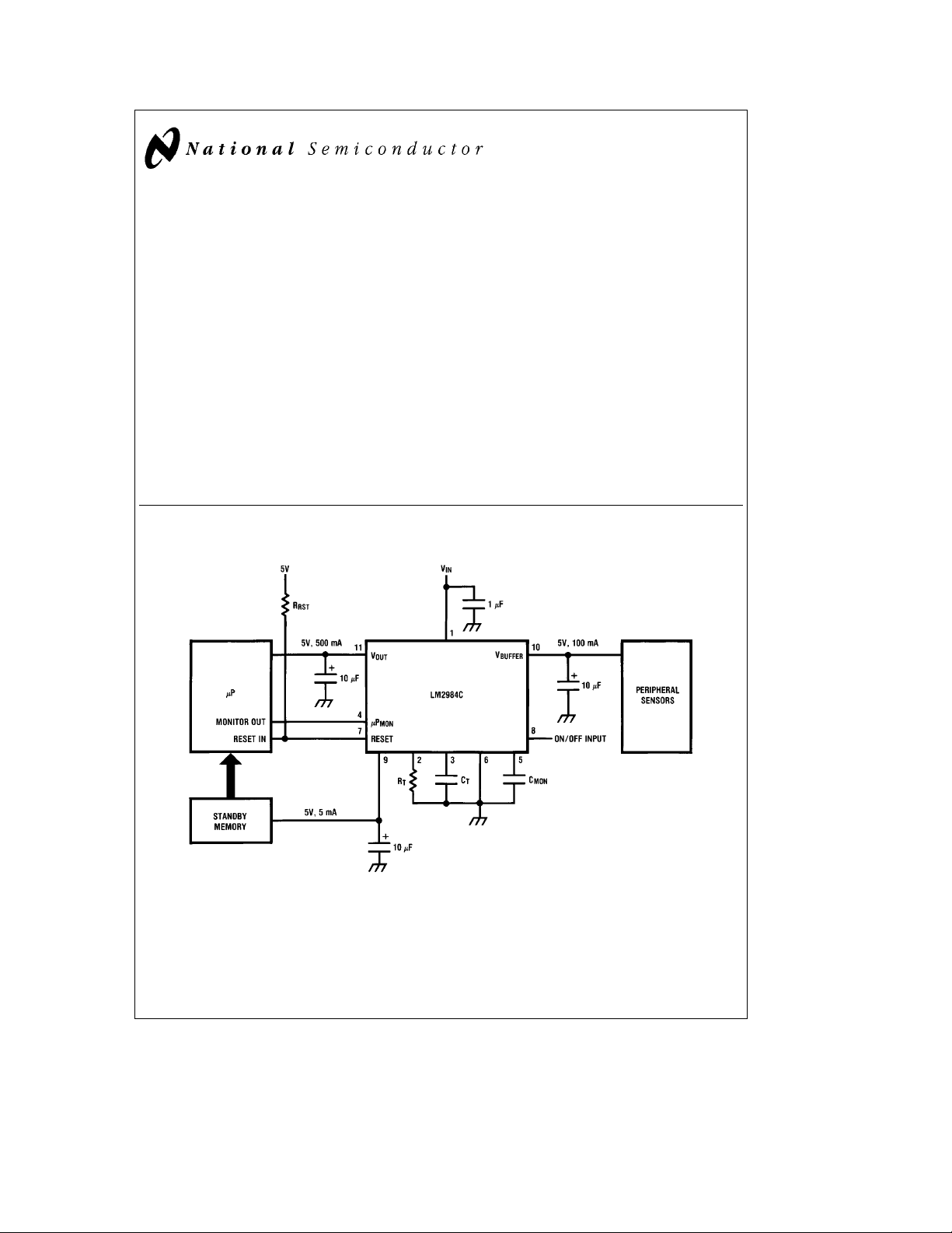
Typical Application Circuit
also provided. Fixed outputs of 5V are available in the plastic TO-220 power package.
Features
Y
Three low dropout tracking regulators
Y
Output current in excess of 500 mA
Y
Low quiescent current standby regulator
Y
Microprocessor malfunction RESET flag
Y
Delayed RESET on power-up
Y
Accurate pretrimmed 5V outputs
Y
Reverse battery protection
Y
Overvoltage protection
Y
Reverse transient protection
Y
Short circuit protection
Y
Internal thermal overload protection
Y
ON/OFF switch for high current outputs
Y
100% electrical burn-in in thermal limit
LM2984C
LM2984C Microprocessor Power Supply System
May 1989
C
must be at least 10 mFto
OUT
maintain stability. May be increased
without bound to maintain regulation
during transients. Locate as close as
possible to the regulator. This capac-
Order Number LM2984CT
See NS Package Number TA11B
C
1995 National Semiconductor Corporation RRD-B30M115/Printed in U. S. A.
TL/H/8821
itor must be rated over the same operating temperature range as the
regulator. The equivalent series resistance (ESR) of this capacitor is
critical; see curve.
TL/H/8821– 1
Page 2
Absolute Maximum Ratings
If Military/Aerospace specified devices are required,
please contact the National Semiconductor Sales
Office/Distributors for availability and specifications.
Input Voltage
Survival Voltage (
k
100 ms) 35V
Operational Voltage 26V
Internal Power Dissipation Internally Limited
Operating Temperature Range (T
)0
A
Ctoa125§C
§
Maximum Junction Temperature (Note 1) 150§C
Storage Temperature Range
b
65§Ctoa150§C
Lead Temperature (Soldering, 10 sec.) 230§C
ESD rating is to be determined.
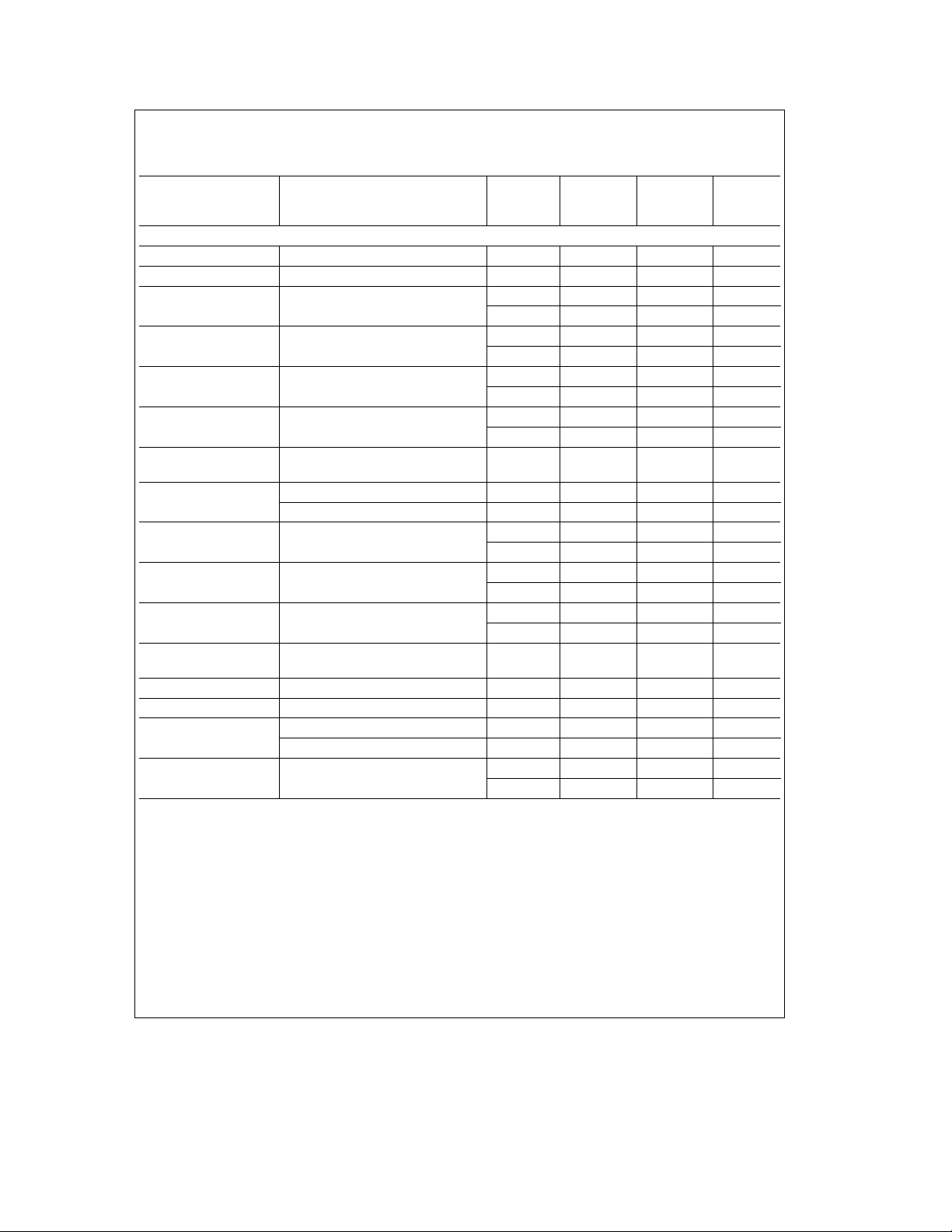
Electrical Characteristics
e
V
14V, I
IN
Parameter Conditions Typical Limit Limit Units
V
(Pin 11)
OUT
Output Voltage 5 mAsI
Line Regulation 9VsV
Load Regulation 5 mAsI
Output Impedance 250 mAdcand 10 mA
Quiescent Current I
Output Noise Voltage 10 Hz – 100 kHz, I
Long Term Stability 20 mV/1000 hr
Ripple Rejection f
Dropout Voltage I
Current Limit 0.92 0.75 A
Maximum Operational Continuous DC
Input Voltage
Maximum Line Transient V
Reverse Polarity V
Input Voltage DC
Reverse Polarity Input Ts100 ms, R
Voltage Transient
OUT
e
5 mA, C
OUT
e
10 mF, T
e
25§C (Note 6) unless otherwise indicated
j
Tested Design
(Note 2) (Note 3)
s
500 mA
o
6VsV
7VsV
f
I
I
s
26V 5.15 5.25 V
IN
s
16V 2 25 mV
IN
s
26V 5 50 mV
IN
s
500 mA 12 50 mV
OUT
,
e
120 Hz
o
e
500 mA 38 100 mA
OUT
e
250 mA 14 50 mA
OUT
e
120 Hz 70 60 dB
o
e
500 mA 0.53 0.80 1.00 V
OUT
e
250 mA 0.28 0.50 0.60 V
OUT
rms
e
100 mA 100 mV
OUT
5.00
24 mX
4.85 4.75 V
32 26 26 V
OUT
OUT
s
t
6V, R
b
OUT
0.6V, R
OUT
e
100X 45 35 35 V
e
100X
OUT
e
100X
b
30
b
55
b
15
b
35
b
15 V
b
35 V
min
max
max
max
max
max
max
min
max
max
min
min
min
min
min
2
Page 3
Electrical Characteristics (Continued)
e
V
IN
Parameter Conditions Typical Limit Limit Units
V
(Pin 10)
buffer
Output Voltage 5 mAsI
Line Regulation 9VsV
Load Regulation 5 mAsI
Output Impedance 50 mAdcand 10 mA
Quiescent Current I
Output Noise Voltage 10 Hz–100 kHz, I
Long Term Stability 20 mV/1000 hr
Ripple Rejection f
Dropout Voltage I
Current Limit 0.23 0.15 A
Maximum Operational Continuous DC
Input Voltage
Maximum Line V
Transient
Reverse Polarity V
Input Voltage DC
Reverse Polarity Input Ts100 ms, R
Voltage Transient
14V, I
buf
e
5 mA, C
buf
e
10 mF, T
e
25§C (Note 6) unless otherwise indicated
j
Tested Design
(Note 2) (Note 3)
s
100 mA
o
6VsV
7VsV
s
26V 5.15 5.25 V
IN
s
16V 2 25 mV
IN
s
26V 5 50 mV
IN
s
100 mA 15 50 mV
buf
, 200 mX
rms
e
100 mA 8.0 15.0 mA
buf
e
100 mA 100 mV
OUT
e
120 Hz 70 60 dB
o
e
100 mA 0.35 0.50 0.60 V
buf
5.00
4.85 4.75 V
32 26 26 V
buf
buf
s
t
6V, R
b
0.6V, R
buf
buf
e
buf
100X
e
e
100X
100X
45 35 35 V
b
30
b
55
b
15
b
35
b
b
15 V
35 V
min
max
max
max
max
max
min
max
min
min
min
min
min
Electrical Characteristics
e
V
14V, I
IN
Parameter Conditions Typical Limit Limit Units
V
(Pin 9)
standby
Output Voltage 1 mAsI
Line Regulation 9VsV
Load Regulation 0.5 mAsI
Output Impedance 5 mAdcand1mA
Quiescent Current I
stby
e
1 mA, C
stby
e
10 mF, T
e
25§C (Note 6) unless otherwise indicated
j
Tested Design
(Note 2) (Note 3)
s
7.5 mA
o
6VsV
7VsV
I
s
26V 5.15 5.25 V
IN
s
16V 2 25 mV
IN
s
26V 5 50 mV
IN
s
7.5 mA 6 50 mV
stby
e
120 Hz 0.9 X
rms,fo
e
7.5 mA 1.2 2.0 mA
stby
e
2 mA 0.9 1.5 mA
stby
5.00
4.85 4.75 V
3
min
max
max
max
max
max
max
Page 4
Electrical Characteristics (Continued)
e
14V, I
V
IN
Parameter Conditions Typical Limit Limit Units
V
(Continued)
standby
Output Noise Voltage 10 Hz –100 kHz, I
Long Term Stability 20 mV/1000 hr
Ripple Rejection f
Dropout Voltage I
Dropout Voltage I
Current Limit 15 12 mA
Maximum Operational 4.5VsV
Input Voltage R
Maximum Line V
Transient R
Reverse Polarity V
Input Voltage DC R
Reverse Polarity Input Ts100 ms, R
Voltage Transient
stby
e
1 mA, C
stby
e
10 mF, T
e
25§C (Note 6) unless otherwise indicated
j
Tested Design
(Note 2) (Note 3)
e
1 mA 100 mV
stby
e
120 Hz 70 60 dB
o
e
1 mA 0.26 0.50 0.50 V
stby
e
7.5 mA 0.38 0.60 0.70 V
stby
s
6V
stby
stby
stby
stby
stby
e
s
e
t
e
stby
1000X
6V,
1000X
b
0.6V,
1000X
stby
e
1000X
45 35 35 V
45 35 35 V
b
30
b
55
b
15
b
35
b
b
15 V
35 V
Electrical Characteristics
e
V
IN
Parameter Conditions Typical Limit Limit Units
Tracking and Isolation
Tracking I
V
OUT–Vstby
Tracking I
V
buf–Vstby
Tracking I
V
OUT–Vbuf
Isolation* R
V
buf
Isolation* R
V
stby
Isolation* R
V
OUT
Isolation* R
V
stby
*Isolation refers to the ability of the specified output to remain within the tested limits when the other output is shorted to ground.
14V, T
from V
from V
from V
from V
e
25§C (Note 6) C
j
OUT
OUT
buf
buf
OUT
I
stby
OUT
I
stby
OUT
I
stby
OUT
OUT
buf
buf
OUT
s
500 mA, I
s
7.5 mA
e
5 mA, I
s
7.5 mA
s
500 mA, I
e
1mA
e
e
e
1X,I
e
1X,I
e
1X,I
1X,I
10 mF, C
buf
buf
buf
s
buf
stby
s
OUT
s
stby
e
s
100 mA,
s
100 mA
s
7.5 mA
500 mA
7.5 mA
e
buf
5 mA,
100 mA,
10 mF, C
e
10 mF unless otherwise specified
stby
Tested Design
(Note 2) (Note 3)
g
g
g
5.00
5.00
5.00
5.00
30
30
30
g
g
g
4.50 V
5.50 V
4.50 V
5.50 V
4.50 V
5.50 V
4.50 V
5.50 V
100 mV
100 mV
100 mV
min
max
max
min
min
min
min
min
max
max
max
min
max
min
max
min
max
min
max
4
Page 5
Electrical Characteristics (Continued)
e
14V, I
V
IN
otherwise specified
Parameter Conditions Typical Limit Limit Units
Computer Monitor/Reset Functions
I
Low V
reset
V
Low V
reset
R
t voltage
Power On Reset VmP
Delay (T
V
Low (Note 4) 4.00 3.60 V
OUT
Reset Threshold
V
High (Note 4) 5.50 5.25 V
OUT
Reset Threshold
Reset Output VmP
Leakage
mP
Input VmP
mon
Current (Pin 4)
mP
Input 1.22 0.80 0.80 V
mon
Threshold Voltage
mP Monitor Reset VmP
Oscillator Period (T
mP Monitor Reset VmP
Oscillator Pulse Width (RESET
Minimum mP Monitor (Note 5)
Input Pulse Width
Reset Fall Time R
Reset Rise Time R
On/Off Switch Input V
Current (Pin 8)
On/Off Switch Input 1.22 0.80 0.80 V
Threshold Voltage
Note 1: Thermal resistance without a heatsink for junction-to-case temperature is 3§C/W. Thermal resistance case-to-ambient is 40§C/W.
Note 2: Tested Limits are guaranteed and 100% production tested.
Note 3: Design Limits are guaranteed (but not 100% production tested) over the indicated temperature and supply voltage range. These limits are not used to
calculate outgoing quality levels.
Note 4: An internal comparator detects when the main regulator output (V
Reset Error Flag is held low until the error condition has terminated. The Reset Error Flag is then allowed to go high again after a delay set by R
Applications Section.)
Note 5: This parameter is a measure of how short a pulse can be detected at the mP Monitor Input. This parameter is primarily influenced by the value of C
(See Typical Performance Characteristics and Applications Section.)
Note 6: To ensure constant junction temperature, low duty cycle pulse testing is used.
OUT
e
5 mA, I
buf
e
5 mA, I
stby
e
5 mA, R
t
e
130k, C
e
t
0.33 mF, C
mon
e
0.47 mF, T
Tested Design
(Note 2) (Note 3)
e
IN
e
IN
4V, V
4V, I
e
0.4V 5 2 1 mA
rst
e
1 mA 0.10 0.40 V
rst
(Pin 2) 1.22 1.15 V
1.22 1.30 V
e
5V 50 45 ms
mon
e
1.2 RtCt)
dly
50 55 ms
4.00 4.40 V
5.50 6.00 V
VmP
mon
mon
mon
e
e
e
e
5V, V
12V
rst
0.01 1 mA
2.4V 7.5 25 mA
0.4V 0.01 10 mA
1.22 2.00 2.00 V
e
0V 50 45 ms
mon
e
window
0.82 RtC
e
0V 1.0 0.7 0.5 ms
mon
e
2000 C
pw
mon
mon
)
)
50 55 ms
1.0 1.3 2.0 ms
2 ms
e
rst
e
rst
e
ON
e
V
ON
e
10k, V
rst
e
10k, V
rst
2.4V 7.5 25 mA
0.4V 0.01 10 mA
5V, C
5V, C
s
10 pF 0.20 1.00 ms
rst
s
10 pF 0.60 1.00 ms
rst
1.22 2.00 2.00 V
) drops below 4.0V or rises above 5.5V. If either condition exists at the output, the
OUT
e
25§C (Note 6) unless
j
t
and Ct. (See
max
min
max
max
min
max
min
max
max
max
max
min
max
max
max
max
max
max
max
max
min
max
min
min
min
min
mon
.
5
Page 6

Block Diagram
Pin Description
Pin No. Pin Name Comments
1VINPositive supply input voltage
2R
3C
4 mP
5C
6 Ground Regulator ground
t
t
mon
mon
Sets internal timing currents
Sets power-up reset delay timing
Microcomputer monitor input
Sets mC monitor timing
7 Reset Reset error flag output
8 ON/OFF Enables/disables high current regulators
9V
10 V
11 V
standby
buffer
OUT
Standby regulator output (7.5 mA)
Buffer regulator output (100 mA)
Main regulator output (500 mA)
TL/H/8821– 2
External Components
Component Typical Value Component Range Comments
C
IN
R
t
C
t
C
tc
R
tc
C
mon
R
rst
C
stby
C
buf
C
OUT
1 mF 0.47 mF–10 mF Required if device is located far from power supply filter.
130k 24k –1.2M Sets internal timing currents.
0.33 mF 0.033 mF– 3.3 mF Sets power-up reset delay.
0.01 mF 0.001 mF– 0.1 mF Establishes time constant of AC coupled computer monitor.
10k 1k–100k Establishes time constant of AC coupled computer monitor. (See
applications section.)
0.47 mF 0.047 mF– 4.7 mF Sets time window for computer monitor. Also determines period and pulse
width of computer malfunction reset. (See applications section.)
10k 5k–100k Load for open collector reset output. Determined by computer reset input
requirements.
10 mF10mF– no bound A 10 mF is required for stability but larger values can be used to maintain
regulation during transient conditions.
10 mF10mF– no bound A 10 mF is required for stability but larger values can be used to maintain
regulation during transient conditions.
10 mF10mF– no bound A 10 mF is required for stability but larger values can be used to maintain
regulation during transient conditions.
6
Page 7

Typical Circuit Waveforms
Connection Diagram
TL/H/8821– 3
TL/H/8821– 4
Order Number LM2984CT
See NS Package Number TA11B
7
Page 8

Typical Performance Characteristics
Dropout Voltage (V
Dropout Voltage (V
OUT
OUT
Peak Output Current (V
) Dropout Voltage (V
) Dropout Voltage (V
) Peak Output Current (V
OUT
) Dropout Voltage (V
buf
) Dropout Voltage (V
buf
) Peak Output Current (V
buf
stby
stby
)
)
stby
)
Quiescent Current (V
) Quiescent Current (V
OUT
8
) Quiescent Current (V
buf
)
stby
TL/H/8821– 5
Page 9

Typical Performance Characteristics (Continued)
Quiescent Current (V
Quiescent Current (V
Output Voltage (V
OUT
) Quiescent Current (V
OUT
) Quiescent Current (V
OUT
) Output Voltage (V
) Quiescent Current (V
buf
) Quiescent Current (V
buf
) Output Voltage (V
buf
stby
stby
stby
)
)
)
Low Voltage Behavior (V
) Low Voltage Behavior (V
OUT
9
) Low Voltage Behavior (V
buf
stby
TL/H/8821– 6
)
Page 10

Typical Performance Characteristics (Continued)
Line Transient
Response (V
OUT
)
Load Transient
Response (V
OUT
)
Output Impedance (V
Line Transient
Response (V
Load Transient
Response (V
) Output Impedance (V
OUT
buf
buf
)
Response (V
Load Transient
Line Transient
)
) Output Impedance (V
buf
Response (V
stby
stby
)
)
)
stby
Ripple Rejection (V
) Ripple Rejection (V
OUT
10
) Ripple Rejection (V
buf
)
stby
TL/H/8821– 7
Page 11

Typical Performance Characteristics (Continued)
Output Voltage
Device Dissipation vs
Ambient Temperature
TL/H/8821– 8
Output Capacitor ESR
(Standby Output, Pin 9)
TL/H/8821– 13
Output Capacitor ESR
(Buffer Output, Pin 10)
Application Hints
OUTPUT CAPACITORS
The LM2984C output capacitors are required for stability.
Without them, the regulator outputs will oscillate, sometimes
by many volts. Though the 10 mF shown are the minimum
recommended values, actual size and type may vary depending upon the application load and temperature range.
Capacitor effective series resistance (ESR) also affects the
IC stability. Since ESR varies from one brand to the next,
some bench work may be required to determine the minimum capacitor value to use in production. Worst case is
usually determined at the minimum ambient temperature
and the maximum load expected.
Output capacitors can be increased in size to any desired
value above the minimum. One possible purpose of this
would be to maintain the output voltages during brief conditions of negative input transients that might be characteristic of a particular system.
Capacitors must also be rated at all ambient temperatures
expected in the system. Many aluminum type electrolytics
will freeze at temperatures less than
effective capacitance to zero. To maintain regulator stability
b
down to
40§C, capacitors rated at that temperature (such
as tantalums) must be used.
Each output must be terminated by a capacitor, even if it is
not used.
STANDBY OUTPUT
The standby output is intended for use in systems requiring
standby memory circuits. While the high current regulator
b
30§C, reducing their
TL/H/8821– 9
Output Capacitor ESR
(Main Output, Pin 11)
TL/H/8821– 14
TL/H/8821– 15
outputs are controlled with the ON/OFF pin described later,
the standby output remains on under all conditions as long
as sufficient input voltage is supplied to the IC. Thus, memory and other circuits powered by this output remain unaffected by positive line transients, thermal shutdown, etc.
The standby regulator circuit is designed so that the quiescent current to the IC is very low (
k
1.5 mA) when the other
regulator outputs are off.
The capacitor on the output of this regulator can be increased without bound. This will help maintain the output
voltage during negative input transients and will also help to
reduce the noise on all three outputs. Because the other
two track the standby output: therefore any noise reduction
here will also reduce the other two noise voltages.
BUFFER OUTPUT
The buffer output is designed to drive peripheral sensor circuitry in a mP system. It will track the standby and main
regulator within a few millivolts in normal operation. Therefore, a peripheral sensor can be powered off this supply and
have the same operating voltage as the mP system. This is
important if a ratiometric sensor system is being used.
The buffer output can be short circuited while the other two
outputs are in normal operation. This protects the mP system from disruption of power when a sensor wire, etc. is
temporarily shorted to ground, i.e. only the sensor signal
would be interrupted, while the mP and memory circuits
would remain operational.
The buffer output is similar to the main output in that it is
controlled by the ON/OFF switch in order to save power in
11
Page 12

Application Hints (Continued)
the standby mode. It is also fault protected against overvoltage and thermal overload. If the input voltage rises above
approximately 30V (e.g. load dump), this output will automatically shut down. This protects the internal circuitry and
enables the IC to survive higher voltage transients than
would otherwise be expected. Thermal shutdown is necessary since this output is one of the dominant sources of
power dissipation in the IC.
MAIN OUTPUT
The main output is designed to power relatively large loads,
i.e. approximately 500 mA. It is therefore also protected
against overvoltage and thermal overload.
This output will track the other two within a few millivolts in
normal operation. It can therefore be used as a reference
voltage for any signal derived from circuitry powered off the
standby or buffer outputs. This is important in a ratiometric
sensor system or any system requiring accurate matching of
power supply voltages.
ON/OFF SWITCH
The ON/OFF switch controls the main output and the buffer
output. The threshold voltage is compatible with most logic
families and has about 20 mV of hysteresis to insure ‘clean’
switching from the standby mode to the active mode and
vice versa. This pin can be tied to the input voltage through
a10kXresistor if the regulator is to be powered continu-
ously.
POWER DOWN OVERRIDE
Another possible approach is to use a diode in series with
the ON/OFF signal and another in series with the main output in order to maintain power for some period of time after
the ON/OFF signal has been removed (see
the ON/OFF switch is initially pulled high through diode D1,
the main output will turn on and supply power through diode
D2 to the ON/OFF switch effectively latching the main output. An open collector transistor Q1 is connected to the
ON/OFF pin along with the two diodes and forces the regulators off after a period of time determined by the mP. In this
way, the mP can override a power down command and store
data, do housekeeping, etc. before reverting back to the
standby mode.
Figure 1
). When
DELAYED RESET
Resistor R
RESET output is held low after a main output error condition
and capacitor Ctset the period of time that the
t
has been sensed. The delay is given by the formula:
e
T
1.2 RtCt(seconds)
dly
The delayed RESET will be initiated any time the main output is outside the 4V to 5.5V window, i.e. during power-up,
short circuit, overvoltage, low line, thermal shutdown or
power-down. The mP is therefore RESET whenever the output voltage is out of regulation. (It is important to note that a
RESET is only initiated when the main output is in error. The
buffer and standby outputs are not directly monitored for
error conditions.)
mP MONITOR RESET
There are two distinct and independent error monitoring
systems in the LM2984C. The one described above monitors the main regulator output and initiates a delayed RESET whenever this output is in error. The other error monitoring system is the mP watchdog. These two systems are
OR’d together internally and both force the RESET output
low when either type of error occurs.
This watchdog circuitry continuously monitors a pin on the
mP that generates a positive going pulse during normal operation. The period of this pulse is typically on the order of
milliseconds and the pulse width is typically on the order of
10’s of microseconds. If this pulse ever disappears, the
watchdog circuitry will time out and a RESET low will be
sent to the mP. The time out period is determined by two
external components, R
la:
T
window
The width of the RESET pulse is set by C
nal resistor according to the following:
RESET
e
pw
and C
t
0.82 RtC
e
2000 C
, according to the formu-
mon
(seconds)
mon
mon
mon
(seconds)
and an inter-
A square wave signal can also be monitored for errors by
filtering the C
the signal are detected.
input such that only the positive edges of
mon
Figure 2
is a schematic diagram of a
typical circuit used to differentiate the input signal. Resistor
R
and capacitor Ctcpass only the rising edge of the
tc
square wave and create a short positive pulse suitable for
the mP monitor input. If the incoming signal continues in a
high state or in a low state for too long a period of time, a
RESET low will be generated.
FIGURE 1. Power Down Override
TL/H/8821– 10
RESET OUTPUT
This output is an open collector NPN transistor which is
forced low whenever an error condition is present at the
main output or when a mP error is sensed (see mP Monitor
section). If the main output voltage drops below 4V or rises
above 5.5V, the RESET output is forced low and held low
for a period of time set by two external components, R
C
. There is a slight amount of hysteresis in these two
t
threshold voltages so that the RESET output has a fast rise
and
t
and fall time compatible with the requirements of most mP
RESET inputs.
FIGURE 2. Monitoring Square Wave mP Signals
TL/H/8821– 11
The threshold voltage and input characteristics of this pin
are compatible with nearly all logic families.
There is a limit on the width of a pulse that can be reliably
detected by the watchdog circuit. This is due to the output
resistance of the transistor which discharges C
high state is detected at the input. The minimum detectable
mon
pulse width can be determined by the following formula:
e
PW
min
20 C
mon
(seconds)
12
when a
Page 13

Equivalent Schematic Diagram
TL/H/8821– 12
13
Page 14

Physical Dimensions inches (millimeters) Lit.
LM2984C Microprocessor Power Supply System
Molded TO-220 Package (TA)
Order Number LM2984CT
NS Package Number TA11A
Ý
108032-1
LIFE SUPPORT POLICY
NATIONAL’S PRODUCTS ARE NOT AUTHORIZED FOR USE AS CRITICAL COMPONENTS IN LIFE SUPPORT
DEVICES OR SYSTEMS WITHOUT THE EXPRESS WRITTEN APPROVAL OF THE PRESIDENT OF NATIONAL
SEMICONDUCTOR CORPORATION. As used herein:
1. Life support devices or systems are devices or 2. A critical component is any component of a life
systems which, (a) are intended for surgical implant support device or system whose failure to perform can
into the body, or (b) support or sustain life, and whose be reasonably expected to cause the failure of the life
failure to perform, when properly used in accordance support device or system, or to affect its safety or
with instructions for use provided in the labeling, can effectiveness.
be reasonably expected to result in a significant injury
to the user.
National Semiconductor National Semiconductor National Semiconductor National Semiconductor
Corporation Europe Hong Kong Ltd. Japan Ltd.
1111 West Bardin Road Fax: (
Arlington, TX 76017 Email: cnjwge@tevm2.nsc.com Ocean Centre, 5 Canton Rd. Fax: 81-043-299-2408
Tel: 1(800) 272-9959 Deutsch Tel: (
Fax: 1(800) 737-7018 English Tel: (
National does not assume any responsibility for use of any circuitry described, no circuit patent licenses are implied and National reserves the right at any time without notice to change said circuitry and specifications.
Fran3ais Tel: (
Italiano Tel: (
a
49) 0-180-530 85 86 13th Floor, Straight Block, Tel: 81-043-299-2309
a
49) 0-180-530 85 85 Tsimshatsui, Kowloon
a
49) 0-180-532 78 32 Hong Kong
a
49) 0-180-532 93 58 Tel: (852) 2737-1600
a
49) 0-180-534 16 80 Fax: (852) 2736-9960
 Loading...