

Page 1
LM2941/LM2941C
1A Low Dropout Adjustable Regulator
General Description
The LM2941 positive voltage regulator features the ability to
source 1A of output current with a typical dropout voltage of
0.5V and a maximum of 1V over the entire temperature
range. Furthermore,aquiescent current reduction circuit has
been included which reduces the ground pin current when
the differentialbetween the input voltage and the output voltage exceeds approximately 3V. The quiescent current with
1A of output current and an input-output differential of 5V is
therefore only 30 mA. Higher quiescent currents only exist
when the regulator is inthe dropout mode (V
IN−VOUT
≤ 3V).
Designed also for vehicular applications, the LM2941 and all
regulated circuitry are protected from reverse battery installations or two-battery jumps. During line transients, such as
load dump when the input voltage can momentarily exceed
the specified maximum operating voltage, the regulator will
automatically shut down to protect both the internal circuits
and theload. Familiar regulator features such as short circuit
and thermal overload protection are also provided.
Features
n Output voltage adjustable from 5V to 20V
n Dropout voltage typically 0.5V
@
I
O
=
1A
n Output current in excess of 1A
n Trimmed reference voltage
n Reverse battery protection
n Internal short circuit current limit
n Mirror image insertion protection
n P
+
Product Enhancement tested
n TTL, CMOS compatible ON/OFF switch
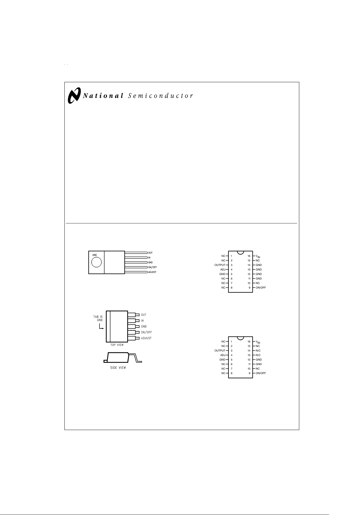
Connection Diagram and Ordering Information
TO-220 Plastic Package
DS008823-2
Front View
Order Number LM2941T or LM2941CT
See NS Package Number TO5A
TO-263 Surface-Mount Package
DS008823-8
DS008823-9
Order Number LM2941S or LM2941CS
See NS Package Number TS5B
16-Lead Ceramic Dual-in-Line Package
DS008823-31
Top View
Order Number LM2941J/883
5962-9166701QEA
See NS Package Number J16A
16-Lead Ceramic Surface Mount Package
DS008823-32
Front View
Order Number LM2941WG/883
5962-9166701QYA
See NS Package Number WG16A
June 1999
LM2941/LM2941C 1A Low Dropout Adjustable Regulator
© 1999 National Semiconductor Corporation DS008823 www.national.com
Page 2
Absolute Maximum Ratings (Note 1)
If Military/Aerospace specified devices are required,
please contact the National Semiconductor Sales Office/
Distributors for availability and specifications.
Input Voltage (Survival Voltage, ≤ 100 ms)
LM2941T, LM2941S 60V
LM2941CT, LM2941CS 45V
Internal Power Dissipation (Note 3) Internally Limited
Maximum Junction Temperature 150˚C
Storage Temperature Range −65˚C ≤ T
J
≤ +150˚C
Lead Temperature
(Soldering, 10 seconds)
TO-220 (T) Package 260˚C
TO-263 (S) Package 260˚C
ESD susceptibility to be determined.
Operating Ratings
Maximum Input Voltage 26V
Temperature Range
LM2941T −40˚C ≤ T
J
≤ 125˚C
LM2941CT 0˚C ≤ T
J
≤ 125˚C
LM2941S −40˚C ≤ T
J
≤ 125˚C
LM2941CS 0˚C ≤ T
J
≤ 125˚C
LM2941J −55˚C ≤ T
J
≤ 125˚C
LM2941WG −55˚C ≤ T
J
≤ 125˚C
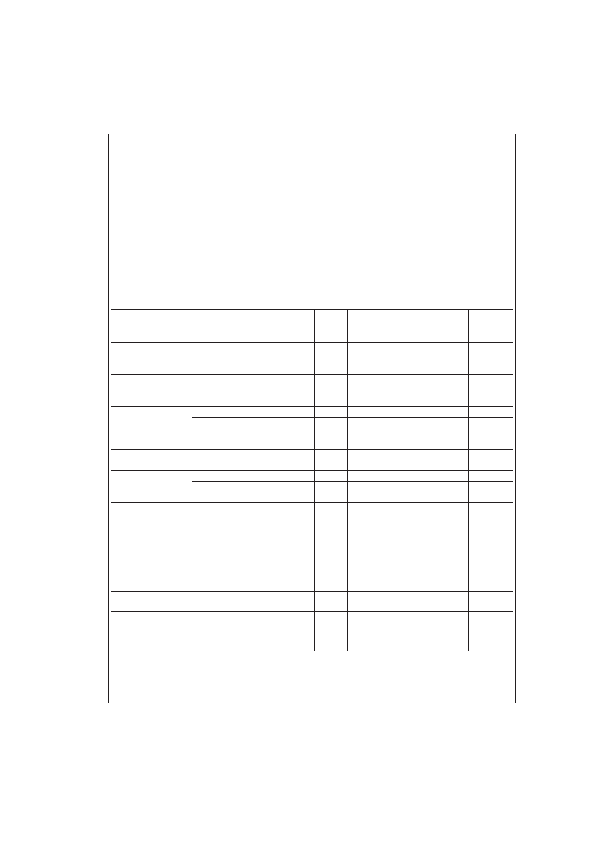
Electrical Characteristics—LM2941T, LM2941S, LM2941J, LM2941WG
5V ≤ VO≤ 20V, V
IN
=
V
O
+ 5V, C
O
=
22 µF, unless otherwise specified. Specifications in standard typeface apply for T
J
=
25˚C, while those in boldface type apply over the full Operating Temperature Range.
Parameter Conditions Typ
LM2941J
LM2941WG
Limit
(Note 2) (Note 4)
LM2941T
LM2941S
Limit
(Note 5)
Units
(Limits)
Reference Voltage 5 mA ≤ I
O
≤ 1A (Note 6) 1.275 1.237/1.211 1.237/1.211 V(min)
1.313/1.339 1.313/1.339 V(max)
Line Regulation V
O
+2V≤VIN≤ 26V, I
O
=
5 mA 4 10/10 10/10 mV/V(max)
Load Regulation 50 mA ≤ I
O
≤ 1A 7 10/10 10/10 mV/V(max)
Output Impedance 100 mADC and 20 mArms 7 mΩ/V
f
O
=
120 Hz
Quiescent Current V
O
+2V≤V
IN
<
26V, I
O
=
5 mA 10 15/20 15/20 mA(max)
V
IN
=
V
O
+ 5V, I
O
=
1A 30 45/60 45/60 mA(max)
RMS Output Noise, 10 Hz–100 kHz 0.003
%
%
of V
OUT
I
O
=
5mA
Ripple Rejection f
O
=
120 Hz, 1 Vrms, I
L
=
100 mA 0.005 0.02/0.04 0.02/0.04
%
/V(max)
Long Term Stability 0.4
%
/1000 Hr
Dropout Voltage I
O
=
1A 0.5 0.8/1.0 0.8/1.0 V(max)
I
O
=
100 mA 110 200/200 200/200 mV(max)
Short Circuit Current V
IN
max=26V (Note 7) 1.9 1.6/1.3 1.6 A(min)
Maximum Line V
O
max 1V above nominal V
O
75 60/60 60/60 V(min)
Transient R
O
=
100Ω,T≤100 ms
Maximum Operational
Input Voltage
31 26/26 26/26 V
DC
Reverse Polarity DC
Input Voltage
R
O
=
100Ω,V
O
≥−0.6V
−30 −15/−15 −15/−15 V(min)
Reverse Polarity
Transient Input
Voltage
T ≤ 100 ms, R
O
=
100Ω
−75 −50/−50 −50/−50 V(min)
ON/OFF Threshold
Voltage ON
I
O
≤ 1A 1.30 0.80/0.80 0.80/0.80 V(max)
ON/OFF Threshold
Voltage OFF
I
O
≤ 1A 1.30 2.00/2.00 2.00/2.00 V(min)
ON/OFF Threshold
Current
V
ON/OFF
=
2.0V, I
O
≤ 1A
50 100/300 100/300 µA(max)
www.national.com 2
Page 3
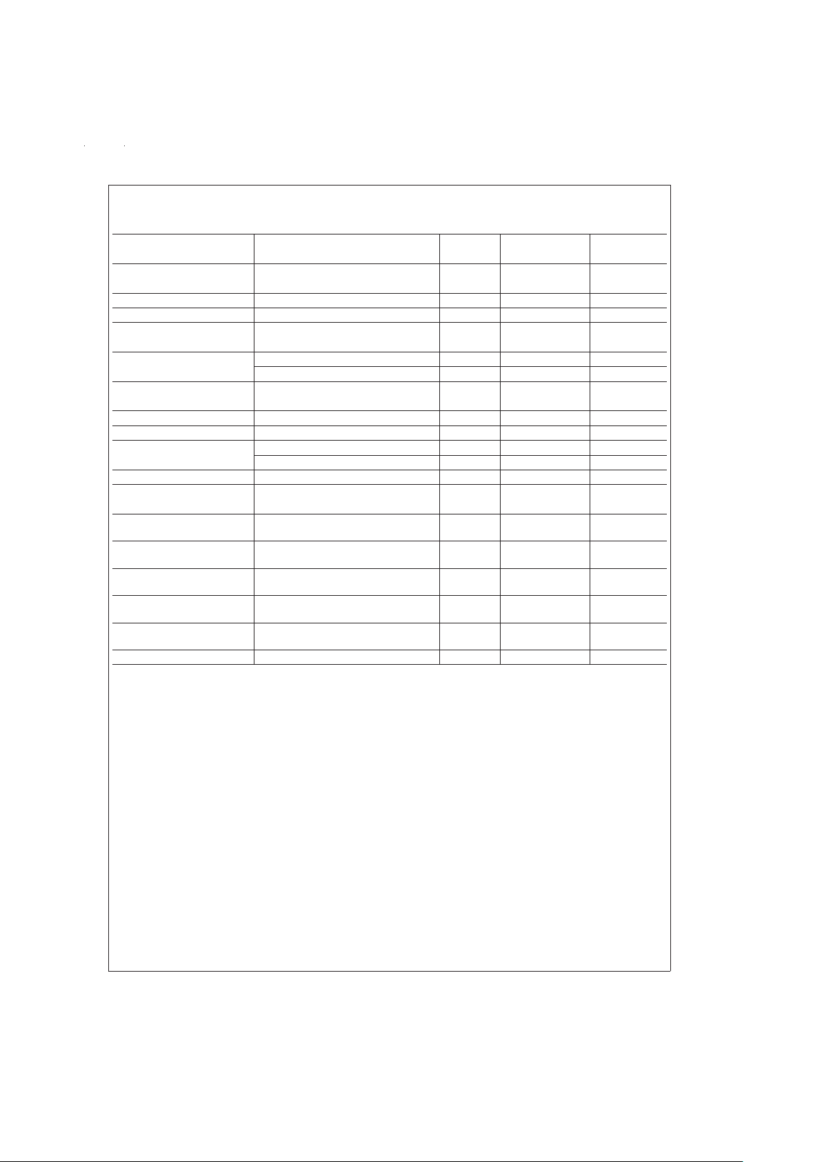
Electrical Characteristics—LM2941CT, LM2941CS
5V ≤ VO≤ 20V, V
IN
=
V
O
+ 5V, C
O
=
22 µF, unless otherwise specified. Specifications in standard typeface apply for T
J
=
25˚C, while those in boldface type apply over the full Operating Temperature Range.
Parameter Conditions Typ Limit Units
(Note 5) (Limits)
Reference Voltage 5 mA ≤ I
O
≤ 1A (Note 6) 1.275 1.237/1.211 V(min)
1.313/1.339 V(max)
Line Regulation V
O
+2V≤VIN≤ 26V, I
O
=
5 mA 4 10 mV/V(max)
Load Regulation 50 mA ≤ I
O
≤ 1A 7 10 mV/V(max)
Output Impedance 100 mADC and 20 mArms 7 mΩ/V
f
O
=
120 Hz
Quiescent Current V
O
+2V≤V
IN
<
26V, I
O
=
5 mA 10 15 mA(max)
V
IN
=
V
O
+ 5V, I
O
=
1A 30 45/60 mA(max)
RMS Output Noise, 10 Hz–100 kHz 0.003
%
%
of V
OUT
I
O
=
5mA
Ripple Rejection f
O
=
120 Hz, 1 Vrms, I
L
=
100 mA 0.005 0.02
%
/V(max)
Long Term Stability 0.4
%
/1000 Hr
Dropout Voltage I
O
=
1A 0.5 0.8/1.0 V(max)
I
O
=
100 mA 110 200/200 mV(max)
Short Circuit Current V
IN
max=26V (Note 7) 1.9 1.6 A(min)
Maximum Line V
O
max 1V above nominal V
O
55 45 V(min)
Transient R
O
=
100Ω,T≤100 ms
Maximum Operational Input
Voltage
31 26 V
DC
Reverse Polarity DC Input
Voltage
R
O
=
100Ω,V
O
≥−0.6V
−30 −15 V(min)
Reverse Polarity Transient
Input Voltage
T ≤ 100 ms, R
O
=
100Ω
−55 −45 V(min)
ON/OFF Threshold Voltage
ON
I
O
≤ 1A 1.30 0.80 V(max)
ON/OFF Threshold Voltage
OFF
I
O
≤ 1A 1.30 2.00 V(min)
ON/OFF Threshold Current V
ON/OFF
=
2.0V, I
O
≤ 1A 50 100 µA(max)
Note 1: AbsoluteMaximum Ratings indicate limits beyond which damage to the device may occur. Operating ratings indicate conditions for which the device is intended to be functional, but device parameter specifications may not be guaranteed under these conditions. For guaranteed specifications and test conditions, see
the Electrical Characteristics.
Note 2: A military RETS specification available upon request. For more information about military-aerospace products, see the Mil-Aero web page at
http://www.national.com/appinfo/milaero/index.html.
Note 3: Themaximum power dissipation is a function of T
J
(max), θJA, and TA. The maximum allowable power dissipation at any ambient temperature is P
D
=
(T
J
-
(max) − TA)/θJA. If this dissipation is exceeded, the die temperature will rise above 150˚C and the LM2941 will go into thermal shutdown. For the LM2941T and
LM2941CT,the junction-to-ambient thermal resistance (θ
JA
) is 53˚C/W, and the junction-to-case thermal resistance (θJC) is 3˚C/W. For the LM2941K, θJAis 35˚C/W
and θ
JC
is 4˚C/W.The junction-to-ambient thermal resistance of the TO-263 is 73˚C/W, and junction-to-case thermal resistance, θJCis 3˚C. If the TO-263 package
is used, the thermalresistance can be reduced by increasing the P.C. board copper areathermally connected to the package: Using 0.5square inches of copperarea,
θ
JA
is 50˚C/W; with 1 square inch of copper area, θJAis 37˚C/W; and with 1.6 or more square inches of copper area, θJAis 32˚C/W.
Note 4: Alllimits guaranteed at room temperature (standard typeface) and at temperature extremes (boldface type). All limits are used to calculate Outgoing Quality
Level, and are 100%production tested.
Note 5: Alllimitsguaranteed at room temperature (standard typeface) andat temperature extremes(boldface type). All room temperature limits are 100%production
tested. All limits at temperature extremes are guaranteed via correlation using standard Statistical Quality Control (SQC) methods.
Note 6: The output voltage range is 5V to 20V and is determined by the two external resistors, R1 and R2. See Typical Application Circuit.
Note 7: Output current capability will decrease with increasing temperature, but will not go below 1A at the maximum specified temperatures.
www.national.com3
Page 4

Typical Performance Characteristics
Dropout Voltage
DS008823-11
Dropout Voltage vs
Temperature
DS008823-12
Output Voltage
DS008823-13
Quiescent Current vs
Temperature
DS008823-14
Quiescent Current
DS008823-15
Quiescent Current
DS008823-16
Line Transient Response
DS008823-17
Load Transient Response
DS008823-18
Ripple Rejection
DS008823-19
Output Impedance
DS008823-20
www.national.com 4
Page 5

Typical Performance Characteristics (Continued)
Definition of Terms
Dropout Voltage: The input-voltage differential at which the
circuit ceases to regulate against further reduction in input
voltage. Measured when the output voltage has dropped
100 mV from the nominal value obtained at (V
OUT
+ 5V) input, dropout voltage is dependent upon load current and
junction temperature.
Input Voltage: The DC voltage applied to the input terminals
with respect to ground.
Input-Output Differential: The voltage difference between
the unregulated input voltage and the regulated output voltage for which the regulator will operate.
Line Regulation: The change in output voltage for a change
in the input voltage. The measurement is made under conditions of low dissipation or by using pulse techniques such
that the average chip temperature is not significantly affected.
Load Regulation: The change in output voltage for a
change in load current at constant chip temperature.
Long TermStability: Output voltage stability under accelerated life-test conditions after 1000 hours with maximum
rated voltage and junction temperature.
Output Noise Voltage: The rms AC voltage at the output,
with constant load and no input ripple, measured over a
specified frequency range.
Low Voltage Behavior
DS008823-21
Low Voltage Behavior
DS008823-22
Output Capacitor ESR
DS008823-23
Output at
Voltage Extremes
DS008823-24
Output at
Voltage Extremes
DS008823-25
Peak Output Current
DS008823-26
Maximum Power
Dissipation (TO-220)
DS008823-27
Maximum Power
Dissipation (TO-3)
DS008823-28
Maximum Power
Dissipation
(TO-263) (Note 3)
DS008823-29
www.national.com5
Page 6

Definition of Terms (Continued)
Quiescent Current: That part of the positive input current
that does not contribute to the positive load current. The
regulator ground lead current.
Ripple Rejection: The ratio of the peak-to-peak input ripple
voltage to the peak-to-peak output ripple voltage.
Temperature Stability of V
O
: The percentage change in
output voltage for a thermal variation from room temperature
to either temperature extreme.
Typical Applications
5V to 20V Adjustable Regulator
DS008823-3
Note: Using 1k for R1 will ensure that the input bias current error of the adjust pin will be negligible. Do not bypass R1 or R2. This will lead to instabilities.
* Required if regulator is located far from power supply filter.
*
*C
OUT
must be at least 22 µF to maintain stability. May be increased without bound to maintain regulation during transients. Locate as close as possible to the
regulator. This capacitor must be rated over the same operating temperature range as the regulator and the ESR is critical; see curve.
1A Switch
DS008823-6
**
* To assure shutdown, select Resistor R3 to guarantee at least 300 µA of pull-up current when S1 is open. (Assume 2V at the ON/OFF pin.)
www.national.com 6
Page 7

Equivalent Schematic Diagram
DS008823-1
www.national.com7
Page 8

Physical Dimensions inches (millimeters) unless otherwise noted
Order Number LM2941J/883
5962-9166701QEA
NS Package Number J16A
Order Number LM2941WG/883
5962-9166701QYA
NS Package Number WG16A
www.national.com 8
Page 9

Physical Dimensions inches (millimeters) unless otherwise noted (Continued)
Order Number LM2941T or LM2941CT
NS Package Number T05A
www.national.com9
Page 10

Physical Dimensions inches (millimeters) unless otherwise noted (Continued)
LIFE SUPPORT POLICY
NATIONAL’S PRODUCTS ARE NOT AUTHORIZED FOR USE AS CRITICAL COMPONENTS IN LIFE SUPPORT
DEVICES OR SYSTEMS WITHOUT THE EXPRESS WRITTEN APPROVAL OF THE PRESIDENT AND GENERAL
COUNSEL OF NATIONAL SEMICONDUCTOR CORPORATION. As used herein:
1. Life support devices or systems are devices or
systems which, (a) are intended for surgical implant
into the body, or (b) support or sustain life, and
whose failure to perform when properly used in
accordance with instructions for use provided in the
labeling, can be reasonably expected to result in a
significant injury to the user.
2. A critical component is any component of a life
support device or system whose failure to perform
can be reasonably expected to cause the failure of
the life support device or system, or to affect its
safety or effectiveness.
National Semiconductor
Corporation
Americas
Tel: 1-800-272-9959
Fax: 1-800-737-7018
Email: support@nsc.com
National Semiconductor
Europe
Fax: +49 (0) 1 80-530 85 86
Email: europe.support@nsc.com
Deutsch Tel: +49 (0) 1 80-530 85 85
English Tel: +49 (0) 1 80-532 78 32
Français Tel: +49 (0) 1 80-532 93 58
Italiano Tel: +49 (0) 1 80-534 16 80
National Semiconductor
Asia Pacific Customer
Response Group
Tel: 65-2544466
Fax: 65-2504466
Email: sea.support@nsc.com
National Semiconductor
Japan Ltd.
Tel: 81-3-5639-7560
Fax: 81-3-5639-7507
www.national.com
TO-263 5-Lead Plastic Surface Mount Package
Order Number LM2941S or LM2941CS
NS Package Number TS5B
LM2941/LM2941C 1A Low Dropout Adjustable Regulator
National does not assume any responsibility for use of any circuitry described, no circuit patent licenses are implied and National reserves the right at any time without notice to change said circuitry and specifications.
 Loading...