

Page 1
Order this document by LM2935/D
SEMICONDUCTOR
TECHNICAL DATA
LOW DROPOUT
DUAL VOLTAGE REGULATOR
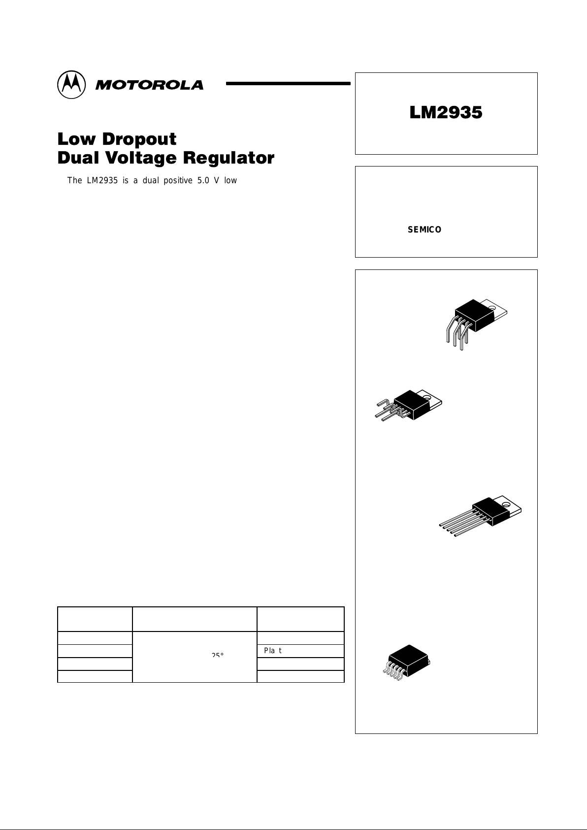
1
5
TV SUFFIX
PLASTIC PACKAGE
CASE 314B
T SUFFIX
PLASTIC PACKAGE
CASE 314D
TH SUFFIX
PLASTIC PACKAGE
CASE 314A
Heatsink surface connected to Pin 3.
5
1
D2T SUFFIX
PLASTIC PACKAGE
CASE 936A
(D2PAK)
Pin 1. Input Voltage/V
CC
2. Main Output
3. Ground
4. Switch/Reset
5. Standby/Output
Heatsink surface (shown as terminal 6
in case outline drawing) is connected to Pin 3.
5
1
5
1
1
MOTOROLA ANALOG IC DEVICE DATA
The LM2935 is a dual positive 5.0 V low dropout voltage regulator,
designed for standby power systems. The main output is capable of
supplying 750 mA for microprocessor power, and can be turned “on” and
“off” by the switch/reset input. The other output is dedicated for standby
operation of volatile memory , and is capable of supplying up to 10 mA loads.
The total device features a low quiescent current of 3.0 mA or less when
supplying 10 mA from the standby output.
This part was designed for harsh automotive environments and is
therefore immune to many input supply voltage problems such as reverse
battery (–12 V), double battery (+24 V), and load dump transients (+60 V).
• Two Regulated 5.0 V Outputs
• Main Output Current in Excess of 750 mA
• On/Off Control of Main Output
• Standby Output Current in Excess of 10 mA
• Low Input/Output Differential of Less than 0.6 V at 500 mA
• Short Circuit Current Limiting
• Internal Thermal Shutdown
• Low Voltage Indicator Output
• Designed for Automotive Environment Including
• Reverse Battery Protection
• Double Battery Protection
• Load Dump Protection
• Reverse Transient Protection
• Economical 5–Lead TO–220 Package with Two Optional Leadforms
• Also Available in Surface Mount D
2
PAK Package
ORDERING INFORMATION
Device
Operating
Temperature Range
Package
LM2935D2T
Surface Mount
LM2935T
–
°
°
Plastic Power
LM2935TH
T
J
= –
40° to +125°C
Horizontal Mount
LM2935TV Vertical Mount
Motorola, Inc. 1996 Rev 1
Page 2
LM2935
2
MOTOROLA ANALOG IC DEVICE DATA
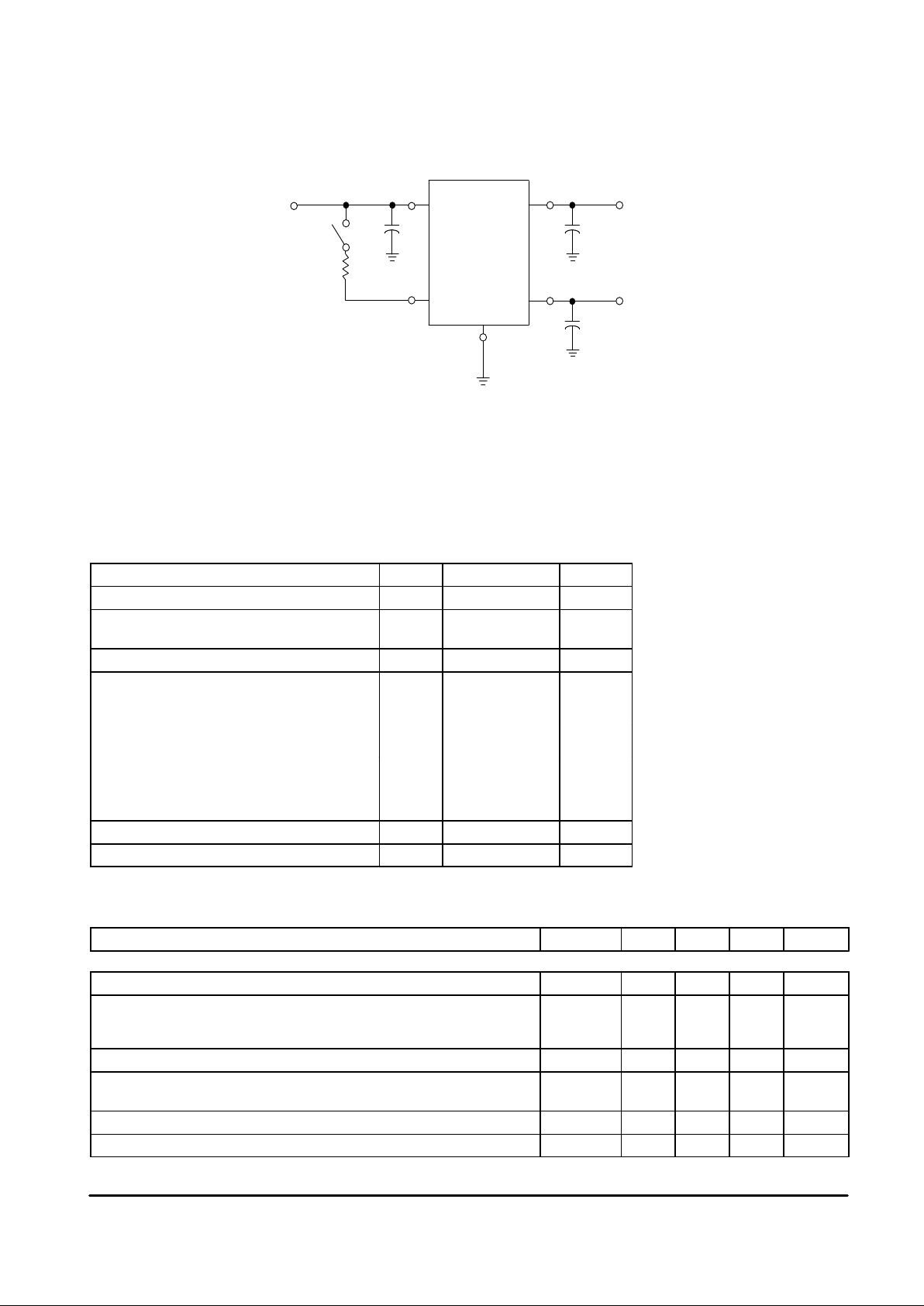
*The main output
is “Off” with switch
S1 open.
An input bypass capacitor is recommended if the regulator is located more than 4
″
from the supply
input filter. The LM2935 is not internally compensated and thus requires an external output capacitor
for stability. A minimum capacitance of 10
µ
F is recommended. The actual capacitance value is
dependent upon load current, temperature, and the capacitor’s equivalent series resistance (ESR).
The least stable condition is encountered at maximum load current and minimum ambient
temperature.
V
in
S1*
0.1
Input
Switch/
Reset
Gnd
3
1
4
Standby
Main
Output
2
20 k
LM2935
5.0 V/750 mA
+
10
Typical Application Circuit
This device contains 29 active transistors.
5
5.0 V/10 mA
+
10
MAXIMUM RATINGS
Rating Symbol Value Unit
Input Voltage Continuous V
I
60 Vdc
Transient Reverse Polarity Input V oltage
1.0% Duty Cycle, τ ≤ 100 ms
–VI(τ) –50 Vpk
Switch/Reset Input Current I
in
5.0 mA
Power Dissipation
Case 314A, 314B and 314D (TO–220 Type)
TA = 25°C P
D
Internally Limited W
Thermal Resistance, Junction–to–Ambient R
θJA
65 °C/W
Thermal Resistance, Junction–to–Case R
θJC
5.0 °C/W
Case 936A (D2PAK)
TA = 25°C P
D
Internally Limited W
Thermal Resistance, Junction–to–Ambient R
θJA
Per Figure 1 °C/W
Thermal Resistance, Junction–to–Case R
θJC
5.0 °C/W
Operating Junction Temperature Range T
J
–40 to +150 °C
Storage Temperature Range T
stg
–65 to +150 °C
ELECTRICAL CHARACTERISTICS (V
in
= 14 V, IO = 500 mA, I
stby
= 0 mA, CO = 10 µF, C
stby
= 10 µF, TJ = 25°C [Note 1].)
Characteristic Symbol Min Typ Max Unit
MAIN OUTPUT
Output Voltage (Vin = 6.0 V to 26 V, IO= 5.0 mA to 500 mA, TJ = –40 to +125°C) V
O
4.75 5.0 5.25 V
Line Regulation
Vin = 9.0 V to 16 V, IO= 5.0 mA
Vin = 6.0 V to 26 V, IO= 5.0 mA
Reg
line
–
–
4.0
10
25
50
mV
Load Regulation (IO = 5.0 mA to 500 mA) Reg
load
– 10 50 mV
Output Impedance
IO = 500 mAdc and 10 mArms, f = 100 Hz to 10 kHz
Z
O
– 200 –
mΩ
Output Noise Voltage (f = 10 Hz to 100 kHz) V
n
– 100 – µVrms
Long Term Stability S – 20 – mV/kHR
Page 3
LM2935
3
MOTOROLA ANALOG IC DEVICE DATA
ELECTRICAL CHARACTERISTICS (V
in
= 14 V, IO = 500 mA, I
stby
= 0 mA, CO = 10 µF, C
stby
= 10 µF, TJ = 25°C [Note 1].)
Characteristic UnitMaxTypMinSymbol
MAIN OUTPUT (continued)
Ripple Rejection (f = 120 Hz) RR – 66 – dB
Dropout Voltage
IO = 500 mA
IO = 750 mA
VI–V
O
–
–
0.45
0.82
0.6
–
V
Short Circuit Current Limit I
SC
0.75 1.2 – A
Over–Voltage Shutdown Threshold V
th(OV)
26 31 – V
SWITCH/RESET
Output Sink Current (VOL = 1.2 V) I
Sink
– 5.0 – mA
Output Voltage (R
on/off
= 20 kΩ)
Low State, Vin = 4.0 V
High State, Vin = 14 V
V
OL
V
OH
–
4.5
0.9
5.0
1.2
6.0
V
Output Pull–Up Resistor, “On”/“Off” (Note 2) R
on/off
– 20 30 kΩ
Output Voltage with Reverse Polarity Input (Vin = –15 V, RL = 10 Ω) –V
O
–0.6 0 – V
ELECTRICAL CHARACTERISTICS (V
in
= 14 V, IO = 0 mA, I
stby
= 10 mA, CO = 10 µF, C
stby
= 10 µF, TJ = 25°C [Note 1].)
Characteristic
Symbol Min Typ Max Unit
STANDBY OUTPUT
Output Voltage (Vin = 6.0 V to 26 V, I
stby
= 1.0 mA to 10 mA, TJ = –40 to +125°C) V
O(stby)
4.75 5.0 5.25 V
Tracking Voltage VO–V
O(stby)
–200 0 200 mV
Line Regulation (Vin = 6.0 V to 26 V) Reg
line
– 4.0 50 mV
Load Regulation (I
stby
= 1.0 mA to 10 mA) Reg
load
– 10 50 mV
Output Impedance
I
(stby)
= 10 mAdc and 1.0 mArms, f = 100 Hz to 10 kHz
Z
O(stby)
– 1.0 –
Ω
Output Noise Voltage (f = 10 Hz to 100 kHz) V
n
– 300 – µV rms
Long Term Stability S – 20 – mV/kHR
Ripple Rejection (f = 120 Hz) RR – 66 – dB
Dropout Voltage (I
stby
= 10 mA) VI–V
O(stby)
– 0.55 0.7 V
Short Circuit Current Limit I
SC
25 70 – mA
Output Voltage with Reverse Polarity Input
Vin = –15 V, RL = 510 Ω
–V
O
–0.3 0 –
V
Output Voltage with Maximum Positive Input
Vin = 60 V, RL = 510 Ω
V
O(max)
– 5.0 6.0
V
TOTAL DEVICE
Bias Current
IO = 10 mA, I
stby
= 0 mA
IO = 500 mA, I
stby
= 0 mA
IO = 750 mA, I
stby
= 0 mA
Main Output “Off”, I
stby
= 10 mA
I
B
–
–
–
–
3.0
40
90
2.0
–
100
–
3.0
mA
NOTES: 1.Low duty cycle pulse techniques are used during test to maintain junction temperature as close to ambient as possible.
2.The maximum switch/reset current must not exceed 5.0 mA.
Page 4

LM2935
4
MOTOROLA ANALOG IC DEVICE DATA
Vin, Input Voltage
(Pin 1)
S1, “On”/“Off” Switch
VO, Main Output Voltage
(Pin 2)
Reset (Pin 4)
V
stby
, Standby Voltage
(Pin 5)
Open
Main
Output
Turn “On”
Load
Dump
Low Input
Voltage
Input
Voltage
Line Noise
Main
Output
Short
Circuit
Thermal
Shutdown
Main
Output
Turn “Off”
Open
Closed
60 V
14 V
3.0 V
5.0 V
2.4 V
0 V
9.0 V
14 V
14 V
5.0 V 5.0 V 5.0 V 5.0 V
5.0 V
5.0 V 5.0 V
0 V
2.4 V
26 V
TYPICAL CIRCUIT WAVEFORMS
R , THERMAL RESISTANCE
JA
θ
JUNCTION–TO–AIR ( C/W)
°
30
40
50
60
70
80
1.0
1.5
2.0
2.5
3.0
3.5
010203025155.0
L, LENGTH OF COPPER (mm)
P
D(max)
for TA = 50°C
Minimum
Size Pad
2.0 oz. Copper
L
L
Free Air
Mounted
Vertically
P
D
, MAXIMUM POWER DISSIPATION (W)
R
θ
JA
Figure 1. D2PAK Thermal Resistance and Maximum
Power Dissipation versus P.C.B. Copper Length
Page 5

LM2935
5
MOTOROLA ANALOG IC DEVICE DATA
TH SUFFIX
PLASTIC PACKAGE
CASE 314A–03
ISSUE D
OUTLINE DIMENSIONS
TV SUFFIX
PLASTIC PACKAGE
CASE 314B–05
ISSUE J
G
W
E
J 5 PL
D 5 PL
F
K
U
B
A
L
C
H
12345
NOTES:
1. DIMENSIONING AND TOLERANCING PER ANSI
Y14.5M, 1982.
2. CONTROLLING DIMENSION: INCH.
3. DIMENSION D DOES NOT INCLUDE
INTERCONNECT BAR (DAMBAR) PROTRUSION.
DIMENSION D INCLUDING PROTRUSION SHALL
NOT EXCEED 0.043 (1.092) MAXIMUM.
1.702 BSC0.067 BSC
MIN MINMAX MAX
INCHES MILLIMETERS
DIM
A
B
C
D
E
F
G
H
J
K
L
N
Q
S
U
V
W
14.529
9.906
4.318
0.635
1.219
21.590
0.381
22.860
8.128
3.556
–
11.888
–
2.286
15.570
10.541
4.572
0.965
1.397
23.749
0.635
27.940
9.271
3.886
15.748
12.827
18.669
2.794
0.572
0.390
0.170
0.025
0.048
0.850
0.015
0.900
0.320
0.140
–
0.468
–
0.090
0.613
0.415
0.180
0.038
0.055
0.935
0.025
1.100
0.365
0.153
0.620
0.505
0.735
0.110
SEATING
PLANE
–T–
N
S
V
T
0.24 (0.610)
M
–P–
Q
TP0.10 (0.254)
M M
4.216 BSC0.166 BSC
8.128 BSC0.320 BSC
OPTIONAL
CHAMFER
G
E
J 5 PL
D 5 PL
F
K
U
B
A
L
C
12345
NOTES:
1. DIMENSIONING AND TOLERANCING PER ANSI
Y14.5M, 1982.
2. CONTROLLING DIMENSION: INCH.
3. DIMENSION D DOES NOT INCLUDE
INTERCONNECT BAR (DAMBAR) PROTRUSION.
DIMENSION D INCLUDING PROTRUSION SHALL
NOT EXCEED 0.043 (1.092) MAXIMUM.
SEATING
PLANE
–T–
S
TP0.014 (0.356)
M M
OPTIONAL
CHAMFER
Q
DIMAMIN MAX MIN MAX
MILLIMETERS
0.572 0.613 14.529 15.570
INCHES
B 0.390 0.415 9.906 10.541
C 0.170 0.180 4.318 4.572
D 0.025 0.038 0.635 0.965
E 0.048 0.055 1.219 1.397
F 0.570 0.585 14.478 14.859
G 0.067 BSC 1.702 BSC
J 0.015 0.025 0.381 0.635
K 0.730 0.745 18.542 18.923
L 0.320 0.365 8.128 9.271
Q 0.140 0.153 3.556 3.886
S 0.210 0.260 5.334 6.604
U 0.468 0.505 11.888 12.827
–P–
Page 6

LM2935
6
MOTOROLA ANALOG IC DEVICE DATA
T SUFFIX
PLASTIC PACKAGE
CASE 314D–03
ISSUE D
OUTLINE DIMENSIONS
D2T SUFFIX
PLASTIC PACKAGE
CASE 936A–02
(D2PAK)
ISSUE A
–Q–
–T–
SEATING
PLANE
C
U
G
E
H
J
NOTES:
1. DIMENSIONING AND TOLERANCING PER ANSI
Y14.5M, 1982.
2. CONTROLLING DIMENSION: INCH.
3. DIMENSION D DOES NOT INCLUDE
INTERCONNECT BAR (DAMBAR) PROTRUSION.
DIMENSION D INCLUDING PROTRUSION SHALL
NOT EXCEED 10.92 (0.043) MAXIMUM.
MIN MINMAX MAX
INCHES MILLIMETERS
DIM
A
B
C
D
E
G
H
J
K
L
Q
U
S
14.529
9.906
4.318
0.635
1.219
2.210
0.381
25.908
8.128
3.556
2.667
13.792
15.570
10.541
4.572
0.965
1.397
2.845
0.635
27.051
9.271
3.886
2.972
14.783
0.572
0.390
0.170
0.025
0.048
0.087
0.015
1.020
0.320
0.140
0.105
0.543
0.613
0.415
0.180
0.038
0.055
0.112
0.025
1.065
0.365
0.153
0.117
0.582
A
B
L
S
K
D
5 PL
1.702 BSC0.067 BSC
1234 5
0.356 (0.014) T Q
M M
5 REF
A
123
K
B
S
H
0.010 (0.254) T
M
D
G
C
E
–T–
M
L
P
N
R
V
U
TERMINAL 6
NOTES:
1 DIMENSIONING AND TOLERANCING PER ANSI
Y14.5M, 1982.
2 CONTROLLING DIMENSION: INCH.
3 TAB CONTOUR OPTIONAL WITHIN DIMENSIONS
A AND K.
4 DIMENSIONS U AND V ESTABLISH A MINIMUM
MOUNTING SURFACE FOR TERMINAL 6.
5 DIMENSIONS A AND B DO NOT INCLUDE MOLD
FLASH OR GATE PROTRUSIONS. MOLD FLASH
AND GATE PROTRUSIONS NOT TO EXCEED
0.025 (0.635) MAXIMUM.
DIMAMIN MAX MIN MAX
MILLIMETERS
0.386 0.403 9.804 10.236
INCHES
B 0.356 0.368 9.042 9.347
C 0.170 0.180 4.318 4.572
D 0.026 0.036 0.660 0.914
E 0.045 0.055 1.143 1.397
G 0.067 BSC 1.702 BSC
H 0.539 0.579 13.691 14.707
K 0.050 REF 1.270 REF
L 0.000 0.010 0.000 0.254
M 0.088 0.102 2.235 2.591
N 0.018 0.026 0.457 0.660
P 0.058 0.078 1.473 1.981
R 5 REF
S 0.116 REF 2.946 REF
U 0.200 MIN 5.080 MIN
V 0.250 MIN 6.350 MIN
__
45
OPTIONAL
CHAMFER
Page 7

LM2935
7
MOTOROLA ANALOG IC DEVICE DATA
Motorola reserves the right to make changes without further notice to any products herein. Motorola makes no warranty , representation or guarantee regarding
the suitability of its products for any particular purpose, nor does Motorola assume any liability arising out of the application or use of any product or circuit, and
specifically disclaims any and all liability, including without limitation consequential or incidental damages. “T ypical” parameters which may be provided in Motorola
data sheets and/or specifications can and do vary in different applications and actual performance may vary over time. All operating parameters, including “Typicals”
must be validated for each customer application by customer’s technical experts. Motorola does not convey any license under its patent rights nor the rights of
others. Motorola products are not designed, intended, or authorized for use as components in systems intended for surgical implant into the body, or other
applications intended to support or sustain life, or for any other application in which the failure of the Motorola product could create a situation where personal injury
or death may occur. Should Buyer purchase or use Motorola products for any such unintended or unauthorized application, Buyer shall indemnify and hold Motorola
and its officers, employees, subsidiaries, affiliates, and distributors harmless against all claims, costs, damages, and expenses, and reasonable attorney fees
arising out of, directly or indirectly, any claim of personal injury or death associated with such unintended or unauthorized use, even if such claim alleges that
Motorola was negligent regarding the design or manufacture of the part. Motorola and are registered trademarks of Motorola, Inc. Motorola, Inc. is an Equal
Opportunity/Affirmative Action Employer.
Page 8

LM2935
8
MOTOROLA ANALOG IC DEVICE DATA
How to reach us:
USA/EUROPE/Locations Not Listed: Motorola Literature Distribution; JAP AN: Nippon Motorola Ltd.; Tatsumi–SPD–JLDC, 6F Seibu–Butsuryu–Center,
P.O. Box 20912; Phoenix, Arizona 85036. 1–800–441–2447 or 602–303–5454 3–14–2 Ta tsumi Koto–Ku, Tokyo 135, Japan. 03–81–3521–8315
MFAX: RMF AX0@email.sps.mot.com – TOUCHT ONE 602–244–6609 ASIA/PACIFIC: Motorola Semiconductors H.K. Ltd.; 8B Tai Ping Industrial Park,
INTERNET: http://Design–NET.com 51 Ting Ko k Road, Tai Po, N.T ., Hong Kong. 852–26629298
LM2935/D
*LM2935/D*
◊
 Loading...