

Page 1
LM2931
Series Low Dropout Regulators
General Description
The LM2931 positive voltage regulator features a very low
quiescent current of 1mA or less when supplying 10mA
loads. This unique characteristic and the extremely low
input-output differential required for proper regulation (0.2V
for output currents of 10mA) make the LM2931 the ideal
regulator for standby power systems. Applications include
memory standby circuits, CMOS and other low power processor power supplies as well as systems demanding as
much as 100mA of output current.
Designed originally for automotive applications, the LM2931
and all regulated circuitry are protected from reverse battery
installations or 2 battery jumps. During line transients, such
as a load dump (60V) when the input voltage to the regulator
can momentarily exceed the specified maximum operating
voltage, the regulator will automatically shut down to protect
both internal circuits and the load. The LM2931 cannot be
harmed by temporary mirror-image insertion. Familiar regulator features such as short circuit and thermal overload protection are also provided.
The LM2931 family includes a fixed 5V output (
±
3.8% toler-
ance for A grade) or an adjustable output with ON/OFF pin.
Both versions are available in a TO-220 power package,
TO-263 surface mount package, and an 8-lead surface
mount package. The fixed output version is also available in
the TO-92 plastic and 6-Bump micro SMD packages.
Features
n Very low quiescent current
n Output current in excess of 100 mA
n Input-output differential less than 0.6V
n Reverse battery protection
n 60V load dump protection
n −50V reverse transient protection
n Short circuit protection
n Internal thermal overload protection
n Mirror-image insertion protection
n Available in TO-220, TO-92, TO-263, SO-8 or 6-Bump
micro SMD packages
n Available as adjustable with TTL compatible switch
n See AN-1112 for micro SMD considerations
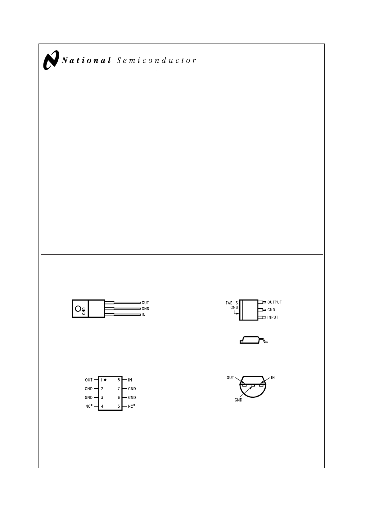
Connection Diagrams
FIXED VOLTAGE OUTPUT
TO-220 3-Lead Power Package
DS005254-6
Front View
TO-263 Surface-Mount Package
DS005254-11
Top View
DS005254-12
Side View
8-Pin Surface Mount
DS005254-7
*NC = Not internally connected. Must be electrically isolated from the rest
of the circuit for the micro SMD package.
Top View
TO-92 Plastic Package
DS005254-8
Bottom View
March 2000
LM2931Series Low Dropout Regulators
© 2000 National Semiconductor Corporation DS005254 www.national.com
Page 2
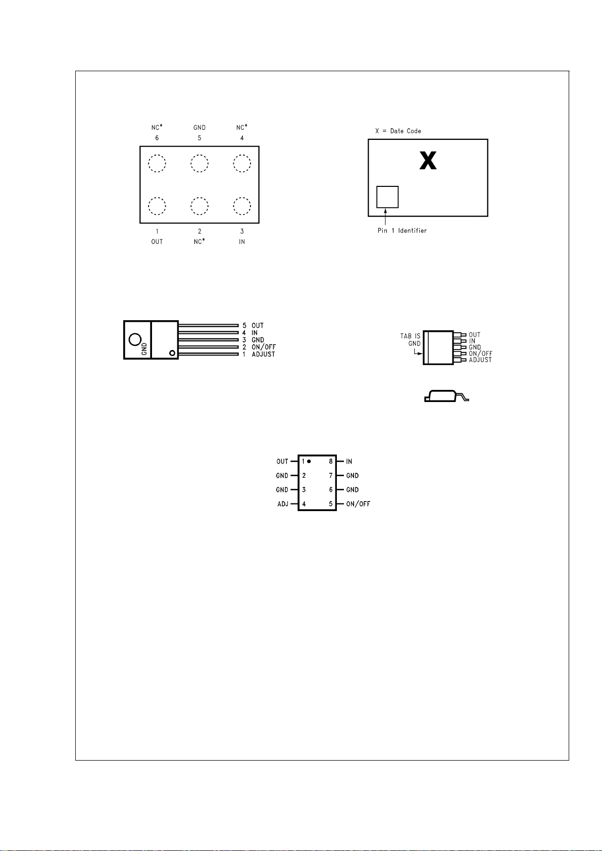
Connection Diagrams (Continued)
ADJUSTABLE OUTPUT VOLTAGE
6-Bump micro SMD
DS005254-38
Top View
(Bump Side Down)
micro SMD Laser Mark
DS005254-39
TO-220 5-Lead Power Package
DS005254-9
Front View
TO-263
5-Lead Surface-Mount Package
DS005254-13
Top View
DS005254-14
Side View
8-Pin Surface Mount
DS005254-10
Top View
LM2931
www.national.com 2
Page 3
Connection Diagrams (Continued)
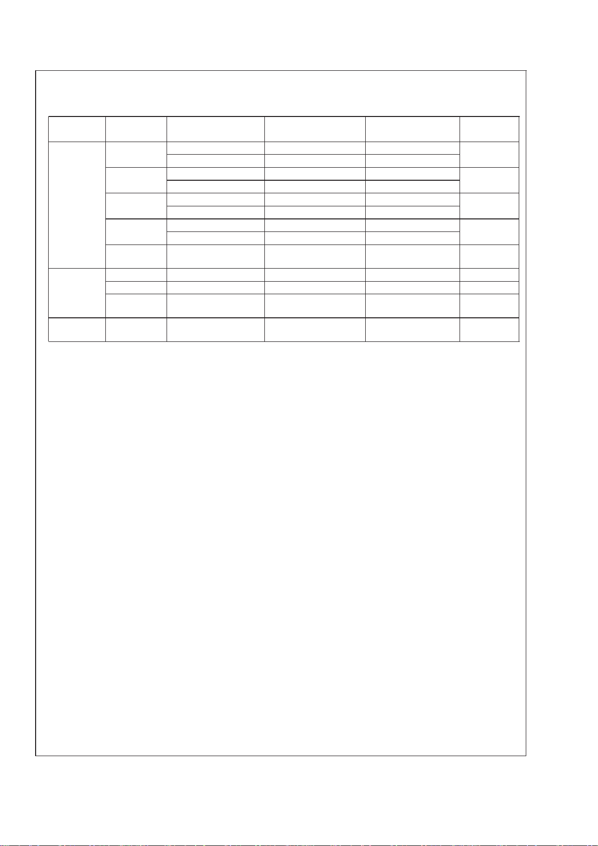
Ordering Information
Output
Number
Package Part Number Package Marking Transport Media NSC
Drawing
5V 3-Pin TO-220 LM2931T-5.0 LM2931T-5.0 Rails T03B
LM2931AT-5.0 LM2931AT-5.0 Rails
3-Pin TO-263 LM2931S-5.0 LM2931S-5.0 Rails TS3B
LM2931AS-5.0 LM2931AS-5.0 Rails
TO-92 LM2931Z-5.0 LM2931Z-5 1.8k Units per Box Z03A
LM2931AZ-5.0 LM2931AZ 1.8k Units per Box
8-Pin
SOIC
LM2931M-5.0 2931M-5.0 Rails M08A
LM2931AM-5.0 2931AM-5.0 Rails
*
6-Bump
micro SMD
LM2931IBPX-5.0 - Tape and Reel BPA06HTA
Adjustable,
3V to 24V
5-Pin TO-220 LM2931CT LM2931CT Rails T05A
5-Pin TO-263 LM2931CS LM2931CS Rails TS5B
8-Pin
SOIC
LM2931CM LM2931CM Rails M08A
3.3V
*
6-Bump
micro SMD
LM2931IBPX-3.3 - Tape and Reel BPA06HTA
Note: The micro SMD package marking is a single digit manufacturing Date Code Only.
LM2931
www.national.com3
Page 4
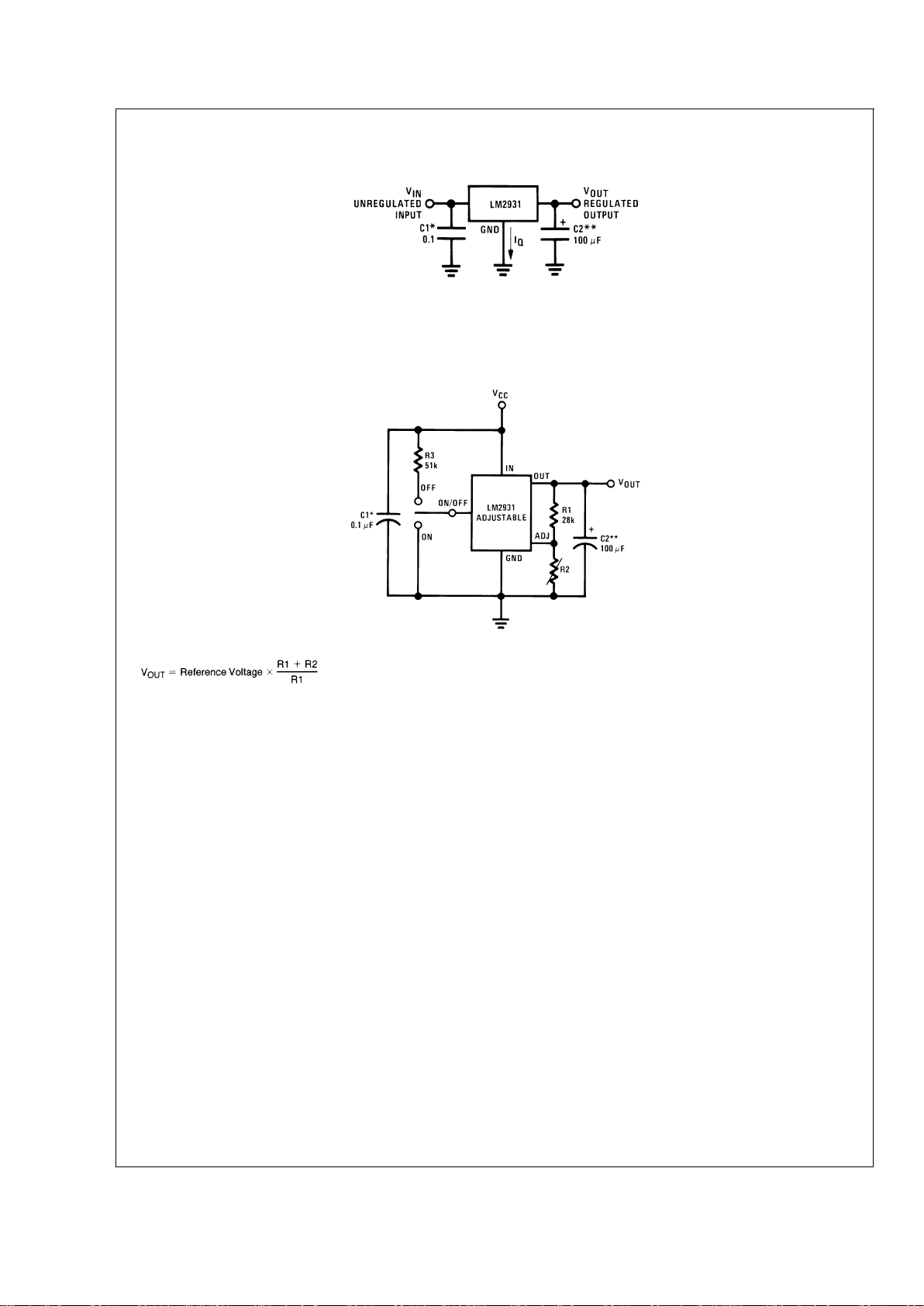
Typical Applications
LM2931 Fixed Output
DS005254-4
*
Required if regulator is located far from power supply filter.
*
*C2 must be at least 100 µF to maintain stability. May be increased without bound to maintain regulation during transients. Locate as close as possible to the
regulator. This capacitor must be rated over the same operating temperature range as the regulator. The equivalent series resistance (ESR) of this capacitor is
critical; see curve.
LM2931 Adjustable Output
DS005254-5
Note: Using 27k for R1 will automatically compensate for errors in V
OUT
due to the input bias current of the ADJ pin (approximately 1 µA).
LM2931
www.national.com 4
Page 5
Absolute Maximum Ratings (Note 1)
If Military/Aerospace specified devices are required,
please contact the National Semiconductor Sales Office/
Distributors for availability and specifications.
Input Voltage
Operating Range 26V
Overvoltage Protection
LM2931A, LM2931C (Adjustable) 60V
LM2931 50V
Internal Power Dissipation
(Note 2) (Note 4) Internally Limited
Operating Ambient Temperature
Range −40˚C to +85˚C
Maximum Junction Temperature 125˚C
Storage Temperature Range −65˚C to +150˚C
Lead Temp. (Soldering, 10 seconds) 230˚C
ESD Tolerance (Note 5) 2000V
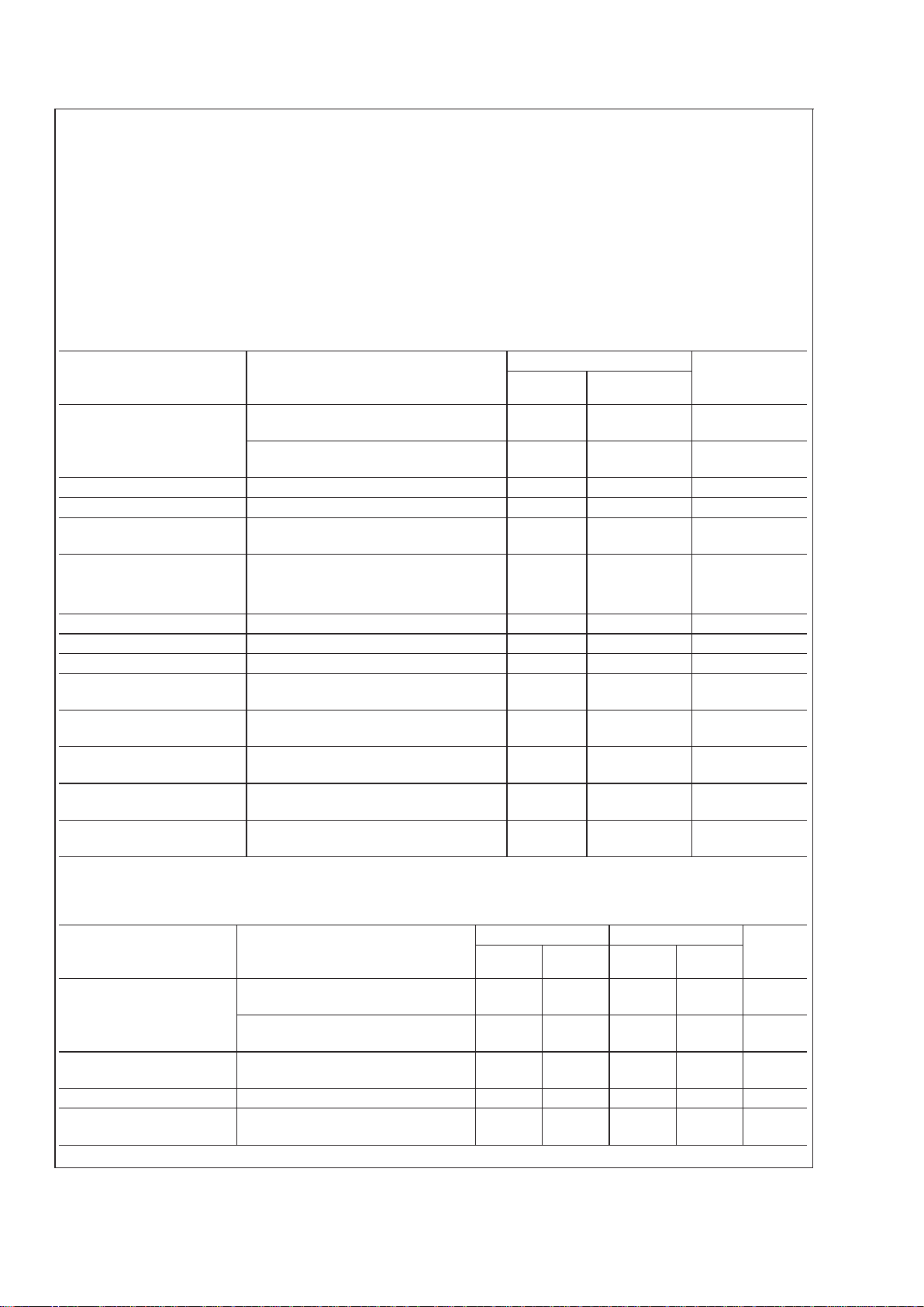
Electrical Characteristics for Fixed 3.3V Version
VIN= 14V, IO= 10mA, TJ= 25˚C, C2= 100µF (unless otherwise specified) (Note 2)
Parameter Conditions LM2931-3.3 Units
Typ Limit
(Note 3)
Output Voltage 3.3 3.465
3.135
V
MAX
V
MIN
4V ≤ VIN≤ 26V, IO= 100 mA
−40˚C ≤ T
J
≤ 125˚C
3.630
2.970
V
MAX
V
MIN
Line Regulation 4V ≤ VIN≤ 26V 4 33 mV
MAX
Load Regulation 5mA ≤ IO≤ 100mA 10 50 mV
MAX
Output Impedance 100mADCand 10mA
rms
,
100Hz - 10kHz
200 mΩ
Quiescent Current I
O
≤ 10mA, 4V ≤ VIN≤ 26V 0.4 1.0 mA
MAX
−40˚C ≤ TJ≤ 125˚C
I
O
= 100mA, VIN= 14V, TJ= 25˚C 15 mA
Output Noise Voltage 10Hz -100kHz, C
OUT
= 100µF 330 µV
rms
Long Term Stability 13 mV/1000 hr
Ripple Rejection f
O
= 120Hz 80 dB
Dropout Voltage I
O
= 10mA
I
O
= 100mA
0.05
0.30
0.2
0.6
V
MAX
Maximum Operational
Input Voltage
33 26 V
MIN
Maximum Line Transient RL= 500Ω,VO≤5.5V,
T = 1ms, τ≤100ms
70 50 V
MIN
Reverse Polarity Input
Voltage, DC
VO≥ −0.3V, RL= 500Ω −30 −15 V
MIN
Reverse Polarity Input
Voltage, Transient
T = 1ms, τ≤100ms, RL= 500Ω −80 −50 V
MIN
Electrical Characteristics for Fixed 5V Version
VIN= 14V, IO= 10mA, TJ= 25˚C, C2 = 100 µF (unless otherwise specified) (Note 2)
Parameter Conditions LM2931A-5.0 LM2931-5.0 Units
Typ
Limit
(Note 3)
Typ
Limit
(Note 3)
Output Voltage 5 5.19
4.81
5 5.25
4.75
V
MAX
V
MIN
6.0V ≤ VIN≤ 26V, IO= 100mA
−40˚C ≤ T
J
≤ 125˚C
5.25
4.75
5.5
4.5
V
MAX
V
MIN
Line Regulation 9V ≤ VIN≤ 16V
6V ≤ V
IN
≤ 26V
2
4
10
30
2
4
10
30
mV
MAX
Load Regulation 5 mA ≤ IO≤ 100mA 14 50 14 50 mV
MAX
Output Impedance 100mADCand 10mA
rms
,
100Hz -10kHz
200 200 mΩ
LM2931
www.national.com5
Page 6
Electrical Characteristics for Fixed 5V Version (Continued)
VIN= 14V, IO= 10mA, TJ= 25˚C, C2 = 100 µF (unless otherwise specified) (Note 2)
Parameter Conditions LM2931A-5.0 LM2931-5.0 Units
Typ
Limit
(Note 3)
Typ
Limit
(Note 3)
Quiescent Current I
O
≤ 10mA, 6V ≤ VIN≤ 26V 0.4 1.0 0.4 1.0 mA
MAX
−40˚C ≤ TJ≤ 125˚C
I
O
= 100mA, VIN= 14V, TJ= 25˚C 15 30
5
15 mA
MAX
mA
MIN
Output Noise Voltage 10Hz -100kHz, C
OUT
= 100µF 500 500 µV
rms
Long Term Stability 20 20 mV/1000
hr
Ripple Rejection f
O
= 120 Hz 80 55 80 dB
MIN
Dropout Voltage IO= 10mA
I
O
= 100mA
0.05
0.3
0.2
0.6
0.05
0.3
0.2
0.6
V
MAX
Maximum Operational Input
Voltage
33 26 33 26 V
MIN
Maximum Line Transient RL= 500Ω,VO≤5.5V,
T = 1ms, τ≤100ms
70 60 70 50 V
MIN
Reverse Polarity Input
Voltage, DC
VO≥ −0.3V, RL= 500Ω −30 −15 −30 −15 V
MIN
Reverse Polarity Input
Voltage, Transient
T = 1ms, τ≤100ms, RL= 500Ω −80 −50 −80 −50 V
MIN
Note 1: Absolute Maximum Ratings indicate limits beyond which damage to the device may occur. Electrical specifications do not apply when operating the device
beyond its rated operating conditions.
Note 2: See circuit in Typical Applications. To ensure constant junction temperature, low duty cycle pulse testing is used.
Note 3: All limits are guaranteed for T
J
= 25˚C (standard type face) or over the full operating junction temperature range of −40˚C to +125˚C (bold type face).
Note 4: The maximum power dissipation is a function of maximum junction temperatureT
Jmax
, total thermal resistance θJA, and ambient temperature TA. The maxi-
mum allowable power dissipation at any ambient temperature is P
D
=(T
Jmax−TA
)/θJA. If this dissipation is exceeded, the die temperature will rise above150˚Cand
the LM2931 will gointothermalshutdown. For the LM2931 in the TO-92 package, θ
JA
is 195˚C/W; in the SO-8 package, θJAis 160˚C/W, and in the TO-220 package,
θ
JA
is 50˚C/W; in the TO-263 package, θJAis 73˚C/W; and in the 6-Bump micro SMD package θJAis 290˚C/W. If the TO-220 package is used with a heat sink, θ
JA
is the sum of the package thermal resistance junction-to-case of 3˚C/W and the thermal resistance added by the heat sink and thermal interface.
If the TO-263 package is used, the thermal resistance can be reduced by increasing the P.C. board copper area thermally connected to the package: Using 0.5 square
inches of copper area, θ
JA
is 50˚C/W; with 1 square inch of copper area, θJAis 37˚C/W; and with 1.6 or more square inches of copper area, θJAis 32˚C/W.
Note 5: Human body model, 100 pF discharged through 1.5 kΩ.
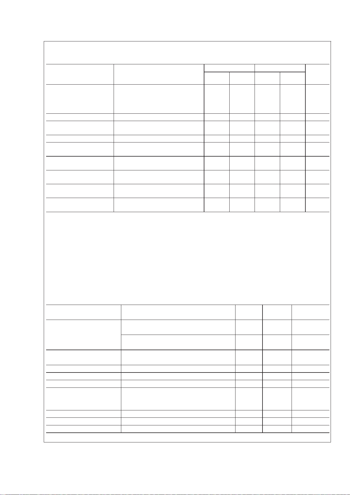
Electrical Characteristics for Adjustable Version
VIN= 14V, V
OUT
= 3V, IO= 10 mA, TJ= 25˚C, R1 = 27k, C2 = 100 µF (unless otherwise specified) (Note 2)
Parameter Conditions Typ Limit Units
Limit
Reference Voltage 1.20 1.26 V
MAX
1.14 V
MIN
IO≤ 100 mA, −40˚C ≤ Tj≤ 125˚C, R1 = 27k 1.32 V
MAX
Measured from V
OUT
to Adjust Pin 1.08 V
MIN
Output Voltage Range 24 V
MAX
3V
MIN
Line Regulation V
OUT
+ 0.6V ≤ VIN≤ 26V 0.2 1.5 mV/V
MAX
Load Regulation 5 mA ≤ IO≤ 100 mA 0.3 1 %
MAX
Output Impedance 100 mADCand 10 mA
rms
, 100 Hz–10 kHz 40 mΩ/V
Quiescent Current I
O
= 10 mA 0.4 1 mA
MAX
IO= 100 mA 15 mA
During Shutdown R
L
= 500Ω 0.8 1 mA
MAX
Output Noise Voltage 10 Hz–100 kHz 100 µV
rms
/V
Long Term Stability 0.4 %/1000 hr
Ripple Rejection f
O
= 120 Hz 0.02 %/V
LM2931
www.national.com 6
Page 7

Electrical Characteristics for Adjustable Version (Continued)
VIN= 14V, V
OUT
= 3V, IO= 10 mA, TJ= 25˚C, R1 = 27k, C2 = 100 µF (unless otherwise specified) (Note 2)
Parameter Conditions Typ Limit Units
Limit
Dropout Voltage I
O
≤ 10 mA 0.05 0.2 V
MAX
IO= 100 mA 0.3 0.6 V
MAX
Maximum Operational Input
Voltage 33 26 V
MIN
Maximum Line Transient IO= 10 mA, Reference Voltage ≤ 1.5V 70 60 V
MIN
T=1ms,τ≤100 ms
Reverse Polarity Input V
O
≥ −0.3V, RL= 500Ω
Voltage, DC −30 −15 V
MIN
Reverse Polarity Input T = 1 ms, τ≤100 ms, RL= 500Ω
Voltage, Transient −80 −50 V
MIN
On/Off Threshold Voltage VO=3V
On 2.0 1.2 V
MAX
Off 2.2 3.25 V
MIN
On/Off Threshold Current 20 50 µA
MAX
Typical Performance Characteristics
Dropout Voltage
DS005254-16
Dropout Voltage
DS005254-17
Low Voltage Behavior
DS005254-18
Output at Voltage Extremes
DS005254-19
LM2931
www.national.com7
Page 8

Typical Performance Characteristics (Continued)
Line Transient Response
DS005254-20
Load Transient Response
DS005254-21
Peak Output Current
DS005254-22
Quiescent Current
DS005254-23
Quiescent Current
DS005254-24
Quiescent Current
DS005254-25
LM2931
www.national.com 8
Page 9

Typical Performance Characteristics (Continued)
Ripple Rejection
DS005254-26
Ripple Rejection
DS005254-27
Output Impedance
DS005254-28
Operation During Load
Dump
DS005254-29
Reference Voltage
DS005254-30
Maximum Power Dissipation
(SO-8)
DS005254-31
LM2931
www.national.com9
Page 10

Typical Performance Characteristics (Continued)
Maximum Power Dissipation
(TO-220)
DS005254-32
Maximum Power Dissipation
(TO-92)
DS005254-33
Maximum Power Dissipation
(TO-263) (Note 4)
DS005254-34
On/Off Threshold
DS005254-35
Output Capacitor ESR
DS005254-36
LM2931
www.national.com 10
Page 11

Schematic Diagram
DS005254-1
LM2931
www.national.com11
Page 12

Application Hints
One of the distinguishing factors of the LM2931 series regulators is the requirement of an output capacitor for device
stability. The value required varies greatly depending upon
the application circuit and other factors. Thus some comments on the characteristics of both capacitors and the regulator are in order.
High frequency characteristics of electrolytic capacitors depend greatly on the type and even the manufacturer.As a result, a value of capacitance that works well with the LM2931
for one brand or type may not necessary be sufficient with an
electrolytic of different origin. Sometimes actual bench testing, as described later, will be the only means to determine
the proper capacitor type and value. Experience has shown
that, as a rule of thumb, the more expensive and higher quality electrolytics generally allow a smaller value for regulator
stability. As an example, while a high-quality 100 µF aluminum electrolytic covers all general application circuits, similar stability can be obtained with a tantalum electrolytic of
only 47µF. This factor of two can generally be applied to any
special application circuit also.
Another critical characteristic of electrolytics is their performance over temperature. While the LM2931 is designed to
operate to −40˚C, the same is not always true with all electrolytics (hot is generally not a problem). The electrolyte in
many aluminum types will freeze around −30˚C, reducing
their effective value to zero. Since the capacitance is needed
for regulator stability,the natural result is oscillation (and lots
of it) at the regulator output. For all application circuits where
cold operation is necessary, the output capacitor must be
rated to operate at the minimum temperature. By coincidence, worst-case stability for the LM2931 also occurs at
minimum temperatures. As a result, in applications where
the regulator junction temperature will never be less than
25˚C, the output capacitor can be reduced approximately by
a factor of two over the value needed for the entire temperature range. To continue our example with the tantalum electrolytic, a value of only 22µF would probably thus suffice. For
high-quality aluminum, 47µF would be adequate in such an
application.
Another regulator characteristic that is noteworthy is that stability decreases with higher output currents. This sensible
fact has important connotations. In many applications, the
LM2931 is operated at only a few milliamps of output current
or less. In such a circuit, the output capacitor can be further
reduced in value. As a rough estimation, a circuit that is required to deliver a maximum of 10mA of output current from
the regulator would need an output capacitor of only half the
value compared to the same regulator required to deliver the
full output current of 100mA. If the example of the tantalum
capacitor in the circuit rated at 25˚C junction temperature
and above were continued to include a maximum of 10mAof
output current, then the 22µF output capacitor could be reduced to only 10µF.
In the case of the LM2931CT adjustable regulator, the minimum value of output capacitance is a function of the output
voltage. As a general rule, the value decreases with higher
output voltages, since internal loop gain is reduced.
At this point, the procedure for bench testing the minimum
value of an output capacitor in a special application circuit
should be clear. Since worst-case occurs at minimum operating temperatures and maximum operating currents, the entire circuit, including the electrolytic, should be cooled to the
minimum temperature. The input voltage to the regulator
should be maintained at 0.6V above the output to keep internal power dissipation and die heating to a minimum.
Worst-case occurs just after input power is applied and before the die has had a chance to heat up. Once the minimum
value of capacitance has been found for the brand and type
of electrolytic in question, the value should be doubled for
actual use to account for production variations both in the capacitor and the regulator. (All the values in this section and
the remainder of the data sheet were determined in this fashion.)
LM2931 micro SMD Light Sensitivity
When the LM2931 micro SMD package is exposed to bright
sunlight, normal office fluorescent light, and other LED’s, it
operates within the guaranteed limits specified in the electrical characteristic table.
Definition of Terms
Dropout Voltage: The input-output voltage differential at
which the circuit ceases to regulate against further reduction
in input voltage. Measured when the output voltage has
dropped 100 mV from the nominal value obtained at 14V input, dropout voltage is dependent upon load current and
junction temperature.
Input Voltage:The DC voltage applied to the input terminals
with respect to ground.
Input-Output Differential: The voltage difference between
the unregulated input voltage and the regulated output voltage for which the regulator will operate.
Line Regulation: The change in output voltage for a change
in the input voltage. The measurement is made under conditions of low dissipation or by using pulse techniques such
that the average chip temperature is not significantly affected.
Load Regulation: The change in output voltage for a
change in load current at constant chip temperature.
Long Term Stability: Output voltage stability under accelerated life-test conditions after 1000 hours with maximum
rated voltage and junction temperature.
Output Noise Voltage: The rms AC voltage at the output,
with constant load and no input ripple, measured over a
specified frequency range.
Quiescent Current: That part of the positive input current
that does not contribute to the positive load current. The
regulator ground lead current.
Ripple Rejection: The ratio of the peak-to-peak input ripple
voltage to the peak-to-peak output ripple voltage at a specified frequency.
Temperature Stability of V
O
: The percentage change in
output voltage for a thermal variation from room temperature
to either temperature extreme.
LM2931
www.national.com 12
Page 13

Physical Dimensions inches (millimeters) unless otherwise noted
8-Lead Surface Mount Package (M)
NS Package Number M08A
3-Lead TO-220 Plastic Package (T)
NS Package Number T03B
LM2931
www.national.com13
Page 14

Physical Dimensions inches (millimeters) unless otherwise noted (Continued)
5-Lead TO-220 Power Package (T)
NS Package Number T05A
3-Lead TO-263 Surface Mount Package
NS Package Number TS3B
LM2931
www.national.com 14
Page 15

Physical Dimensions inches (millimeters) unless otherwise noted (Continued)
5-Lead TO-263 Surface Mount Package
NS Package Number TS5B
LM2931
www.national.com15
Page 16

Physical Dimensions inches (millimeters) unless otherwise noted (Continued)
3-Lead TO-92 Plastic Package (Z)
NS Package Number Z03A
LM2931
www.national.com 16
Page 17

Physical Dimensions inches (millimeters) unless otherwise noted (Continued)
NOTE: UNLESS OTHERWISE SPECIFIED.
1. EPOXY COATING.
2. 63Sn/37Pb EUTECTIC BUMP.
3. RECOMMEND NON-SOLDER MASK DEFINED LANDING PAD.
4. PIN 1 IS ESTABLISHED BY LOWER LEFT CORNER WITH RESPECT TO TEST ORIENTATION PINS ARE NUMBERED
COUNTERCLOCKWISE.
5. XXX IN DRAWING NUMBER REPRESENTS PACKAGE SIZE VARIATION WHERE X
1
IS PACKAGE WIDTH, X2IS PACK-
AGE LENGTH AND X
3
IS PACKAGE HEIGHT.
6. REFERENCE JEDEC REGISTRATION MO-211, VARIATION BC.
6-Bump micro SMD
NS Package Number BPA06HTA
X
1
= 0.955 X2= 1.717 X3= 0.700
LM2931
www.national.com17
Page 18

Notes
LIFE SUPPORT POLICY
NATIONAL’S PRODUCTS ARE NOT AUTHORIZED FOR USE AS CRITICAL COMPONENTS IN LIFE SUPPORT
DEVICES OR SYSTEMS WITHOUT THE EXPRESS WRITTEN APPROVAL OF THE PRESIDENT AND GENERAL
COUNSEL OF NATIONAL SEMICONDUCTOR CORPORATION. As used herein:
1. Life support devices or systems are devices or
systems which, (a) are intended for surgical implant
into the body, or (b) support or sustain life, and
whose failure to perform when properly used in
accordance with instructions for use provided in the
labeling, can be reasonably expected to result in a
significant injury to the user.
2. A critical component is any component of a life
support device or system whose failure to perform
can be reasonably expected to cause the failure of
the life support device or system, or to affect its
safety or effectiveness.
National Semiconductor
Corporation
Americas
Tel: 1-800-272-9959
Fax: 1-800-737-7018
Email: support@nsc.com
National Semiconductor
Europe
Fax: +49 (0) 180-530 85 86
Email: europe.support@nsc.com
Deutsch Tel: +49 (0) 69 9508 6208
English Tel: +44 (0) 870 24 0 2171
Français Tel: +33 (0) 1 41 91 8790
National Semiconductor
Asia Pacific Customer
Response Group
Tel: 65-2544466
Fax: 65-2504466
Email: ap.support@nsc.com
National Semiconductor
Japan Ltd.
Tel: 81-3-5639-7560
Fax: 81-3-5639-7507
www.national.com
LM2931Series Low Dropout Regulators
National does not assume any responsibility for use of any circuitry described, no circuit patent licenses are implied and National reserves the right at any time without notice to change said circuitry and specifications.
 Loading...