

Datasheet LM2931D, LM2931AV50, LM2931AV33, LM2931BZ50, LM2931BZ33 Datasheet (SGS Thomson Microelectronics)
...Page 1
LM2931
SERIES
VERY LOW DROP VOLTAGE
REGULATOR WITH INHIBIT FUNCTION
December 1999
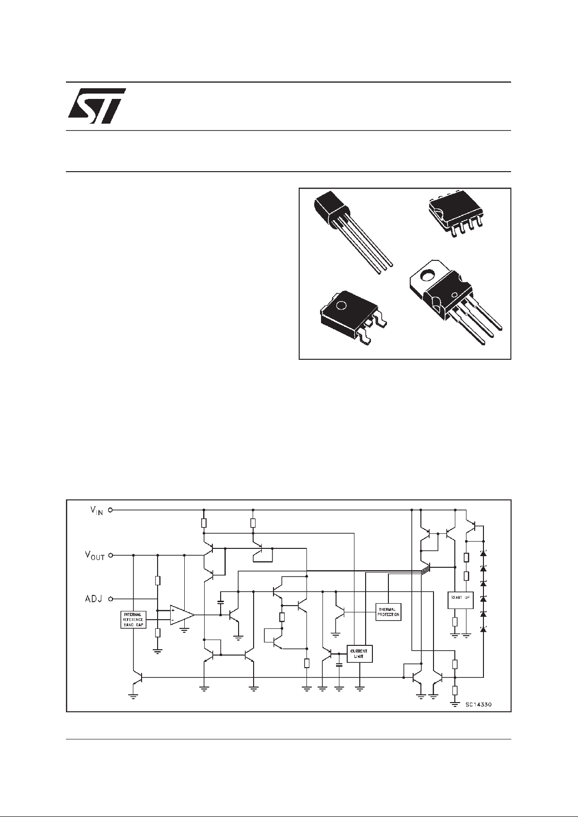
BLOCKDIAGRAM
■ VERYLOWDROPOUTVOLTAGE (0.15V
TYP.AT 10mA LOAD)
■ LOWQUIESCENTCURRENT (TYP2.5mA,
AT 100mA LOAD)
■
OUTPUT CURRENT UP TO 100mA
■ ADJUSTABLE(FROMV
OUT
=2.5VONLY
SO-8)ANDFIXED(3.3V& 5V) OUTPUT
VOLTAGEVERSION
■
INTERNALCURRENTAND THERMALLIMIT
■ LOADDUMP PROTECTIONUP TO60V
■ REVERSETRANSIENTPROTECTIONUPTO
-50V
■ TEMPERATURERANGE:-40TO 125
o
C
■ PACKAGEAVAILABLE:TO-92, DPAK,
TO-220,SO-8 (WITH INHIBITCONTROL)
DESCRIPTION
The LM2931 series are very low drop
regulators. The very low drop voltage and the
low quiescent current make them particular
suitable for low noise, low power applications
and in battery powered systems. In the 8 pin
configation (SO-8), fully compatible to the older
L78L00 family, a shut down Logic Control
function is available.
This means that when the device is used as a
local regulator is possible to put a part of the
board in stand-by decreasing the total power
consumption. Ideal for automotive application
the LM2931 is proteceted from reverse battery
installations or 2 battery jumps. During the
transient, suchs as a a load dump (60V) when
the input voltage can exceed the specified
maximum operating input voltage (26V), the
regulator will automatically shut down to protect
both internal circuit and the load.
TO-252 (DPAK) TO-220
SO-8
TO-92
1/16
Page 2
ABSOLUTE MAXIMUM RATINGS
Symbol Parameter Value Unit
V
IN
DC PositiveInputVoltage 40 V
V
IN
DC Reverse InputVoltage -15 V
V
IN
TransientInput Voltage(τ<100ms)
60 V
V
IN
TransientReverse InputVoltage (τ < 100ms)
-50 V
V
INH
InhibitInputVoltage 40 V
I
OUT
OutputCurrent Internally Limited mA
T
stg
Storage TemperatureRange -65 to 150
o
C
T
op
OperatingJunction Temperature Range -40 to 125
o
C
Absolute Maximum Ratings are those value beyond which damage to the device may occur. Functional operation under these condition is
not implied.
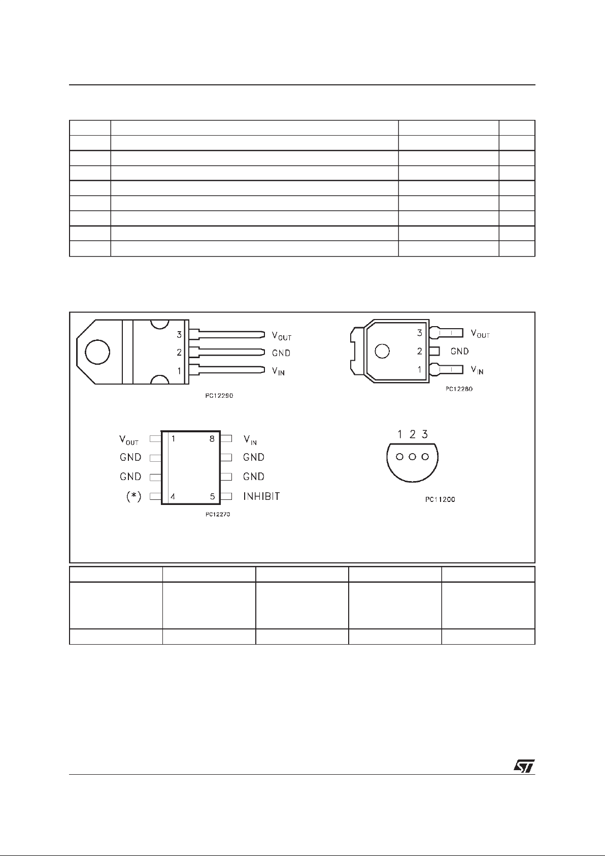
CONNECTION DIAGRAM AND ORDERINGNUMBERS
(top view)
TO-220 DPAK (*) TO-92 (*) SO-8 (*) Output Voltage
LM2931AV33
LM2931BV33
LM2931AV50
LM2931BV50
LM2931ADT33
LM2931BDT33
LM2931ADT50
LM2931BDT50
LM2931AZ33
LM2931BZ33
LM2931AZ50
LM2931BZ50
LM2931AD33
LM2931BD33
LM2931AD50
LM2931BD50
3.3V
3.3V
5V
5V
LM2931D 2.5V to 26V
(*) Available in Tape & Reel with the suffix”R” for fixedversion and ”-R” for adjustable version.
TO-220 DPAK
SO-8 TO-92
pin 1 = OUT
pin 2 = GND
pin 3 = IN
BOTTOM VIEW
(*)= N.C. for FIXED and ADJ for ADJUSTABLE
LM2931 SERIES
2/16
Page 3
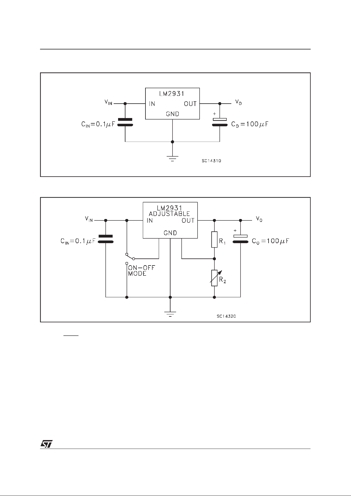
APPLICATION CIRCUIT FOR FIXED OUTPUT
(Figure1)
APPLICATION CIRCUIT FOR ADJUSTABLE OUTPUT(Figure 2)
R1suggestedValue = 27KΩ
V
O=VREF
x
R
1
+ R
2
R
1
LM2931 SERIES
3/16
Page 4
ELECTRICAL CHARACTERISTICS FOR LM2931A 3.3V
(referto the test circuits,
T
j
=25oC, VIN=14V, CIN= 0.1 µF, CO= 100 µF, IO=10mA, V
INH
= 0V unless otherwise specified)
Symbol Parameter Test Conditions Min. Typ. Max. Unit
V
I
Maximum OperatingInput
Voltage
IO=10mA Tj=-40to 125oC2637 V
V
O
OutputVoltage 3.175 3.3 3.425 V
V
O
OutputVoltage IO= 100mA VIN=6 to 26 V
T
j
= -40to 125oC
3.135 3. 3 3.465 V
∆V
O
LineRegulation VIN=9 to 16 V 2 10 mV
∆V
O
LineRegulation VIN=6 to 26 V 4 33 mV
∆V
O
LoadRegulation IO= 5 to100 mA 10 33 mV
V
d
Dropout Voltage (Note1, 2) IO= 10 mA 90 250 V
V
d
Dropout Voltage (Note1, 2) IO= 100mA 250 600 V
I
d
QuiescentCurrent ON Mode: I
OUT
= 100mA 2.5 30 mA
I
d
QuiescentCurrent
OFFMode: V
INH
=2.5V R
LOAD
=330Ω
0.3 1 mA
I
SC
ShortCircuitCurrent 100 300 mA
SVR Supply VoltageRejection
I
O
= 100mA VIN=14±2V
f = 120Hz T
j
= -40to 125oC
55 78 dB
V
IL
Control InputVoltage Tj= -40to 125oC21.2V
V
IH
Control InputVoltage Tj= -40to 125oC3.252V
I
INH
InhibitInput Current V
INH
=2.5V 22 50
µA
V
IN
TransientInput Voltage
R
LOAD
=330Ωτ<100ms
60 70 V
V
IN
Reverse PolarityInput
Voltage
V
O
± 0.3V R
LOAD
=330Ω
-15 -50 V
V
IN
Reverse PolarityInput
VoltageTransient
R
LOAD
=330Ωτ<100ms
-50 V
eN OutputNoise Voltage B = 10Hzto 100KHz 330
µ
V
RMS
Note 1: Reference Voltage is measured from V
OUT
to AJD pin.
Note 2: V
d
measured when the output voltage has dropped 100mV from the nominal value obtained at 14V.
LM2931 SERIES
4/16
Page 5
ELECTRICAL CHARACTERISTICS FOR LM2931B 3.3V
(referto the test circuits,
T
j
=25oC, VIN=14V, CIN= 0.1 µF, CO= 100 µF, IO=10mA, V
INH
= 0V unless otherwise specified)
Symbol Parameter Test Conditions Min. Typ. Max. Unit
V
I
Maximum OperatingInput
Voltage
IO=10mA Tj=-40to 125oC2637 V
V
O
OutputVoltage 3.135 3.3 3.465 V
V
O
OutputVoltage IO= 100mA VIN=6 to 26 V
T
j
= -40to 125oC
2.97 3.3 3.63 V
∆V
O
LineRegulation VIN=9 to 16 V 2 10 mV
∆V
O
LineRegulation VIN=6 to 26 V 4 33 mV
∆V
O
LoadRegulation IO= 5 to100 mA 10 33 mV
V
d
Dropout Voltage (Note1, 2) IO= 10 mA 90 200 V
V
d
Dropout Voltage (Note1, 2) IO= 100mA 250 600 V
I
d
QuiescentCurrent ON Mode: I
OUT
= 100mA 2.5 30 mA
I
d
QuiescentCurrent
OFFMode: V
INH
=2.5V R
LOAD
=330Ω
0.3 1 mA
I
SC
ShortCircuitCurrent 100 300 mA
SVR Supply VoltageRejection
I
O
= 100mA VIN=14±2V
f = 120Hz T
j
= -40to 125oC
55 78 dB
V
IL
Control InputVoltage Tj= -40to 125oC21.2V
V
IH
Control InputVoltage Tj= -40to 125oC3.252V
I
INH
InhibitInput Current V
INH
=2.5V 22 50
µA
V
IN
TransientInput Voltage
R
LOAD
=330Ωτ<100ms
60 70 V
V
IN
Reverse PolarityInput
Voltage
V
O
± 0.3V R
LOAD
=330Ω
-15 -50 V
V
IN
Reverse PolarityInput
VoltageTransient
R
LOAD
=330Ωτ<100ms
-50 V
eN OutputNoise Voltage B = 10Hzto 100KHz 330
µ
V
RMS
Note 1: Reference Voltage is measured from V
OUT
to AJD pin.
Note 2: V
d
measured when the output voltage has dropped 100mV from the nominal value obtained at 14V.
LM2931 SERIES
5/16
Page 6

ELECTRICAL CHARACTERISTICS FOR LM2931A 5V
(referto the test circuits,
T
j
=25oC, VIN=14V, CIN= 0.1 µF, CO= 100 µF, IO=10mA, V
INH
= 0V unless otherwise specified)
Symbol Parameter Test Conditions Min. Typ. Max. Unit
V
I
Maximum OperatingInput
Voltage
IO=10mA Tj=-40to 125oC2637 V
V
O
OutputVoltage 4.81 5 5.19 V
V
O
OutputVoltage IO= 100mA VIN=6 to 26 V
T
j
= -40to 125oC
4.75 5 5.25 V
∆V
O
LineRegulation VIN=9 to 16 V 2 10 mV
∆V
O
LineRegulation VIN=6 to 26 V 4 30 mV
∆V
O
LoadRegulation IO= 5 to100 mA 15 50 mV
V
d
Dropout Voltage (Note1, 2) IO= 10 mA 90 200 V
V
d
Dropout Voltage (Note1, 2) IO= 100mA 250 600 V
I
d
QuiescentCurrent ON Mode: I
OUT
= 100mA 2.5 30 mA
I
d
QuiescentCurrent
OFFMode: V
INH
=2.5V R
LOAD
=500Ω
0.3 1 mA
I
SC
ShortCircuitCurrent 100 300 mA
SVR Supply VoltageRejection
I
O
= 100mA VIN=14±2V
f = 120Hz T
j
= -40to 125oC
55 75 dB
V
IL
Control InputVoltage Tj= -40to 125oC21.2V
V
IH
Control InputVoltage Tj= -40to 125oC3.252V
I
INH
InhibitInput Current V
INH
=2.5V 22 50
µA
V
IN
TransientInput Voltage
R
LOAD
=500Ωτ<100ms
60 70 V
V
IN
Reverse PolarityInput
Voltage
V
O
± 0.3V R
LOAD
=500Ω
-15 -50 V
V
IN
Reverse PolarityInput
VoltageTransient
R
LOAD
=500Ωτ<100ms
-50 V
eN OutputNoise Voltage B = 10Hzto 100KHz 500
µ
V
RMS
Note 1: Reference Voltage is measured from V
OUT
to AJD pin.
Note 2: V
d
measured when the output voltage has dropped 100mV from the nominal value obtained at 14V.
LM2931 SERIES
6/16
Page 7

ELECTRICAL CHARACTERISTICS FOR LM2931B 5V
(referto the test circuits,
T
j
=25oC, VIN=14V, CIN= 0.1 µF, CO= 100 µF, IO=10mA, V
INH
= 0V unless otherwise specified)
Symbol Parameter Test Conditions Min. Typ. Max. Unit
V
I
Maximum OperatingInput
Voltage
IO=10mA Tj=-40to 125oC2637 V
V
O
OutputVoltage 4.75 5 5.25 V
V
O
OutputVoltage IO= 100mA VIN=6 to 26 V
T
j
= -40to 125oC
4.555.5V
∆V
O
LineRegulation VIN=9 to 16 V 2 10 mV
∆V
O
LineRegulation VIN=6 to 26 V 4 30 mV
∆V
O
LoadRegulation IO= 5 to100 mA 15 50 mV
V
d
Dropout Voltage (Note1, 2) IO= 10 mA 90 200 V
V
d
Dropout Voltage (Note1, 2) IO= 100mA 250 600 V
I
d
QuiescentCurrent ON Mode: I
OUT
= 100mA 2.5 30 mA
I
d
QuiescentCurrent
OFFMode: V
INH
=2.5V R
LOAD
=330Ω
0.3 1 mA
I
SC
ShortCircuitCurrent 100 300 mA
SVR Supply VoltageRejection
I
O
= 100mA VIN=14±2V
f = 120Hz T
j
= -40to 125oC
55 75 dB
V
IL
Control InputVoltage Tj= -40to 125oC21.2V
V
IH
Control InputVoltage Tj= -40to 125oC3.252V
I
INH
InhibitInput Current V
INH
=2.5V 22 50
µA
V
IN
TransientInput Voltage
R
LOAD
=500Ωτ<100ms
60 70 V
V
IN
Reverse PolarityInput
Voltage
V
O
± 0.3V R
LOAD
=500Ω
-15 -50 V
V
IN
Reverse PolarityInput
VoltageTransient
R
LOAD
=500Ωτ<100ms
-50 V
eN OutputNoise Voltage B = 10Hzto 100KHz 500
µ
V
RMS
Note 1: Reference Voltage is measured from V
OUT
to AJD pin.
Note 2: V
d
measured when the output voltage has dropped 100mV from the nominal value obtained at 14V.
LM2931 SERIES
7/16
Page 8

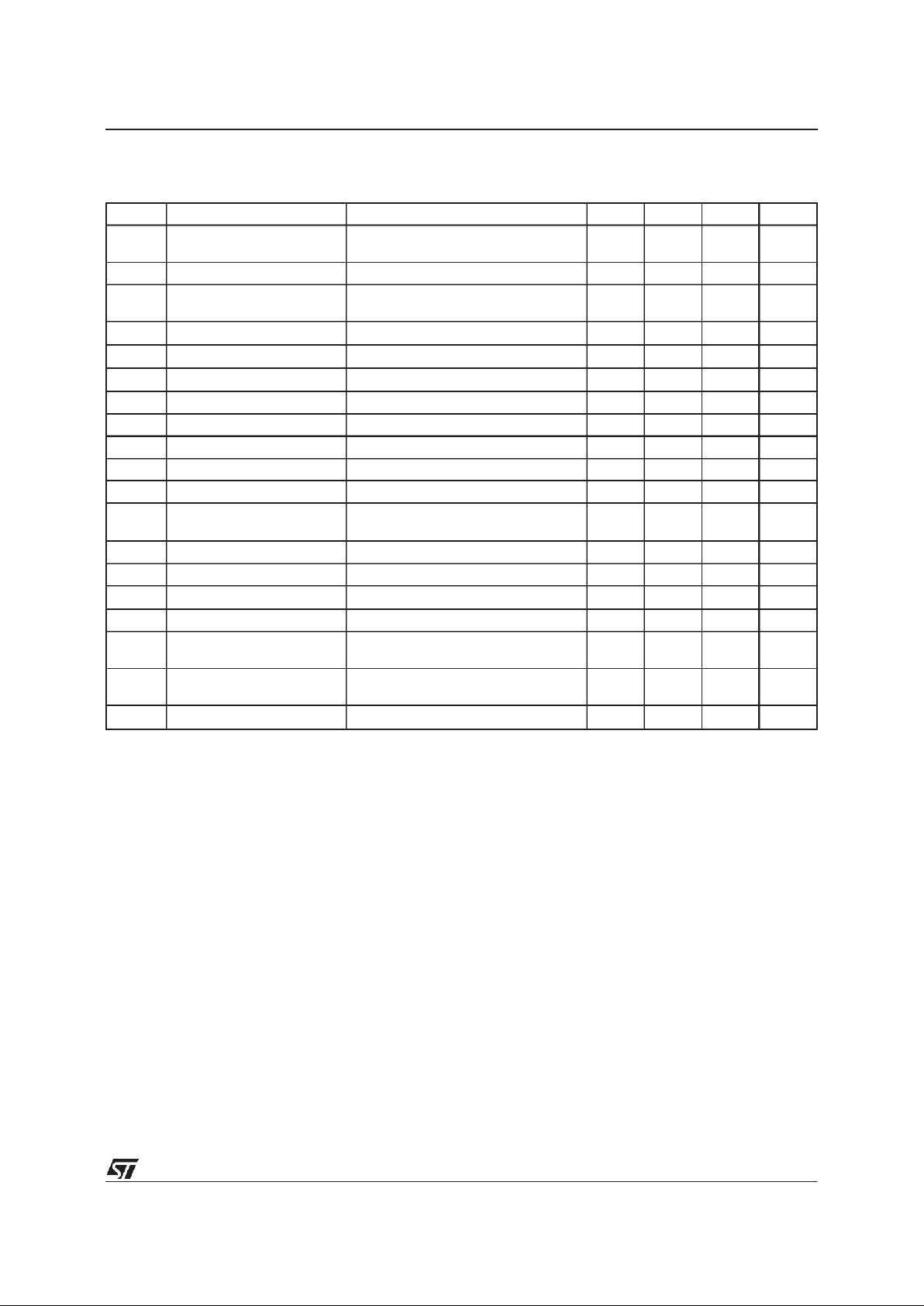
ELECTRICAL CHARACTERISTICS FOR LM2931ADJ
(referto the test circuitsfigure 2 with R
1
=27KΩ
and R
2
=40.5KΩ,Tj=25oC, VIN=14V, CIN= 0.1 µF, CO= 100 µF, IO= 10mA,V
INH
= 0V unless
otherwisespecified)
Symbol Parameter Test Conditions Min. Typ. Max. Unit
V
I
Maximum OperatingInput
Voltage
IO=10mA Tj=-40to 125oC2637 V
V
REF
Reference Voltage(Note 1) 1.14 1.2 1.26 V
V
REF
Reference Voltage(Note 1) IO= 100mA Tj=-40to 125oC 1.08 1.2 1.32 V
∆V
O
LineRegulation VIN=3.6 to 26 V 0.6 4.5 mV
∆V
O
LoadRegulation IO= 5 to100 mA 9 30 mV
V
d
Dropout Voltage (Note1, 2) IO= 10 mA 90 200 V
V
d
Dropout Voltage (Note1, 2) IO= 100mA 250 600 V
I
d
QuiescentCurrent ON Mode: I
OUT
= 100mA 2.5 30 mA
I
d
QuiescentCurrent
OFFMode: V
INH
=2.5V R
LOAD
=300Ω 0.3 1 mA
I
SC
ShortCircuitCurrent 100 300 mA
SVR Supply VoltageRejection
I
O
= 100mA VIN=14±2V
f = 120Hz T
j
= -40to 125oC
55 80 dB
V
IL
Control InputVoltage Tj= -40to 125oC21.2V
V
IH
Control InputVoltage Tj= -40to 125oC3.252V
I
INH
InhibitInput Current V
INH
=2.5V 22 50
µ
A
V
IN
TransientInput Voltage
R
LOAD
=300Ωτ<100ms
60 70 V
V
IN
Reverse PolarityInput
Voltage
V
O
±
0.3V R
LOAD
=300
Ω
-15 -50 V
V
IN
Reverse PolarityInput
VoltageTransient
R
LOAD
=300
Ωτ
<100ms
-50 V
eN OutputNoise Voltage B = 10Hzto 100KHz 330
µ
V
RMS
Note 1: Reference Voltage is measured from V
OUT
to AJD pin.
Note 2: V
d
measured when the output voltage has dropped 100mV from the nominal value obtained at 14V.
LM2931 SERIES
8/16
Page 9

TYPICALCHARACTERISTICS
(unlessotherwisespecifiedC
IN
=0.1µF,CO=100µF)
OutputVoltage vs Temperature OutputVoltage vs Temperature
RefereceVoltage vs Temperature
LoadRegulation vs Temperature
Line Regulationvs Temperature
Dropout Voltagevs Temperature
LM2931 SERIES
9/16
Page 10

DropoutVoltagevs Temperature
OutputVoltage vs Input Voltage
QuiescentCurrent vs Temperature
Dropout Voltagevs OutputCurrent
Short Circuit Currentvs Drop Voltage
QuiescentCurrent vs InputVoltage
TYPICALCHARACTERISTICS
(Continued)
LM2931 SERIES
10/16
Page 11

QuiescentCurrent vs OutputCurrent
SupplyVoltage Rejectionvs Frequency
Line Transient
SupplyVoltage Rejectionvs Temperature
SupplyVoltage Rejectionvs Output Current
LoadTransient
TYPICALCHARACTERISTICS
(Continued)
LM2931 SERIES
11/16
Page 12

DIM.
mm inch
MIN. TYP. MAX. MIN. TYP. MAX.
A 4.40 4.60 0.173 0.181
C 1.23 1.32 0.048 0.051
D 2.40 2.72 0.094 0.107
D1 1.27 0.050
E 0.49 0.70 0.019 0.027
F 0.61 0.88 0.024 0.034
F1 1.14 1.70 0.044 0.067
F2 1.14 1.70 0.044 0.067
G 4.95 5.15 0.194 0.203
G1 2.4 2.7 0.094 0.106
H2 10.0 10.40 0.393 0.409
L2 16.4 0.645
L4 13.0 14.0 0.511 0.551
L5 2.65 2.95 0.104 0.116
L6 15.25 15.75 0.600 0.620
L7 6.2 6.6 0.244 0.260
L9 3.5 3.93 0.137 0.154
DIA. 3.75 3.85 0.147 0.151
L6
A
C
D
E
D1
F
G
L7
L2
Dia.
F1
L5
L4
H2
L9
F2
G1
TO-220 MECHANICAL DATA
P011C
LM2931 SERIES
12/16
Page 13

DIM.
mm inch
MIN. TYP. MAX. MIN. TYP. MAX.
A 2.2 2.4 0.086 0.094
A1 0.9 1.1 0.035 0.043
A2 0.03 0.23 0.001 0.009
B 0.64 0.9 0.025 0.035
B2 5.2 5.4 0.204 0.212
C 0.45 0.6 0.017 0.023
C2 0.48 0.6 0.019 0.023
D 6 6.2 0.236 0.244
E 6.4 6.6 0.252 0.260
G 4.4 4.6 0.173 0.181
H 9.35 10.1 0.368 0.397
L2 0.8 0.031
L4 0.6 1 0.023 0.039
==
D
L2
L4
13
==
B
E
==
B2
G
2
A
C2
C
H
A1
DETAIL”A”
A2
DETAIL”A”
TO-252 (DPAK) MECHANICAL DATA
0068772-B
LM2931 SERIES
13/16
Page 14

DIM.
mm inch
MIN. TYP. MAX. MIN. TYP. MAX.
A 1.75 0.068
a1 0.1 0.25 0.003 0.009
a2 1.65 0.064
a3 0.65 0.85 0.025 0.033
b 0.35 0.48 0.013 0.018
b1 0.19 0.25 0.007 0.010
C 0.25 0.5 0.010 0.019
c1 45 (typ.)
D 4.8 5.0 0.188 0.196
E 5.8 6.2 0.228 0.244
e 1.27 0.050
e3 3.81 0.150
F 3.8 4.0 0.14 0.157
L 0.4 1.27 0.015 0.050
M 0.6 0.023
S 8 (max.)
0016023
SO-8 MECHANICALDATA
LM2931 SERIES
14/16
Page 15

DIM.
mm inch
MIN. TYP. MAX. MIN. TYP. MAX.
A 4.58 5.33 0.180 0.210
B 4.45 5.2 0.175 0.204
C 3.2 4.2 0.126 0.165
D 12.7 0.500
E 1.27 0.050
F 0.4 0.51 0.016 0.020
G 0.35 0.14
TO-92 MECHANICAL DATA
LM2931 SERIES
15/16
Page 16

Information furnished isbelieved to be accurate and reliable. However,STMicroelectronics assumes no responsibility for the consequences
of use of such information nor for any infringement of patents or other rights of third parties which may result from its use. No license is
granted by implication or otherwise under any patent or patent rights of STMicroelectronics. Specification mentioned in this publication are
subject tochange without notice. Thispublication supersedes and replaces all information previously supplied. STMicroelectronics products
are not authorized for use as critical components in life support devices or systems withoutexpress written approval of STMicroelectronics.
The ST logo isa registeredtrademark of STMicroelectronics
1999 STMicroelectronics – Printed in Italy– All Rights Reserved
STMicroelectronics GROUP OF COMPANIES
Australia - Brazil- China - Finland - France - Germany - HongKong - India- Italy - Japan- Malaysia - Malta - Morocco
Singapore - Spain- Sweden- Switzerland - United Kingdom - U.S.A.
http://www.st.com
.
LM2931 SERIES
16/16
 Loading...